NPC CF8223A Datasheet

µ m × 90 µ
SM8223A
NIPPON PRECISION CIRCUITS INC.
FSK Decoder and DTMF Receiver IC
OVERVIEW
The SM8223A is a FSK (Frequency shift keying) decoder and DTMF (Dual tone multi-frequency) receiver IC.
It is fabricated using a CMOS process and features a power-down function for low power dissipation operation. The FSK decoder and DTMF receiver have the same performance characteristics as dedicated ICs that
perform the same functions, with the added benefit of an FSK decoder/DTMF receiver auto-select function
using the telephone tip/ring input signal. It also features a ring (call signal) signal detection circuit, making for
easy construction of low power dissipation, high-performance analog telephone-related applications.
FEATURES
■
Both FSK signal caller-ID information services
PINOUT
(Top view)
and DTMF signal caller-ID information services
supported
■
FSK decoder/DTMF receiver auto-select function
■
Ring (call signal) signal detection circuit built-in
■
Serial I/O
■
Input gain adjustment circuit built-in
■
Power-down mode
■
Single supply operation: 3.0V ± 10%
■
3.579545MHz external crystal oscillator frequency
■
Molybdenum-gate CMOS process
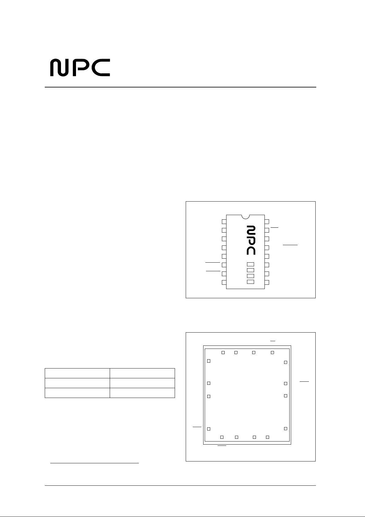
TIP
RING
GS
AGND
RDIN
RDRC
RDET
PDWN
1
SM8223AP
8
16
9
VDD
DV
DOUT
FSK/DTMF
IC
OSCIN
OSCOUT
GND
APPLICATIONS
1
■
Telephones, fax machines and modems that support caller-ID information services
■
Adapters for caller-ID information service functions
■
Telephones, fax machines and modems that support remote operation functions
ORDERING INFORMATION
De vice Pack ag e
SM8223A 16-pin DIP
CF8223A Chip
PINOUT
(Unit: µ m)
GS
AGND
RDIN
RDRC
(0, 0)
RING TIP VDD DV
PDWN GND OSCOUT
RDET
Pad size : 9 0
m
1. Auto-select function operates if the FSK signal conforms to the Bellcore GR-30-CORE standard.
(2810, 3160)
DOUT
FSK/DTMF
IC
OSCIN
NIPPON PRECISION CIRCUITS—1

PACKAGE DIMENSIONS
(Unit: mm)
19.05
SM8223A
6.35
7.49 to 8.13
8.13 to 9.40
0.25
3.18 3.30
BLOCK DIAGRAM
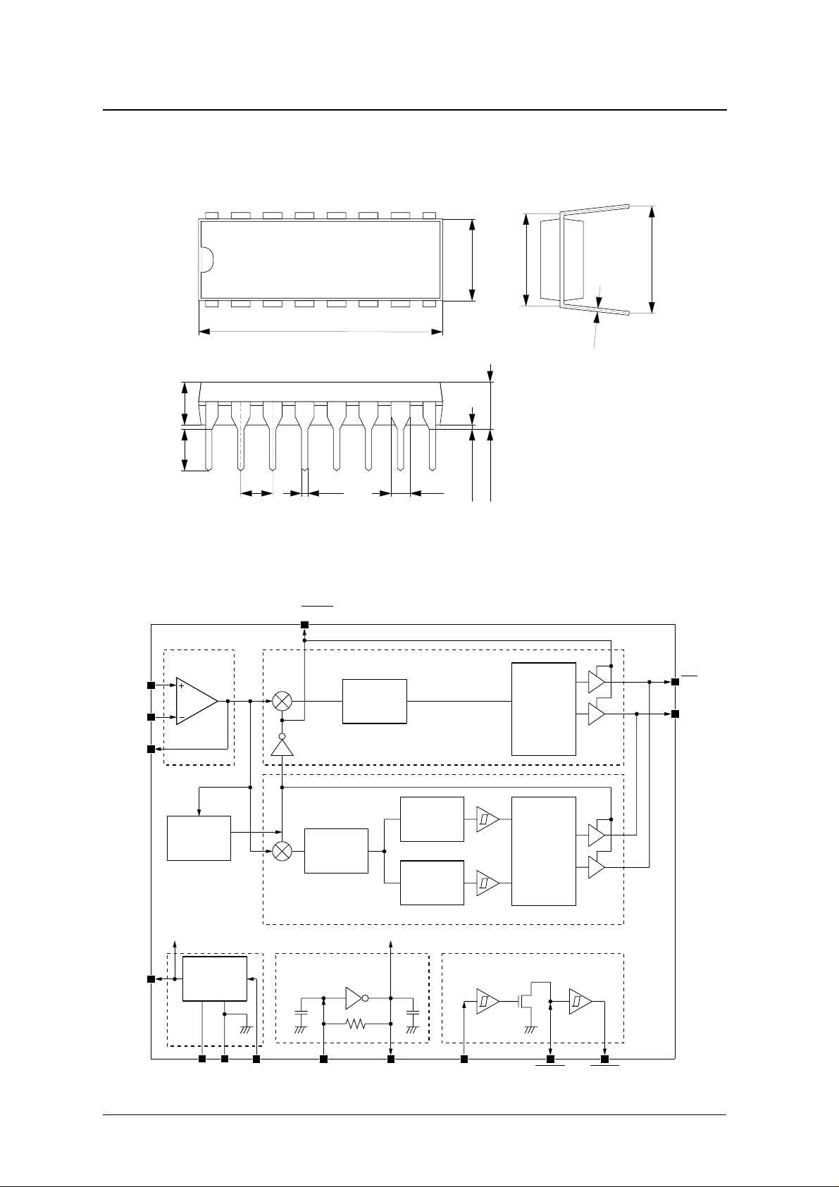
Differential
Amplifier
TIP
RING
GS
FSK/DTMF
Discriminator
Logic
2.54
2.54 0.46 1.52
FSK/DTMF
FSK Decoder
Band Pass
Filter
High Group
Filter
Dial Tone
Filter
Low Group
Filter
3.68 to 4.32
0.38 to 1.02
FSK
Decoder
Logic
DTMF
Decoder
Logic
DV
DOUT
AGND
Bias
Circuit
GNDVDD PDWN
DTMF Receiver
OSC Ring Detect
OSCIN OSCOUT RDIN
RDRC RDET
NIPPON PRECISION CIRCUITS—2

µ
PIN DESCRIPTION
SM8223A
Number Name I/O Function
1 TIP I Tip input. Connected to the telephone line through a protection circuit 1046 2934
2 RING I Ring input. Connected to the telephone line through a protection circuit 63 8 2934
3GSO
4 AG N D O Analog ground output. Inter nal reference voltage (V
5 RDIN I
6 RDRC
7 RDET
8PDWNI
9 G ND – Ground. Connected to the system ground potential. 1634 226
10 OSCOUT O
11 OSCIN I
12 I C I Test input. Tied LOW for normal operation. 2634 1550
13 FSK/DTMF
14 DOUT O
15 D
16 V D D – Supply 1612 2934
V O Data trigger output. Data is output on DOUT when this pin goes LOW. 2211 2934
Input-stage amplifier gain-select output. Used to adjust the gain of the inputstage amplifier.
/2) output level 17 6 1954
DD
Ring detector input. Used for line reversal and ring signal detection.
Connected for ring detection of attenuated ring signals.
Ring detector RC terminal. Connected to an RC network which sets the ring
I/O
detector delay time.
Ring detector output. RDRC
O
output when ring signal is detected.
Pow er-down control input. LOW-level for normal operation. HIGH-level for
pow er-down state. In the pow er-down state, pins AGND, OSCOUT, DOUT,
and DV are HIGH.
Cr ystal oscillator output. The cr ystal oscillator element is connected between
this pin and OSCIN.
Crystal oscillator input. The crystal oscillator element is connected between
this pin and OSCOUT.
FSK/DTMF discriminator output. HIGH-level output when receiving FSK
O
signal, and LOW -level output when receiving DTMF signal.
Demodulator output. Demodulated FSK or DTMF signal output. HIGH-level
output in pow er-down state.
-input Schmitt-trigger buffer output. L OW -level
Pad dimensions (
XY
176 2665
176 1534
176 492
596 226
1063 226
2053 226
2634 506
2634 1942
2634 2623
m)
NIPPON PRECISION CIRCUITS—3

−
−
−
° C
∆
−
−
° C
SM8223A
SPECIFICATIONS
Absolute Maximum Ratings
GND = 0V
Parameter Symbol Rating Unit
Supply voltage range V
Input voltage range V
DC input current I
Storage temperature range T
Recommended Operating Conditions
GND = 0V
−
−
DD
IN
IN
stg
0.5 to 5.0 V
0.3 to V
+ 0.3 V
DD
±10 m A
40 to 125
Parameter Symbol Condition
Supply voltage V
Clock frequency f
Clock frequency accuracy
Operating temperature T
DC Electrical Characteristics
V
= 3.0V ± 0.3V, GND = 0V, f
DD
Parameter Symbol Condition
Supply current consumption I
Power-down state current I
PD WN, RDIN, RDRC LOW -level
input voltage
PD WN, RDIN, RDRC
HIGH-level
input voltage
OSCIN LOW-level input voltage V
OSCIN HIGH-level input voltage V
DOUT, DV, RDET, FSK/DTMF LOW -
level output current
V, RDET, FSK/DTMF HIGH-
DOUT, D
level output current
P DWN, RDIN input leakage current I
RDRC output leakage current I
CLK
DPD
V
V
I
DD
CLK
f
C
a
= 3.579545MHz, T
P DW N = 0V, RDIN = 0V,
DD
IL1
IH1
IL2
IH2
I
OL
OH
IN
OFF
RDRC = 0V, all other inputs
open
PDWN = V
RDRC = 0V, all other inputs
open
When external clock input – – 0.3V
When external clock input 0.7V
Rating
min typ max
2.7 – 3.3 V
– 3.579545 – MH z
0.1 – +0.1 %
20 – 85
= − 20 to 85 ° C unless otherwise noted.
a
Rating
min typ max
– – 4.5 mA
, RDIN = 0V,
DD
––15µA
– – 0.3V
0.7V
DD
DD
––V
––V
2––mA
––
1– 1µA
––1µA
Unit
Unit
DD
DD
0.8 m A
V
V
NIPPON PRECISION CIRCUITS—4

AC Electrical Characteristics
FSK decoder
V
= 3.0V ± 0.3V, GND = 0V, f
DD
CLK
SM8223A
= 3.579545MHz, T
− 40 −
−
−
Ω
= − 20 to 85 ° C unless otherwise noted.
a
Parameter Symbol Condition
Detection sensitivity Typical application circuit
Ma rk signal and SPACE
Noise reduction ratio
signal are same level.
Noise: Random noise from
200Hz to 3400Hz.
min typ max
20 – – d B
Rating
Unit
37.5 0 d B m
DTMF receiver
V
= 3.0V ± 0.3V, GND = 0V, f
DD
Parameter Symbol Condition
Detection frequency deviation
Non-detection frequency deviation ±3.5 – – %
Detection sensitivity
Non-detection sensitivity ––
Signal level error
High-frequency rejection ratio – 1 8 – d B
Noise rejection ratio –12–dB
Dial tone rejection ratio –20–dB
1. Input signal is up to V
DD
level.
= 3.579545MHz, T
CLK
Typical application circuit
Typical application circuit
= − 20 to 85 ° C unless otherwise noted.
a
Rating
min typ max
±1.5% ± 2 – – Hz
32.0 – 0.0 dB m
50.0 dB m
––6dB
1
Unit
Input-stage amplifier Characteristics
V
= 3.0V ± 0.3V, GND = 0V, f
DD
Parameter Symbol Condition
Input leakage current I
Input resistance R
DC open-loop voltage gain A
Unity gain frequency f
Load capacitance C
Load resistance R
= 3.579545MHz, T
CLK
IN
IN
VOL
C
L
L
= − 20 to 85 ° C unless otherwise noted.
a
Rating
min typ max
––1µA
–1–M
30 – – d B
80 – – kHz
– – 100 pF
50 – – k Ω
Unit
NIPPON PRECISION CIRCUITS—5
 Loading...