−
CF5746 Series
NIPPON PRECISION CIRCUITS INC.
OVERVIEW
The CF5746 Series devices are analog clock ICs that
derive their timing from a 32 kHz oscillator element.
They feature alarm outputs, snooze function and
alarm auto-stop function. They can be configured to
match a wide variety of clock specifications, alarm
functions and motor outputs.
FEATURES
■
32.768 kHz oscillator circuit
•R
and R
f
built-in
d
• Oscillator capacitance built-in
-C
= 30 pF (typ, excluding CF5746ADC)
D
-C
= 20 pF (typ, CF5746ADC)
D
SERIES CONFIGURATION
CMOS Analog Clock IC
■
Alarm outputs
• Compatible with electronic sound alarms and
motor bells
• 4-step increasing volume alarm output
(CF5746AAB, ADC, AEA, AFA (AO1), AGA
(AO1))
■
Snooze function
• Temporarily stops alarm output and then restarts after a fixed time
■
Debouce circuit (AI/SNZ pin)
■
Test functions
• Shortening snooze time and auto-stop time
• Increasing motor speed (excluding
CF5746BCA)
Power-ON clear function
■
1.5 V supply voltage
■
Chip form
■
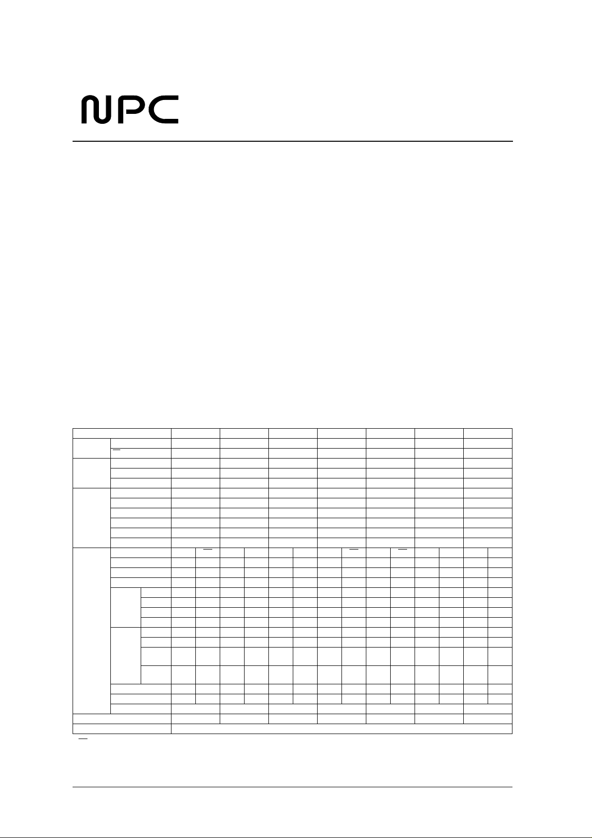
CF5746AAB CF5746ABA CF5746BCA CF5746ADC CF5746AEA CF5746AFA CF5746AGA
XT pin C
Built-in
capacitance
Motor output
AI/SNZ input
Alarm output
Pad layout AABAAAA
Other Power-ON clear, oscillator R
1. A
O has the opposite polarity to AO only when output (same phase when non-active).
2. AS = auto-stop
(pF) None None None None None None None
G
pin C
XT
(pF) 30 30 30 20 30 30 30
G
Active level HIGH HIGH – HIGH HIGH HIGH HIGH
Needle period t
Pulsewidth t
Alarm active level LOW LOW LOW HIGH LOW LOW LOW
Pin type 512 Hz 512 Hz 512 Hz 512 Hz 512 Hz Pull-up Pull-up
SNZ interface Yes Yes Yes No Yes Yes Yes
SNZ time t
Bounce delay (ms) 31.25 31.25 31.25 31.25 31.25 31.25 31.25
SNZ release No No No No No Yes (2 s) Ye s (2 s)
Pins AO A
Active level HIGH LOW
Frequency f
Modulation f
Duty (%)
Step time
(s)
min (mA)
I
OH
I
min (mA) 0.8 0.8 0.8 0.8 0.8 0.8 0.002 0.002 0.8 0.8 0.002 0.8 0.002 0.8
OL
Auto-stop t
CY
(s) 1 1 0.125 1111
PW
(ms) 23.4375 31.25 50% duty 46.875 31.25 46.875 31.25
(s) 256 256 256 256 256 256 256
SNZ
O AO1 AO2 AO1 AO2 AO AO AO AO AO1 AO2 AO1 AO2
1
PW
(Hz) 4096 4096 DC DC D C DC 2048 2048 2048 2048 2048 DC 2048 DC
(Hz) 8+1 8+1 ––––8+18+18+18+18+1–8+1–
CY
Step 1 12.5 12.5 ––––6.26 6.26 6.26 6.26 12.5 – 6.26 –
Step 2 25 25 ––––12.5 12.5 12.5 12.5 25 – 12.5 –
Step 3 50 50 ––––2525505050–50–
Step 4 ––––––5050––––––
Step 1 0 to 7 0 to 7 ––––0 to 30 to 30 to 70 to 70 to 7–0 to 7–
Step 2 7 to 15 7 to 15 ––––3 to 73 to 77 to 157 to 157 to 15–7 to 15–
Step 3
Step 4 ––––––
STOP
15 to
2
AS
0.8 − 0.8 − 0.8 − 0.8 − 0.8 − 0.8 − 0.8 − 0.8 − 0.8 − 0.8 − 0.8 − 0.8 − 0.8 − 0.8
(s) 128 128 128 128 128 128 128
HIGH HIGH HIGH HIGH HIGH LOW
15 to
––––7 to 317 to 31
AS
31 to AS31 to
1
HIGH LOW
15 to AS15 to AS15 to
––––––
AS
and R
d
f
built-in
1
HIGH HIGH HIGH HIGH
–
AS
15 to
AS
–
NIPPON PRECISION CIRCUITS—1

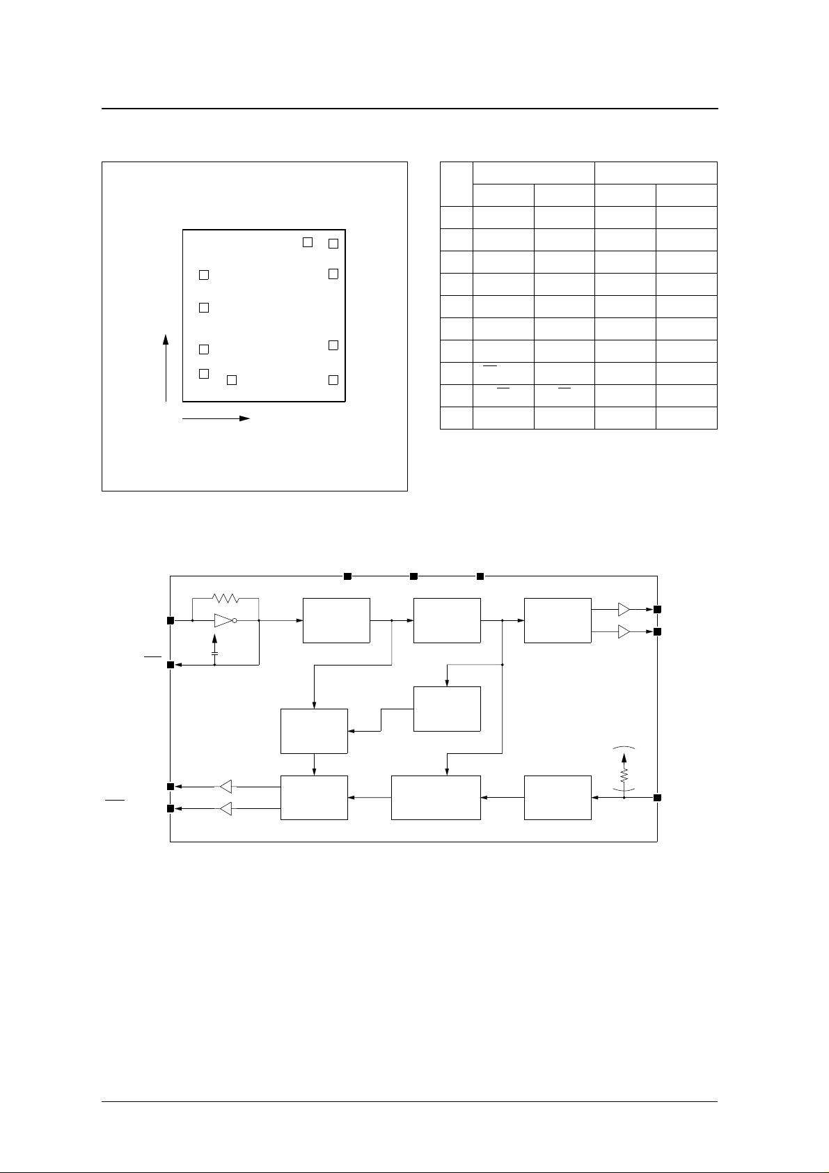
PAD DIMENSIONS
CF5746 Series
1
2
3
Y
4
(0, 0)
5
X
BLOCK DIAGRAM
10
9
8
7
6
TEST VSS
VDD
No.
1 VDD VSS 166 1210
2 VS S VDD 166 882
3 OUT1 AI/SNZ 166 474
4 AI/SNZ AO1 166 228
5 TEST AO2 444 169
6 OUT2 OUT1 1444 169
7 AO (AO1) OUT2 1444 513
8A
9XT XT 1444 1516
10 XT XT 1192 1531
Chip size: 1.61 × 1.70 mm
Chip thickness: 400 ± 30 µm
Pad size: 100 × 100 µm
Chip surface is at V
Layout Dimensions (µm)
A (ex. BCA) B (BCA) X Y
O (AO2) TEST 1444 1219
potential.
DD
XT
XT
AO(AO1)
AO(AO2)
CD
4- Stage
Divider
AO Duty
Control
Alarm
Out
11- Stage
Divider
4- Stage
Divider
Snooze
Counter
Output
Control
Input
Control
OUT1
OUT2
AI/SNZ
NIPPON PRECISION CIRCUITS—2

PIN DESCRIPTION
Name Description
VDD Positive supply voltage pin
VSS Ground pin
XT Oscillator input pin
XT
OUT1 Motor output pin 1
OUT2 Motor output pin 2
AI/SNZ Alarm/snooze input pin
AO (AO1) Alarm output pin
AO (AO2) Alarm output pin
TEST Test pin
Oscillator output pin
−
−
−
°
−
° C
−
−
−
−
− 1 − 3 −
∆
CF5746 Series
SPECIFICATIONS
Absolute Maximum Ratings
Parameter Symbol Condition Rating Unit
Supply voltage range V
Input voltage range V
Operating temperature range T
Storage temperature range T
Electrical Characteristics
T
= 25 ° C, V
a
Operating voltage V
Current consumption
Motor output current I
Alarm HIGH-level output current I
Alarm LOW-level output current
Alarm LOW-level output current
AI/SNZ HIGH-level input voltage V
AI/SNZ LOW-level input voltage V
AI/SNZ HIGH-level output current I
AI/SNZ LOW-level output current I
Oscillator frequency stability
VDD-to-XT pin built-in
capacitance
VDD-to-XT
capacitance
= 1.5 V, V
DD
Parameter Symbol Condition
1
2
3
pin built-in
= 0 V, f
SS
DD
DD
I
DD
MOT
OH
I
OL
IH
IL
OH
OL
f/f V
C
G
C
D
V
SS
IN
opr
stg
= 32.768 kHz unless otherwise noted
0
0.3 to 5.0 V
V
to V
SS
DD
30 to 70
40 to 125
Rating
min typ max
1.2 – 2.0 V
No load
– 1.0 2.0 µA
V
DD
V
DD
V
DD
= 1.2 V, R
= 1.2 V , V
= 1.2 V , V
= 200 Ω
L
= 0.7 V
OH
= 0.5 V 0.8 1.5 – mA
OL
±3.8 – – mA
0.8
1.5 – mA
21530µA
V
0.2 – V
DD
V
SS
V
= V
1.5 V
+ 1.5 V
Excluding
CF5746AFA,
AGA
1310µA
OH
DD
= V
V
OL
DD
= 1.2 to 2.0 V – 0.5 1 ppm/0.1 V
DD
–V
DD
+ 0.2 V
SS
10 µA
– None – pF
Excluding CF5746ADC – 30 – pF
CF5746ADC – 20 – pF
V
C
Unit
V
1. All pins except the supply and crystal oscillator pins are open.
2. CF5746AAB, ABA, BCA, AEA, AFA (AO2), AGA (AO2)
3. CF5746ADC, AFA (AO1), AGA (AO2)
NIPPON PRECISION CIRCUITS—3
 Loading...