− 8 + 1 − 8 +
CF5741 series
NIPPON PRECISION CIRCUITS INC.
OVERVIEW
The CF5741 series are analog clock driver ICs
using 32.768kHz reference frequency of crystal
oscillator. Some versions in accordance with the
combinations of each motor drive and alarm output
characteristics can provide a wide range of applications for various clock specifications.
FEATURES
■
Operating voltage 1.2 to 2.0V
■
Low current 1.2 µ A (typ) / 1.5V
■
Built-in oscillator circuits (32.768 kHz)
■
Built-in crystal oscillator capacitors (C
■
Motor output
Various motor output
■
Alarm output
Various alarm output
■
Reset function
■
Input debounce function (AI, RST/TC)
■
Chip form (CF5741 ×× )
, C
)
G
D
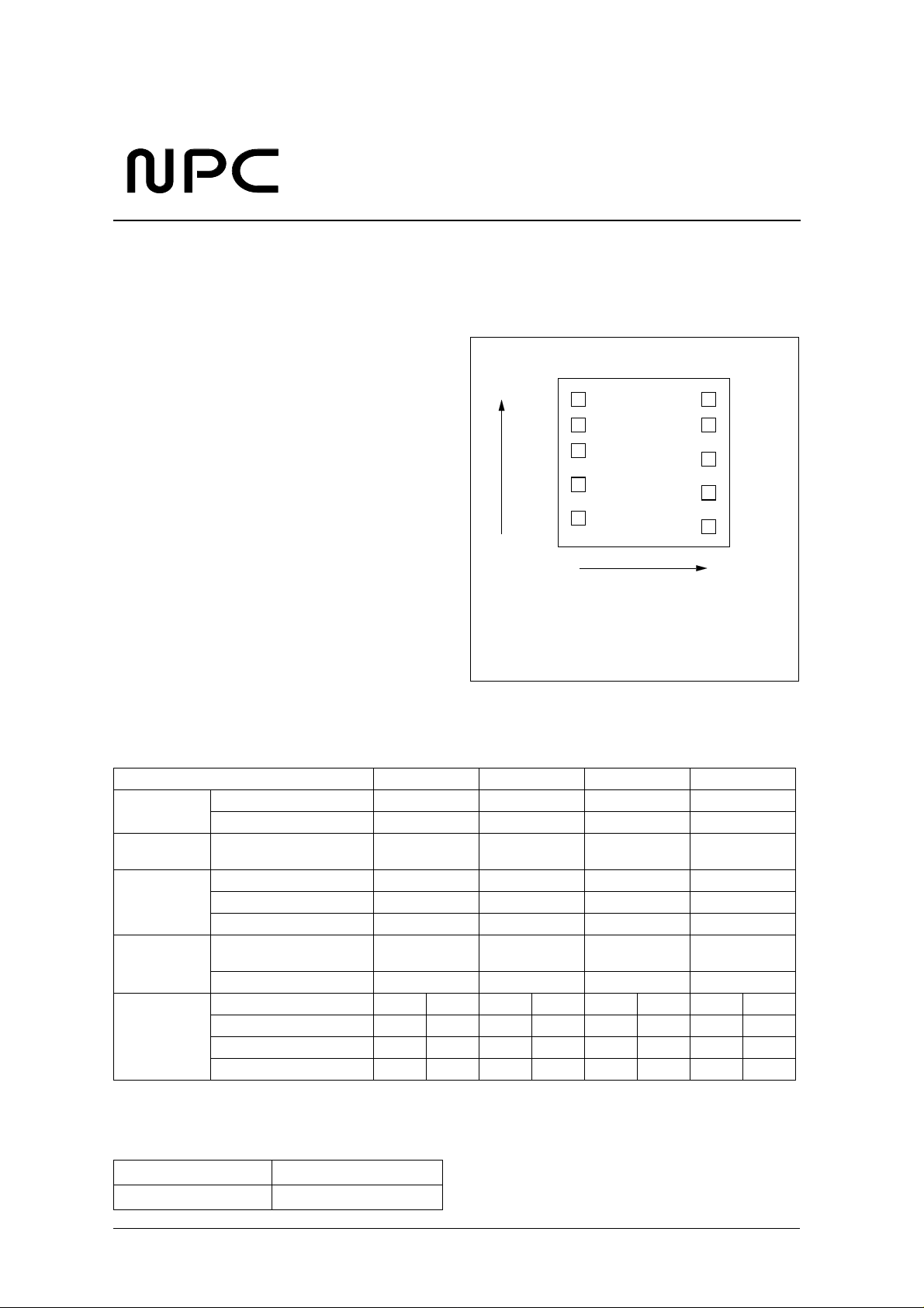
PINOUT
(T op V iew)
VSS
AO1
AO2/F
Y
XTN
Analog Clock CMOS IC
SA5741
1
2
3
4
XT
5
(0,0)
Chip size : 1.22 × 1.20 mm
Chip thickness : 400 ± 30 µ m
Pad size : 100 × 100 µ m
Reverse side : V
DD
10
9
8
7
6
X
level
OUT2
OUT1
AI
RST/TC
VDD
SERIES LINEUP
Built-in capacitor
Reset input Active level
Motor output
Alarm input
Alarm output
1. AO is complete reverse phase of AO. (even output is inactive.)
XT terminal C
XTN terminal C
Active level High High High High
Hand drive cycle t
Pulse width t
Active level
Test function (1/2V
Terminal AO1 AO2/F AO1 AO2/F AO1 AO2/F
Active level High High High High High Low High Low
Fundamental frequency f
Modulation frequency f
(pF) 0 25 0 27
G
(pF) 25 25 25 25
D
(sec) 1111
CY
(msec) 31.25 31.25 46.875 46.875
PW
) Yes Yes Yes Yes
DD
(Hz) 2048 32 2048 32 2048 2048 2048 2048
PW
(Hz) 8 + 1
CY
ORDERING INFORMATION
Device Package
CF5741 ××
Chip form
CF5741AA CF5741AB CF5741BA CF5741BB
Low
(Pull-up resistor)
Low
(Pull-up resistor)
Low
(Pull-up resistor)
Low
(Pull-up resistor)
Low
(Pull-up resistor)
Low
(Pull-up resistor)
1
18 + 18 + 18 + 1
Low
(Pull-up resistor)
Low
(Pull-up resistor)
AO1 AO2/F
1
NIPPON PRECISION CIRCUITS—1

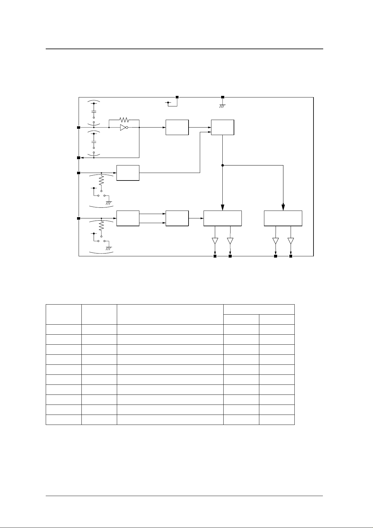
BLOCK DIAGRAM
CF5741 series
XT
XTN
RST/TC
AI
CG
CD
Reset
Input
Alarm
Input
Alarm
Test
VDD
4 Stage
Divider
AO
Test
VSS
13 Stage
Divider
Alarm Output
Control
AO1 AO2/F OUT1 OUT2
Motor Output
Control
PIN DESCRIPTION
Number Name Description
1 VSS Ground 147 1048
2 AO1 Alarm signal output1 147 867
3 AO2 / F Alarm signal output2/Frequency output 147 685
4 XTN Crystal oscillator connection 146 446
5 XT Crystal oscillator connection 146 206
6 VDD Power supply pin 1072 147
7 RST / TC Reset/Test clock input 1073 386
8 AI Alarm input 1073 626
9 OUT1 Motor drive output 1 1072 867
10 OUT2 Motor drive output 2 1072 1048
Dimensions ( µ m)
XY
NIPPON PRECISION CIRCUITS—2

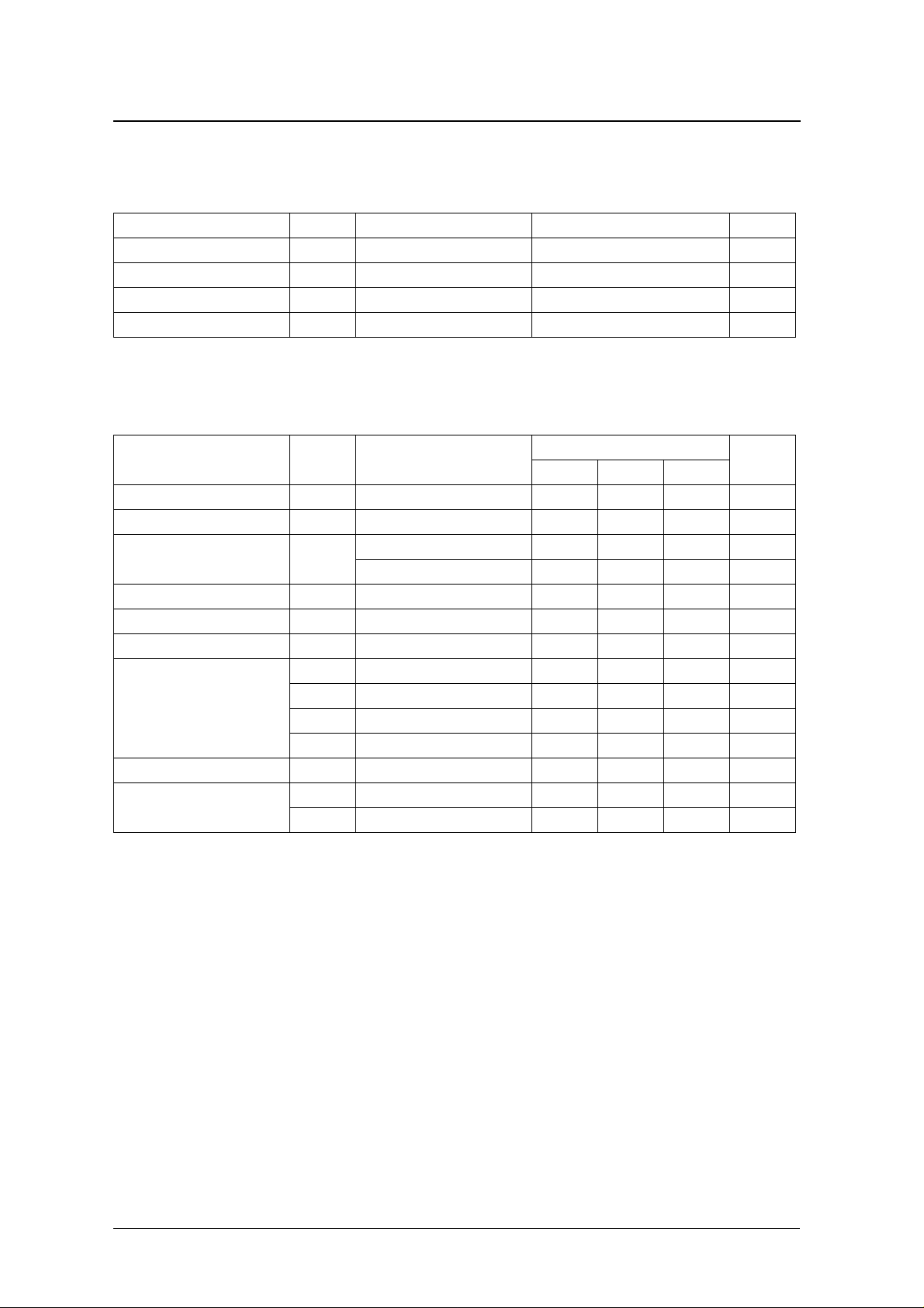
SPECIFICATIONS
Absolute Maximum Ratings
Parameter Symbol Condition Rating Unit
Supply voltage V
Input voltage V
Operating temperature T
Storage temperature T
Electrical Characteristics
DD
IN
OPR
STG
=
=
≤
−
−
≤
≤
−
°
−
° C
µ
=
=
=
=
=
∆
=
=
µ
=
µ
=
µ
=
µ
=
=
CF5741 series
V
SS
0.3 to 5.0 V
V
V
SS
V
IN
DD
30 to 80
65 to 150
V
C
Ta = 25 ° C, V
DD
1.5V, V
0V, X ′ tal (fo = 32.768kHz, C
SS
Parameter Symbol Condition
Supply voltage V
Current consumption I
Oscillator start-up time t
Motor output current I
Input resistance
2
(AI, RST/TC)
Oscillator stability
Alarm output current
(AO1, AO2/F)
Frequency output voltage V
Internal capacitance
1. R
is resistor of motor coil, that connect OUT1 between OUT2.
L
2. R
V
IN
DD
3. C
is internal capacitor between VDD and XT. C
G
3
/I
. I
is current that flow into VSS from AI, RST/TC, when AI, RST/TC short VSS. (AI,RST/TC build-in pull-up resistor.)
IS
IS
DD
DD
STA
MOT
R
IN
f/f V
I
OL1
I
OL2
I
OH1
I
OH2
F
C
G
C
D
D
35k Ω ), unless otherwise noted.
I
Rating
min typ max
1.2 1.5 2.0 V
OUT1, OUT2 = Open 1.2 4.0
V
1.2V 5.0 sec
DD
V
1.5V 2.0 sec
DD
V
1.2V, R
DD
L
200 Ω
1
4.0 mA
200 1200 k Ω
1.2V to 2.0V 0.5 1.0 ppm / 0.1V
DD
V
0.75V 900
OL
V
0.75V 10
OL
V
0.75V 900
OH
V
0.75V 10
OH
V
DD
1.2V, C
50pF 0.4 V
L
is internal capacitor between VDD and XTN.
Unit
A
A
A
A
A
pF
pF
NIPPON PRECISION CIRCUITS—3
 Loading...