NPC CF5732KA, CF5732JA, CF5732HA, CF5732GA, CF5732FA Datasheet
...
NIPPON PRECISION CIRCUITS INC.
NIPPON PRECISION CIRCUITS-1
OVERVIEW
CF5732 Series
Analog clock CMOS IC
The CF5732 series are analog clock driver ICs using
32kHz reference frequency of crystal oscillator. Some
versions in accordance with the combinations of each
motor drive and alarm output characteristics can provide
a wide range of applications for various clock specifications.
The CF5732 series incorporates 4 types of pace adjustment capacitors, which enables to adjust the pace with
bonding options.
FEATURES
- Built-in oscillator circuits(32.678 kHz)
On-chip feed back resistors (Rf, Rd)
Crystal oscillator capacitors (CD, CG)
Additional 4 capacitors for pace adjustment.
- Debounce circuit (AI terminal)
- Single 1.5 V supply
- Available as a die
SERIES LINEUP
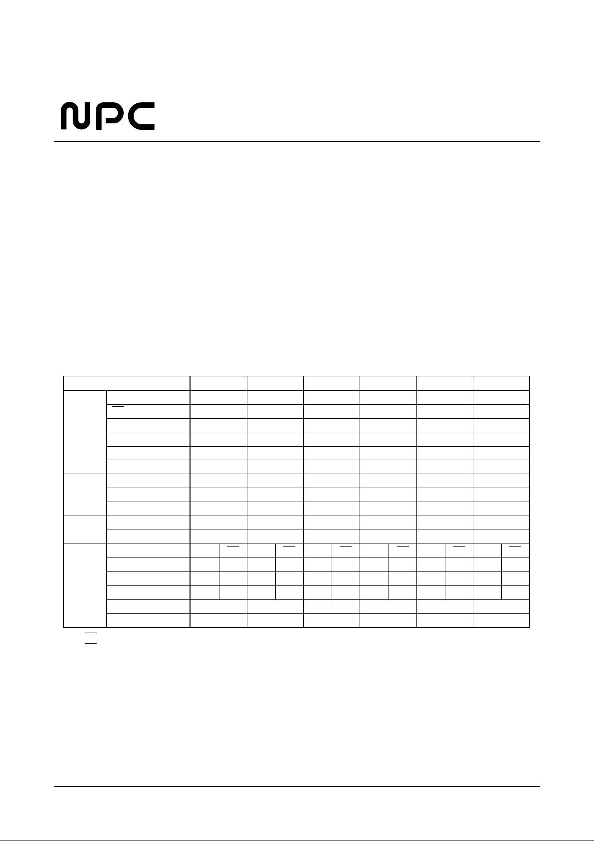
CF5732EA CF5732FA CF5732GA CF5732HA CF5732JA CF5732KA
Built-in XT terminal C
G(pF) 11.5 11.5 10 11.5 11.5 11.5
Capacitor XT terminal C
D(pF) 29 29 25 29 29 29
C1(pF) 6 6 3666
C2(pF) 7 7 4777
C4(pF) 8 8 5888
C4(pF) 9 9 6999
Motor Active Level - H L H H H
Output Hand Drive Cycle(sec) 0.125 1 1111
Pulse Width(msec) DUTY50% 31.25 31.25 15.6 23.4375 46.875
Alarm Active Level L L LLLL
Input Test Function Yes(1/2V
DD) Yes(1/2VDD) Yes(1/2VDD) Yes(1/2VDD) Yes(1/2VDD) Yes(1/2VDD)
Alarm Terminal AO AO AO AO AO AO AO AO AO AO AO AO
Output Active Level H L(*1) H L(*2) H L(*1) H L(*2) H L(*2) H L(*2)
Fundmental Frequency(Hz) 2048 2048 2048 2048 2048 2048 2048 2048 2048 2048 2048 2048
Modulation Frequency(Hz) 8+1 8+1 8+1 8+1 8+1 8+1 16+116+18+18+18+18+1
I
OH MIN(mA) −1.0 −1.0 −1.0 −1.0 −1.0 −1.0
I
OL MIN(mA) 1.0 1.0 1.0 1.0 1.0 1.0
(*1) AO is the reverse phase of AO, when output is active. (the same phase, when output is inactive)
(*2) AO is complete reverse phase of AO. (even output is inactive.)

NIPPON PRECISION CIRCUITS-2
CF5732 Series
PINOUT
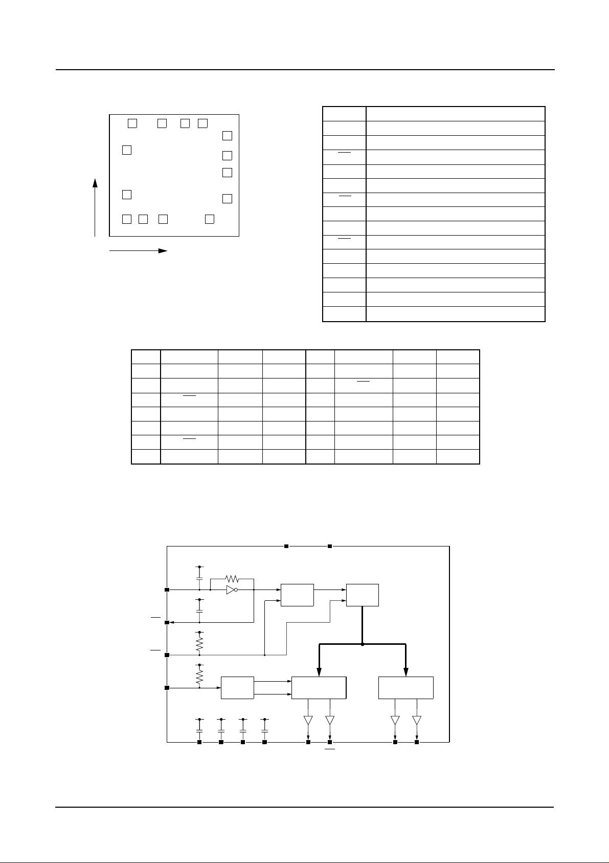
(0, 0)
1234
5
6
78 9
11
X
Y
10
12
13
14
Name
VDD
VSS
TC
AI
AO
AO
OUT2
OUT1
XT
XT
C1
C2
C3
C4
Description
Power supply pin
Ground
Test pin
Alarm Input
Alarm signal Output
Alarm signal Inverting Output
Motor drive output 2
Motor drive output 1
Crystal oscillator connection
Crystal oscillator connection
Supplementary internal capacitor connection 1
Supplementary internal capacitor connection 2
Supplementary internal capacitor connection 3
Supplementary internal capacitor connection 4
Chip size: 1.49×1.40mm
Chip thickness: 300±30µm
Pad size: 100×100µm
Reverse side of chip is VDD.
No Name X Y No Name X Y
1 VDD 1023 1248 8 OUT1 340 151
2 VSS 817 1248 9 XT 567 151
3 TC 553 1248 10 XT 1101 151
4 AI 214 1248 11 C1 1305 382
5 AO 151 943 12 C2 1305 682
6 AO 151 429 13 C3 1305 880
7 OUT2 151 151 14 C4 1305 1105
(Unit: µm)
PIN DESCRIPTION
BLOCK DIAGRAM
4 Stage
Divider
13 Stage
Divider
Alarm
Input
Alarm Output
Control
Mortor Output
Control
VDD
VSS
AO AO OUT1 OUT2
TC
AI
Alarm
Test
XT
CG
CD
XT
C1 C2 C3 C4
 Loading...