NPC CF5705CG, CF5705CF, CF5705BC, CF5705AE, CF5705AD Datasheet
...
pF
−
××
CF5705 series
NIPPON PRECISION CIRCUITS INC.
Analog Watch Stepping Motor Driver
OVERVIEW
The CF5705 series is a low-current analog watch stepping motor driver CMOS IC with built-in 32.768 kHz
crystal oscillator circuit.
FEATURES
■
32.768 kHz crystal oscillator circuit
C
and C
G
■
3.6 to − 1.2 V operating supply voltage range
built-in
D
■
Operating current consumption
•V
= –1.55V, C
SS
•V
= –2.8V, C
SS
Note: Current consumption depends on the built-in capacitor.
■
Reset function
= 16pF: 250 nA (max)
D
= 26pF: 1000 nA (max)
D
4 Hz and subsequent frequency dividers are reset
SERIES LINEUP
Pad coordinates Motor
Version
12345678
CF5705AA XT XTN RESET VSS TEST OUT2 OUT1 VDD 1 4.9m 125m 4 16
CF5705BC VSS RESET XT XTN VDD OUT2 OUT1 TEST 250m 23.4m 125m 4 26
CF5705AD XT X TN RESET VSS TEST OUT2 OUT1 VDD 1 23.4m 125m 4 30
CF5705AE XT XTN RESET VSS TEST OUT2 OUT1 V DD 20 5.9m 125m 4 16
CF5705CF VSS TEST XTN XT V DD OUT2 OUT1 RESET 1 4.9m 62.5m 4 16
CF5705CG VSS TEST XTN XT VD D OUT2 OUT1 RESET 1 3.9m 62.5m 4 16
1. Parasitic capacitance is included. Parasitic capacitance: C
G
= C
= 4pF
D
Cycle
(Tcy/2)
sec
Pulse
(Tpw)
sec
Test
(Tcy)
sec
Built-in
capacitor
C
G
pF
1
C
D
PART NUMBER GUIDE
CF5705
ORDERING INFORMATION
De vice Pack ag e
CF5705
Chip form
Function(Motor, Built-in capacitor)
Pad coordinate
NIPPON PRECISION CIRCUITS—1

×
µ
µ m)
CF5705 series
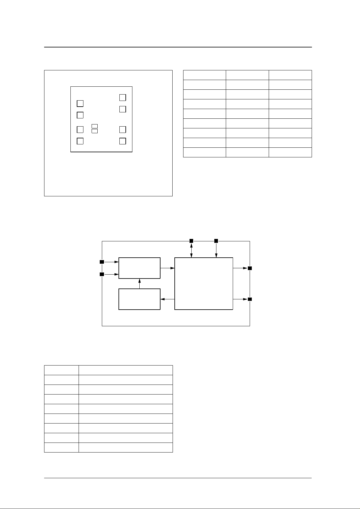
PAD DIMENSIONS
NPC
HA5705
1
2
3
4
(0,0)
Chip size: 1.000
Chip thickness: 220 µ m
Pad size: 100 × 100 µ m
Re verse side: V
BLOCK DIAGRAM
(Top view)
(1000,1060)
8
7
6
5
1.060 mm
level
DD
PAD COORDINATES
Number X (
1 155 785
2 155 597
3 155 363
4 155 175
5 844 175
6 844 363
7 844 694
8 844 882
TESTRESET
m) Y (
XT
XTN
PAD DESCRIPTION
Name Description
VS S Negative supply voltage
V DD Positive supply voltage
X T Crystal oscillator circuit input
X TN Cr ystal oscillator circuit output
OUT1 Stepping motor driver output 1
OUT2 Stepping motor driver output 2
RESET Reset input
TEST Test mode select. 512 Hz clock output
32kHz
Oscillator
Voltage
regulator
OUT1
Divider and
Output buffer control
OUT2
Pin number: Refer to Series lineup.
NIPPON PRECISION CIRCUITS—2

−
−
−
° C
−
−
−
° C
−
CF5705 series
SPECIFICATIONS
Absolute Maximum Ratings
V
= 0 V
DD
Parameter Symbol Rating Unit
Supply voltage range V
Input voltage range V
Storage temperature range T
Recommended Operating Conditions
Parameter Symbol Rating Unit
Supply voltage V
Operating temperature T
−
−
−
−
−
∆
ε
ε
SS
IN
stg
SS
opg
5.0 to 0.3 V
V
0.3 to 0.3 V
SS
40 to 125
3.6 to
1.2 V
20 to 75
Electrical Characteristics
V
= 0 V, T
DD
Operating supply voltage V
Operating current consumption
Reset input current I
Reset input resistance R
Motor output current I
Motor output cycle time
Motor output cycle time
Motor output pulsewidth
Oscillator start voltage
Oscillator start time T
Frequency voltage deviation
Frequency deviation
Internal capacitance
1. Current consumption is measured in the measurement circuit (see next page).
2. Ref er to Series lineup.
3. ε ’ = [f (1.55V) – f’
’ = [f (2.8V) – f’
f’
: Oscillation frequency center value of Standard Deviation in the same measuring conditions
0
= 25 ° C, X’tal C
a
= 55k Ω max
I
Parameter Symbol Condition
SS
2
(normal mode)
2
(test mode) t
2
2
3
2
] / f’
(C
= 16pF)
0
0
D
] / f’
(C
= 26pF)
0
0
D
No load, V
(C
1
I
DD
TR
No load, V
(C
TR
RESET: V
1.55V
RST
RESET: V
V
RST
V
RST
R
L
R
L
From supply ON to 512 Hz output
on TEST
f/f V
SS
MOT
T
T
V
RST
CY
CY
PW
STA
STA
Built-in C
’
Built-in C
C
, C
(C
G
D
G
= –1.55V,
SS
+ C
) = 15 pF, C
G
+ C
G
=
1.35 V, V
=
2.6 V, V
= 2 k Ω , V
= 1 k Ω , V
SS
) = 24 pF, C
RST
RST
D
= –2.8V,
D
= V
, V
DD
= V
, V
DD
= –1.55V 15 35 60 k Ω
SS
= –2.8V 5 15 5 0 k Ω
SS
=
1.55 V 0.7 – – m A
SS
=
2.4 V 2.18 2.29 – m A
SS
= − 1.2 → − 3.6 V, C
D
and C
D
G
+ C
) < 62 pF Refer to the SERIES LINEUP pF
D
= 16 pF
= 26 pF
= –
SS
= –2.8V – 25 10 0 nA
SS
= 5 pF – 0.2 1 ppm/0.1V
TR
Rating
Unit
min typ max
2.0
−−
1.2 V
– 0.15 0.25 µA
– 0.40 1.00 µA
–6–nA
s
Refer to the SERIES LINEUP
ms
ms
1.3 – – V
–25s
– 8 – 8 ppm
– 16 – 16 ppm
NIPPON PRECISION CIRCUITS—3
 Loading...