

×
SM5050A
NIPPON PRECISION CIRCUITS INC.
Single-output Clock Generator IC
OVERVIEW
The SM5050A is a single-output clock generator IC that generates standard high-frequency clocks derived
from a 20 to 40MHz crystal oscillator master clock. The high-frequency output stage uses optimized PLL circuits for low jitter output. The oscillator capacitors C
and C
G
are built-in, realizing a high-frequency output
D
oscillator by just the connection of a crystal. Two program inputs allows selection from 4 frequency multipliers, making the SM5050A able to generate multi-standard frequency clock outputs.
FEATURES
■
2.7 to 3.6V operating supply voltage
■
20 to 40MHz master clock frequency (fundamental)
■
Output frequency ranges
• 100 to 166.6MHz (V
• 100 to 125MHz (V
■
8mA output drive capability
■
Oscillator capacitors (C
tor (R
) built-in
■
■
■
■
f
100ps (typ) low jitter output (peak-to-peak)
2 program inputs for 4 selectable multiplier ratios
Standby function
Packaging
DD
DD
= V
G
= V
, C
= 3.0 to 3.6V)
DDQ
= 2.7 to 3.6V)
DDQ
) and feedback resis-
D
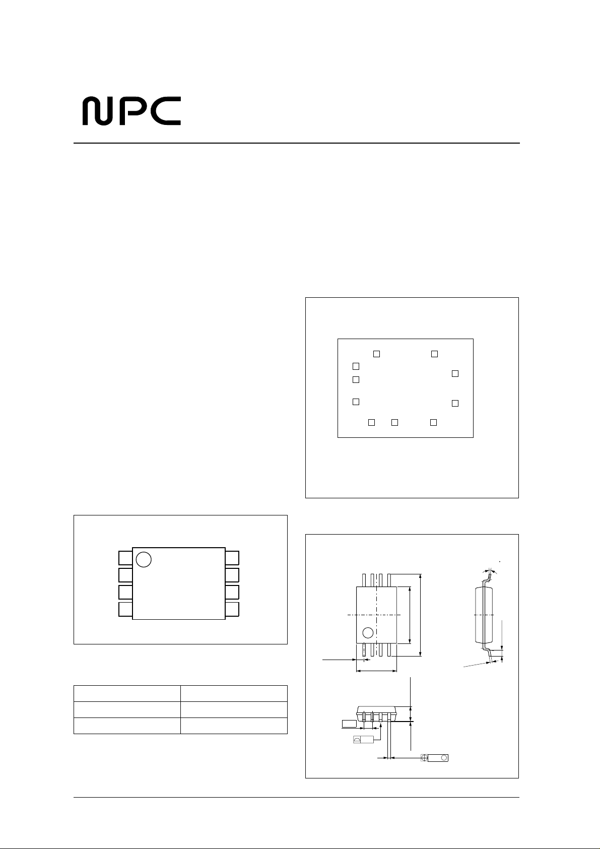
PAD DIMENSIONS
(Unit: µm)
P1 P0
VSS
VSSQ
Q
SA5050A
(0,0)
VDDQ
VDD XTN
(2160,1570)
INHN
XT
• Chip form (CF5050A)
• 8-pin VSOP package (SM5050AV)
Chip size: 2.16
Chip thickness: 300 ± 30µm
Chip base: V
1.57mm
level
SS
PINOUT
(Top view )
1P1
2VSS
3Q
VDD
4
ORDERING INFORMATION
De vice Pack ag e
CF5050A–1 Chip form
SM5050AV 8-pin VSOP
8P0
7 INHN
6XT
5
XTN
PACKAGE DIMENSIONS
(Unit: mm )
6.4 ± 0.3
4.4 ± 0.2
0.575 typ
3.1 ± 0.3
1.15 ± 0.05
0.65
0.10
0.1 ± 0.05
0.22 ± 0.1
NIPPON PRECISION CIRCUITS—1
0.12
0 to 10
0.5 ± 0.2
0.1
+
0.05
−
0.15
M
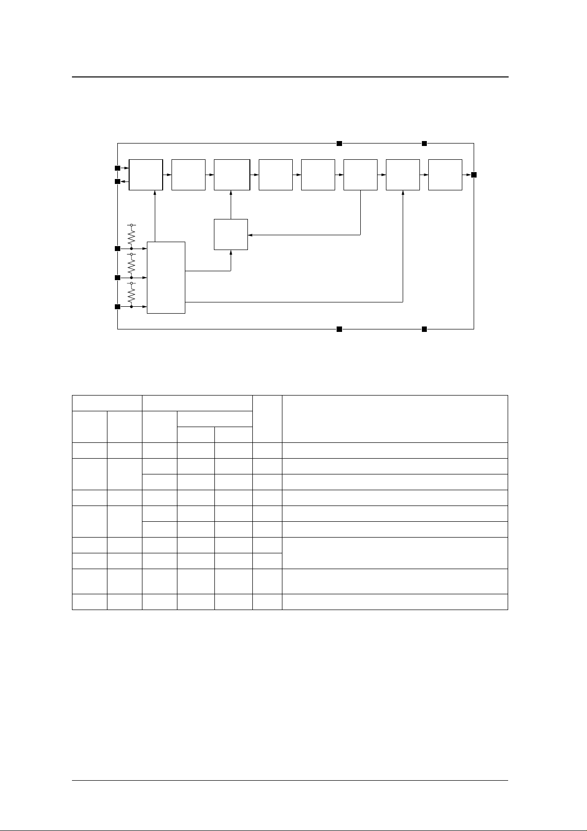
BLOCK DIAGRAM
SM5050A
VDDQ
Duty
Control
Circuit
VSSQVSS
XT
XTN
P0
P1
INHN
Oscillator R-counter
Control
Circuit
Phase
Detector
N-counter
Charge
Pump
VDD
LPF Q
VCO
PIN DESCRIPTION
SM5050AV CF5050A
1
Number Name Name
1 P1 P1 620 1330 Ip Program input 1. Selects the output frequency multiplier ratio.
2 VSS
VSSQ 290 920 – Output circuit ground
3 Q Q 290 5 69 O Output (CMOS)
VDDQ 540 240 – Output circuit supply
4 VDD
5 X TN X TN 1524 240 O
6 XT X T 1870 542 I
7 INHN INHN 1870 1015 Ip
8 P0 P0 1540 1330 Ip Program input 0. Selects the output frequency multiplier ratio.
1. Ip = input with built-in pull-up resistor.
Pad dimensions [µm]
XY
VS S 290 1132 – Ground
VD D 906 240 – Supply
I/O
Cr ystal oscillator connection pins.
Crystal connected between XT and XTN.
Op erating state control (inhibit).
When INHN is LOW, output is high impedance and PLL circuits stop.
Description
Output
Buffer
NIPPON PRECISION CIRCUITS—2

×
×
×
×
−
−
−
−
°
−
°
−
°
OUTPUT FREQUENCY SETTINGS
−
°
SM5050A
Program inputs
P0 P1
LOW LOW
Multiplier ratio
4 25.00 100
4.25 25.00 106.25
Master clock
frequency [MHz]
Output frequency
[MHz]
Supply voltag e [V]
2.7 to 3.6LOW HIGH
25.00 125
HIGH LOW
5
26.66 133.3
HIGH HIGH
6.25
24.8832 155.52
3.0 to 3.6
26.66 166.6
Note: The output frequency range is 100 to 166.6MHz. The master clock frequency can be adjusted to any value within the range 20 to 40MHz,
so the master clock frequency and multiplier should be selected such that the output frequency is within the output frequency range.
SPECIFICATIONS
Absolute Maximum Ratings
V
= 0V
SS
Parameter Symbol Condition Rating Unit
Supply voltage range V
Input voltage range V
Output voltage range V
Storage temperature range T
Operating temperature range T
Output current I
Po w er dissipation P
DD
IN
OUT
CF5050A
stg
SM5050AV
opr
OUT
SM5050AV 150 m W
D
0.5 to 6.0 V
0.5 to V
0.5 to V
+ 0.5 V
DD
+ 0.5 V
DD
65 to 150
55 to 125
40 to 85
25 mA
C
C
C
Recommended Operating Conditions
V
= 0V, f
SS
Operating supply voltage V
Input voltage V
Operating temperature T
= 100 to 166.6MHz, C
OUT
= 15pF
L
Parameter Symbol Condition
f
≤ 125MHz 2.7 – 3.6
OUT
DD
f
≤ 166.6MHz 3.0 – 3.6
OUT
IN
opr
Rating
min typ max
V
SS
–V
DD
20 – 80
NIPPON PRECISION CIRCUITS—3
Unit
V
V
C
 Loading...