NOVATEK NT6881H, NT6881 Datasheet

NT6881
USB Keyboard Micro-Controller
1 V2.6
Features
n Built-in 6502 8-bit CPU
n 3 MHz CPU operation frequency when oscillator is
running at 6 MHz
n 6K bytes of ROM
n 256 bytes of SRAM
n One 8-bit programmable base timer with pre-divider
circuit
n 29 programmable bi-directional I/O pins including two
external interrupts
n 3 LED direct sink pins with internal serial resistors
n On-chip oscillator (Crystal or Ceramic Resonator)
n Watch-dog timer reset
n Built-in power on reset
n USB interface
n 3 Endpoints provided
n Remote Wakeup provided
n CMOS technology for low power consu mption
n 40-pin DIP package, 42-pad Chip Form and COB
General Description
The NT6881 is a single chip micro-controller for USB
keyboard applications. It incorporates a 6502 8-bit CPU
core, 6K bytes of mask ROM, and 256 bytes of RAM used
as working RAM and stack area. It also includes 29
programmable bi-directional I/O pins with built-in
resistors, and one 8-bit pre-loadable base timer.
Additionally, it includes a built-in power-on reset, a builtin low voltage reset, an oscillator that requires crystal or
ceramic resonator applied, and a watch-dog timer that
prevents system standstill.
Pin Configuration
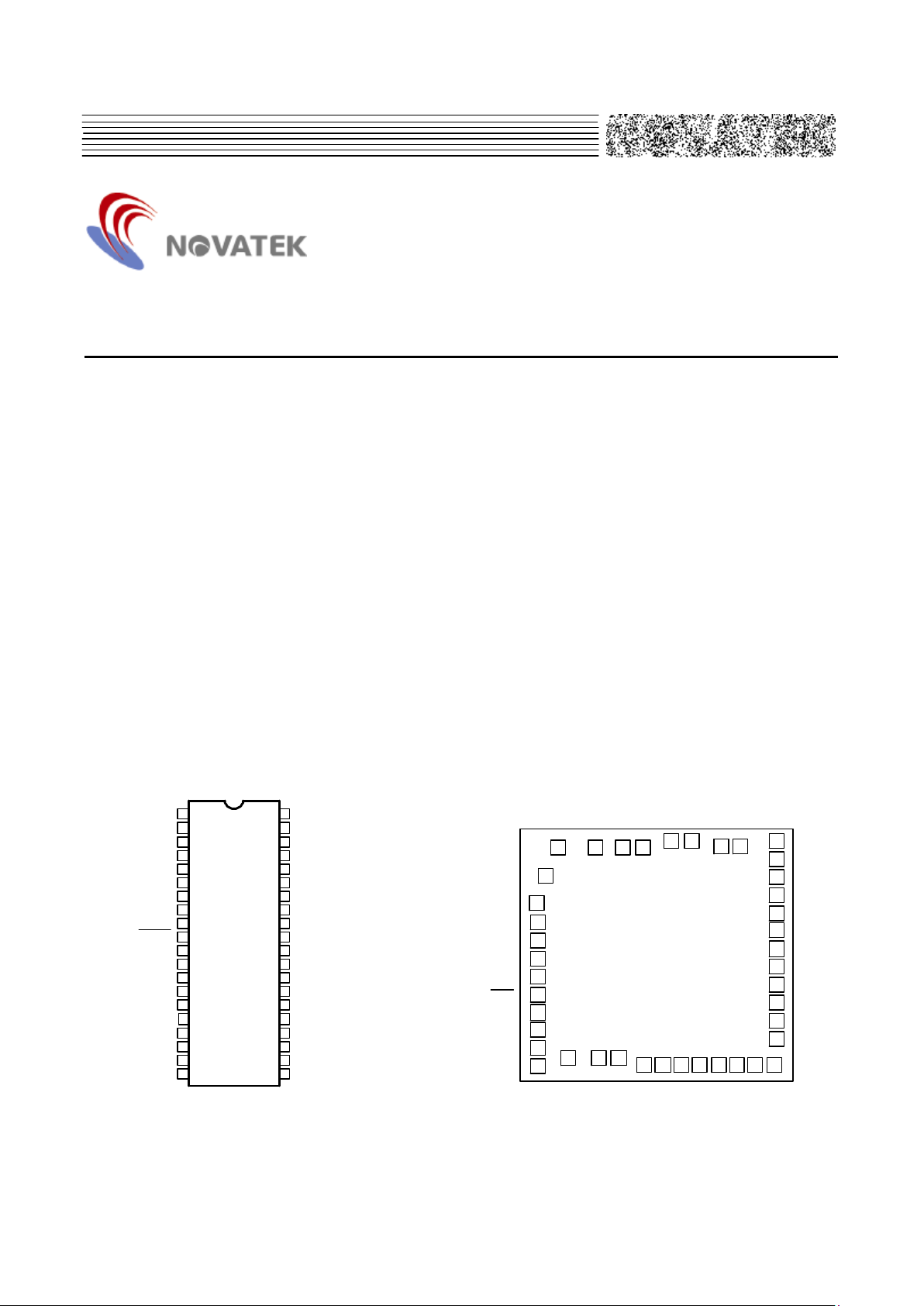
GND
VCP
VDP
VDM
P30
P31
INT0/P32
INT1/P33
P34
P11
P00
P02
P03
P17 P04
P20
P21
P22
P23
P25
P26
LED0
LED1
V
DD
LED2
OSCO
OSCI
P12
P27
NT6881
1
2
3
4
5
6
7
8
9
10
11
12
13
14
15
16 25
26
27
28
29
30
31
32
33
34
35
36
37
38
39
40
RESET
P01
P05
P06
P07
P10
17
18
19
20
P24
P16
P15
P14
P13
24
23
22
21
Pad Configuration
2625
181716
15
14
4 3 2 1
42 41
40 39
P
1
0
P
1
1
P
1
2
P
1
3
P
1
4
P
0
6
P
0
5
P
0
4
P20
P21
P22
P23
P24
P25
P26
P27
LED0
LED1
LED2
VDM
P30
P31
P32
P33
P34
RESET
P00
P01
P02
V
D
P
V
C
P
G
N
D
G
N
D
O
S
C
I
O
S
C
O
V
C
C
V
C
C
P
0
7
13
12
11
10
9
8
7
5
35
36
37
38
31
32
33
34
27
28
29
30
242322212019
P03
6
P
1
5
P
1
6
P17
NT6881H

NT6881
2
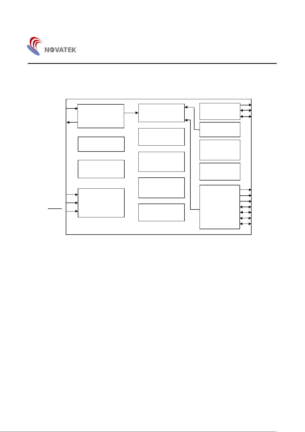
Block Diagram
Power Down/Up
6K Bytes
Mask ROM
6502
CPU
Interrupt
Controller
Base Timer
Watch Dog
Timer
256 Bytes
SRAM
SIE
FIFOs
Serial Bus
Manager
VCP
VDP
VDM
LED0
LED1
LED2
P00~P07
P10~P17
P20~P27
P30~P34
OSCI
OSCO
VDD
GND
RESET
Timing Generator
Power-On
Reset
Transceiver
I/O PORTs

NT6881
3
Pin and Pad Descriptions
Pin No. Pad No. Designation I/O Description
1 1,2 GND P Ground
2 3 VCP O USB 3.3V driver
3 4 VDP I/O USB data plus
4 5 VDM I/O USB data minus
6 Bi-directional I/O 5
P30 I/O
Program output enable
7 I/O Bi-directional I/O 6
P31
Program control
7 8 P32/INT0 I/O Bi-directional I/O shared with INT0
8 9 P33/INT1 I/O Bi-directional I/O shared with INT1
9 10 P34 I/O Bi-directional I/O
11
RESET
I Internally pulled down resistor 10
Program supply voltage
12~19 P00 ~ P07 I/O Bi-directional I/O 11 ~ 18
Program address buffer
20~24 P10 ~ P14 I/O Bi-directional I/O 19 ~ 23
Program address buffer
25 P15 I/O Bi-directional I/O 24
Program chip enable
25 ~ 26 26~27 P16 ~ P17 I/O Bi-directional I/O
28~35 P20 ~ P27 I/O Bi-directional I/O 27 ~ 34
Program data buffer
36 LED0 O LED direct sink 35
Mode selection
37 LED1 O LED direct sink 36
Mode selection
38 LED2 O LED direct sink 37
Mode selection
38 39,40 VDD P Power supply (+5V)
39 41 OSCO O Crystal oscillator output
40 42 OSCI I Crystal oscillator input

NT6881
4
Functional Description
1. 6502 CPU
The 6502 is an 8-bit CPU that provides 56 instructions, decimal and binary arithmetic, thirteen addressing modes,
true indexing capability, programmable stack pointer and variable length stack, a wide selection of addressable
memory range, and interrupt input. Other features are also included.
The CPU clock cycle is 3MHz (6MHz system clock divided by 2). Please refer to 6502 data sheet for more
detailed information.
Accumulator A
Index Register Y
07
7
Index Register X
7 0
0
Stack Pointer SP
0
N Status Register P
07
Carry
Zero
IRQ Disable
Decimal Mode
BRK Command
Overflow
Negative
7
Program Counter PCH
815
7 0
PCL
1 = TRUE
1 = Result ZERO
1 = DISABLE
1 = TRUE
1 = NEG
1 = TRUE
1 = BRK
V B D I Z C
Figure 1.1. 6502 CPU Registers and Status Flags

NT6881
5
2.Instruction Set List
Instruction Code
Meaning Operation
ADC Add with carry A + M + C → A,C
AND Logical AND A•M → A
ASL Shift left one bit C ← M7•••M0 ← 0
BCC Branch if carry clear Branch on C=0
BCS Branch if carry set Branch on C=1
BEQ Branch if equal to zero Branch on Z=1
BIT Bit test A•M,M7 → N,M6 → V
BMI Branch if minus Branch on N=1
BNE Branch if not equal to zero Branch on Z=0
BPL Branch if plus Branch on N=0
BRK Break Forced interrupt PC + 2↓ PC↓
BVC Branch if overflow clear Branch on V=0
BVS Branch if overflow set Branch on V=1
CLC Clear carry 0 → C
CLD Clear decimal mode 0 → D
CLI Clear interrupt disable bit 0 → I
CLV Clear overflow 0 → V
CMP Compare accumulator to memory A - M
CPX Compare with index register X X - M
CPY Compare with index register Y Y - M
DEC Decrement memory by one M - 1 → M
DEX Decrement index X by one X - 1 → X
DEY Decrement index Y by one Y - 1 → Y
EOR Logical exclusive -OR A ⊕ M→A
INC Increment memory by one M + 1 → M
INX Increment index X by one X + 1 → X
INY Increment index Y by one Y + 1 → Y
JMP Jump to new location (PC + 1) → PCL,(PC + 2) → PCH
JSR Jump to subroutine PC + 2↓,(PC + 1) → PCL,(PC + 2) → PCH

NT6881
6
Instruction Set List (contiuned)
Instruction Code
Meaning Operation
LDA Load accumulator with memory M → A
LDX Load index register X with memory M → X
LDY Load index register Y with memory M → Y
LSR Shift right one bit 0 → M7•••M0 → C
NOP No operation No operation (2 cycles)
ORA Logical OR A + M → A
PHA Push accumulator on stack A ↓
PHP Push status register on stack P ↓
PLA Pull accumulator from stack A ↑
PLP Pull status register from stack P ↑
ROL Rotate left through carry C ← M7•••M0 ← C
ROR Rotate right through carry C → M7•••M0 → C
RTI Return from interrupt P ↑,PC ↑
RTS Return from subroutine PC ↑,PC+1 → PC
SBC Subtract with borrow A - M - C → A,C
SEC Set carry 1 → C
SED Set decimal mode 1 → D
SEI Set interrupt disable status 1 → I
STA Store accumulator in memory A → M
STX Store index register X in memory X → M
STY Store index register Y in memory Y → M
TAX Transfer accumulator to index X A → X
TAY Transfer accumulator to index Y A → Y
TSX Transfer stack pointer to index X S → X
TXA Transfer index X to accumulator X → A
TXS Transfer index X to stack pointer X → S
TYA Transfer index Y to accumulator Y → A
* For more detailed specifications, please refer to 6502 programming data book.

NT6881
7
3. Mask ROM: 6K X 8 bits
The built-in mask ROM program code, executed by the 6502 CPU, has a capacity of 6K X 8-bit and is addressed from
E800H to FFFFH.
4. SRAM: 256 X 8 bits
The built-in SRAM is used for general purpose data memory and for stack area. SRAM is addressed from 0080H to
017FH. Because the 6502 default stack pointer is 01FFH, the stack area will map $01FF-$0180 to $00FF-$0080, thus the
programmer can set “S” register to 7FH when starting program, allowing stack point is 017FH.
as; LDX #$7F
TXS
System Registers
Unused
RAM
RAM
Unused
ROM
$FFFA
$FFFB
$FFFC
$FFFD
$FFFE
$FFFF
NMI Vector
RESET Vector
IRQ Vector
stack pointer
$0000
$001F
$0080
$00FF
$0100
$017F
$E800
NMI-L
NMI-H
RST-L
RST-H
IRQ-L
IRQ-H
 Loading...