NOVATEK NT6880, NT6880H Datasheet

Features
Built-i n 6502 8- bi t CPU
2 MHz CPU operation frequency
5K bytes of ROM
160 bytes of SRAM
One 8-bit programmabl e base tim er wit h
1 - 256 µsec interval
29 programmable bi-dir ecti onal I/O pins
3 LED direct sink pins
General Description
The NT6880 is a single chip micro-controller for
keyboard applications. I t incorporates a 6502 8-bit CPU
core, 5K bytes of ROM and 160 bytes of RAM used as
working RAM and stack area. It also includes 29
programm able bi-directional I/O pins and one 8-bit pre-
NT6880
Keyboard Controller
Mask optional for built-in RC oscillator with an
external resistor or external ceramic resonator applied
Mask optional for DATA/CLK driv i ng capability
Watc h- dog t i mer reset
Built-in power-on reset
Built-in low voltage reset
CMOS technology for low power consumption
Available in 40 pin DIP package and 40 pad Chip
Form
loadable base timer. Additionally, it includes a built-in
low voltage reset, a 4MHz RC oscillator requiring an
externally applied resistor or a 4MHz ceramic resonator
and a watch-dog timer that prevents system standstill.
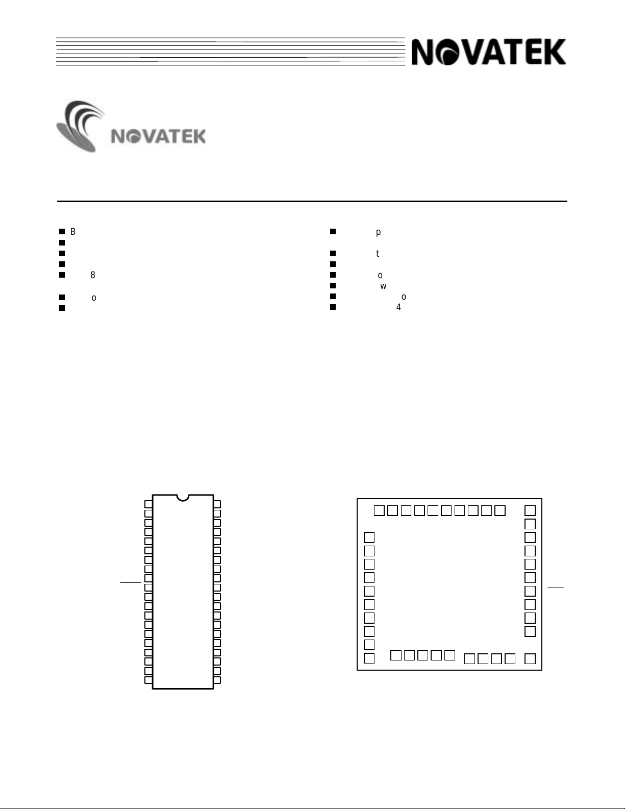
Pin Configuration
GND
NC
DATA
CLK
P30
P31
P32
P33
P34
RESET
P00
P01
P02
P03
P05
P06
P07
P10
P11
1
2
3
4
5
6
7
8
9
10
11
12
13
14
15
40
39
38
37
36
35
34
33
NT6880
32
31
30
29
28
27
26
16 25
17
18
19
20
24
23
22
21
OSCI
R/OSCO
V
DD
LED2
LED1
LED0
P27
P26
P25
P24
P23
P22
P21
P20
P17P04
P16
P15
P14
P13
P12
Pad Configuration
P
P
1
1
6
7
26 25 24 23 22 21 20 19 18 17
27
P20
28
P21
29
P22
30
P23
31
P24
32
P25
33
P26
34
P27
35
LED0
36
LED1
L
E
D
2
P
1
5
V
D
D
P
P
1
1
3
4
NT6880H
40393837
O
R
S
/
C
O
I
S
C
O
P
1
1
1
2
1
G
N
D
1
0
NCD
0
0
6
7
P05
16
P04
15
14
P03
13
P02
12
P01
11
P00
10
RESET
9
P34
8
P33
7
P32
P31
6 5 4 3 2
C
P
A
L
3
T
K
0
A
P
P
P
P
1V1.0

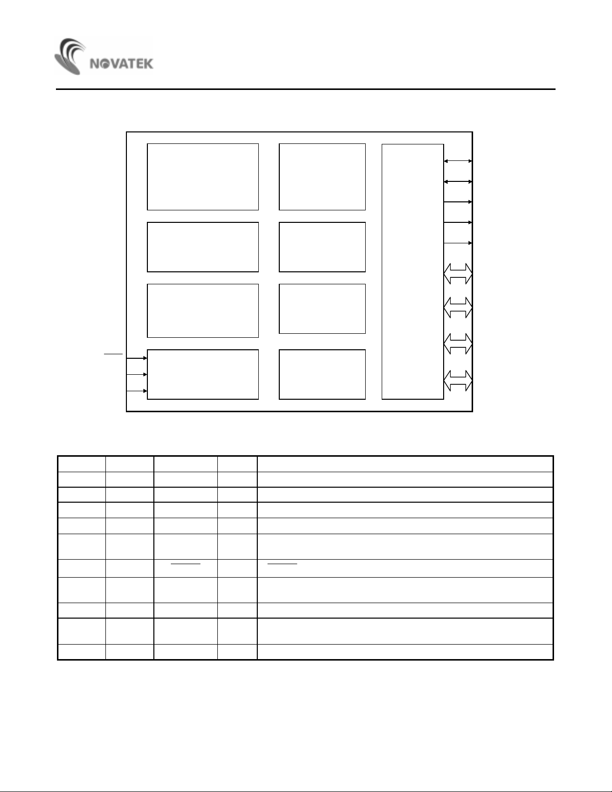
Block Diagram
Timing Generator
(RC OSC/Ceramic Resonator: 4MHz)
5K Bytes
ROM
NT6880
CLK
DATA
LED0
LED1
LED2
P00 - P07
P10 - P17
P20 - P27
P30 - P34
RESET
V
DD
GND
6502
CPU
Interrupt
Controller
Power-On RESET/
Low Voltage RESET
160 Bytes
SRAM + STACK
Watch Dog
Timer
Base Timer
I/O PORTs
Pin and P ad Descripti ons
Pin No. Pad No. Designation I/O Description
1 1 GND P Ground pin
2 2 NC - No connection, recommended to connect VDD or floati ng
3 3 DATA I/O
4 4 CLK I/O
5 - 9,
11 - 34
10 10
35 - 37 35 - 37 LED0 -
5 - 9,
11 - 34
P30 - P34,
P00 - P27
RESET
I/O Bi-directional I/O pins
O LED direct sink pins
LED2
38 38 V
DD
P Power supply
39 39 R/OSCO I
40 40 OSCI - No connection for RC OSC connected for 4MHz ceramic resonator
I/O, 10KΩ pull-up resistor for communication
I/O, 10KΩ pull-up resistor for communication
I
RESET
signal input pi n wi t h internal pull up resist or ; Act i ve low
47KΩ resistor connected for RC OSC or 4MHz cerami c r esonator
connected
* Under the constraint of t he maxim um fr equency variation, (∆F/F)
be selected and pin 39 and pin 40 must be connected to a ceramic resonator. If (∆F/F)
, ≤ ±1%, code 3, 7 (ceramic resonator option) m ust
max
, ≤ ±10%, code 1, 5 (RC OSC
max
option) it i s r ecom mended that pin 39 be connected to a 47KΩ resistor with ≤ ±1% accuracy to V
2
DD
. Pin 40 is fl oating.

Functional Description
1. 6502 CPU
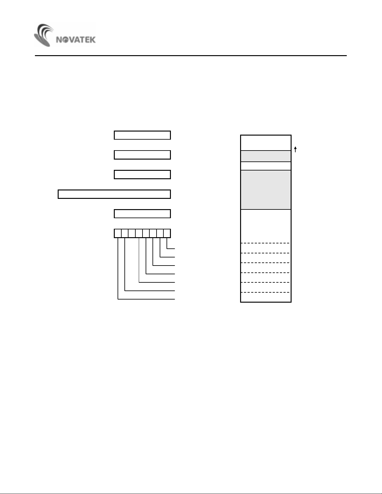
The 6502 is an 8-bit CPU. Please refer to the 6502 data sheet for more details.
70
ACCUMULATOR A
70
INDEX REGISTER X
70
INDEX REGISTER Y
0000
009F
00C0
SYSTEM REGISTERS
00CF
SRAM
UNUSED
NT6880
STACK PTR
15 0
PROGRAM COUNTER PC
70
S
70
S V B D I Z C
STACK POINTER SP
STATUS REGISTER P
CARRY
ZERO
INTERRUPT MASK
DECIMAL MODE
BREAK
OVERFOLW
SIGN
EC00
FFFA
FFFB
FFFC
FFFD
FFFE
FFFF
UNUSED
USER ROM
NMI-L
NMI-H
RST-L
RST-H
IRQ-L
IRQ-H
Figure 1.1 6502 CPU Registers and Stat us Fl ags Figure 1.2. NT6880 M emory Map
NMI VECTOR
IRQ VECTOR
3

NT6880
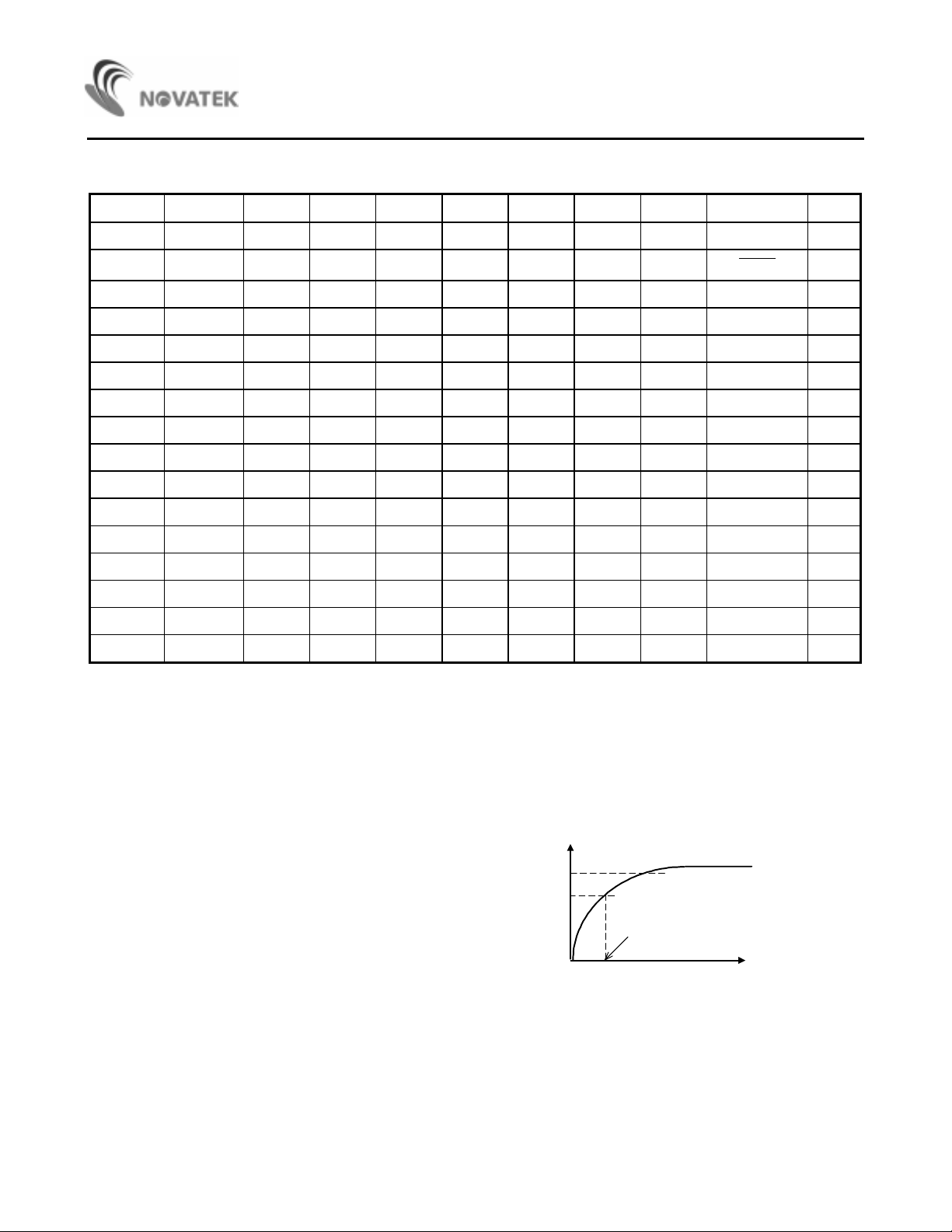
2. System Reserved Registers
Addr. Register Bit7 Bit6 Bit5 Bit4 Bit3 Bit2 Bit1 Bit0 R/W
$00C0 BT BT7 BT6 BT5 BT4 BT3 BT2 BT1 BT0 W
$00C1 TCON - - - - - - -
ENBT
$00C2 CLRIRQX - - - - - - - CLRIRQTMR W
$00C3 PORT0 PD07 PD06 PD05 PD04 PD03 PD02 PD01 PD00 RW
$00C4 PORT1 PD17 PD16 PD15 PD14 PD13 PD12 PD11 PD10 RW
$00C5 PORT2 PD27 PD26 PD25 PD24 PD23 PD22 PD21 PD20 RW
$00C6 PORT3 - - - PD34 PD33 PD32 PD31 PD30 RW
$00C7 CLK - - - - - - - CLK RW
$00C8 DATA - - - - - - - DATA RW
$00C9 LED - - - - - LED2 LED1 LED0 W
$00CA CLRWDT 0 1 0 1 0 1 0 1 W
$00CB X X X X X X X X X X
$00CC X X X X X X X X X X
$00CD X X X X X X X X X X
$00CE X X X X X X X X X X
$00CF X X X X X X X X X X
- : no effect X : access not allowed
W
3. ROM: 5K X 8 bit s
The built-in ROM program code, executed by the 6502
CPU, has a capacity of 5K X 8 bits and is addressed from
EC00H
to
FFFFH
.
4. SRAM: 160 X 8 bits
The built-in SRAM is used for general purpose data
memory and f or the stack area. SRAM is addressed from
0000H to
009FH
. User can allocate stack area in the
SRAM by setting stack pointer register (S). Because the
6502 default stack pointer is 01FFH, it must be mapped to
009FH
. Mapping from 01XX to 00XX is done internall y by
setting the S register to
9FH
via software program ming.
For example :
LDX #$9F
TXS
For compatibility to UM6868A with 128-byte SRAM, the
user’s source code can not be changed.
For example :
LDX #$7F
TXS
5. Power-On Reset
Built-in power-on reset circui t can generate a 150ms pulse
to reset the entire chip. The beginning of the 150ms pul se
occurs at 60% of V
power
DD
V
60%
when powered o n.
DD
The start of 150ms pulse
t
Figure 5.1. Power-O n Reset Ti ming
4
 Loading...