NOVATEK NT6861U, NT6861 Datasheet

Features
NT6861
8-Bit Microcontroller for Monitor
n 40 pin DIP & 42 pin SDIP package
n Operating Voltage Range: 4.5V to 5.5V
n CMOS technology for low power consumption
n Crystal oscillator or ceramic resonator* available
n 6502 8-bit CMOS CPU core
n 8MHz operation of frequency
n 4/8/12/16/24K bytes ROM are available
n 256 bytes of RAM (which stores EDID for DDC1/2B)
n One 8-bit pre-loadable base timer
n 14 channels of 8 bit PWM outputs:
6 channel with 5V open drain and 8 channel with 12V
open drain
n 2 channel A/D converters with 6-bit re solution
General Description
NT6861 is a monitor component µC for auto-sync and
digital controlled applications. It contains a 6502
8-bit CPU core, 256 bytes of RAM used as working RAM
and stack area, 24K bytes of ROM maximum for
programming, 14-channel 8-bit PWM D/A converters, 2channel A/D converters for key detection saving I/O pins,
one 8 bit pre-loadable base timer, internal Hsync and
Vsync signals processor providing mode detection,
watch-dog timer preventing system from abnormal
operation, and an I2C bus interface.
n 24 bi-directional I/O port pins and 1 I/P pin
n Hsync/Vsync signal processor
n Hardware sync signals polarity & freq. evaluator
n Built-In I2C bus interface
n Supporting VESA DDC1/2B function
n Six-interrupt sources
- INTV (Vsync INT)
- INTE (External INT with rising edge trigger)
- INTMR (Timer INT )
- INTA (Slave Address Matched INT)
- INTD (Shift Register INT)
- INTS (SCL GO-LOW INT)
n Hardware watch-dog timer function
Users can store EDID data in the 128 bytes of RAM for
DDC1/2B, so that users can save the cost of dedicated
EEPROM for EDID. Half frequency output function can
save external one-shot circuit. All of these designs create
savings in component costs.
* The frequency deviation of ceramic resonator has
+/- 6% maximum.
1 V2.0
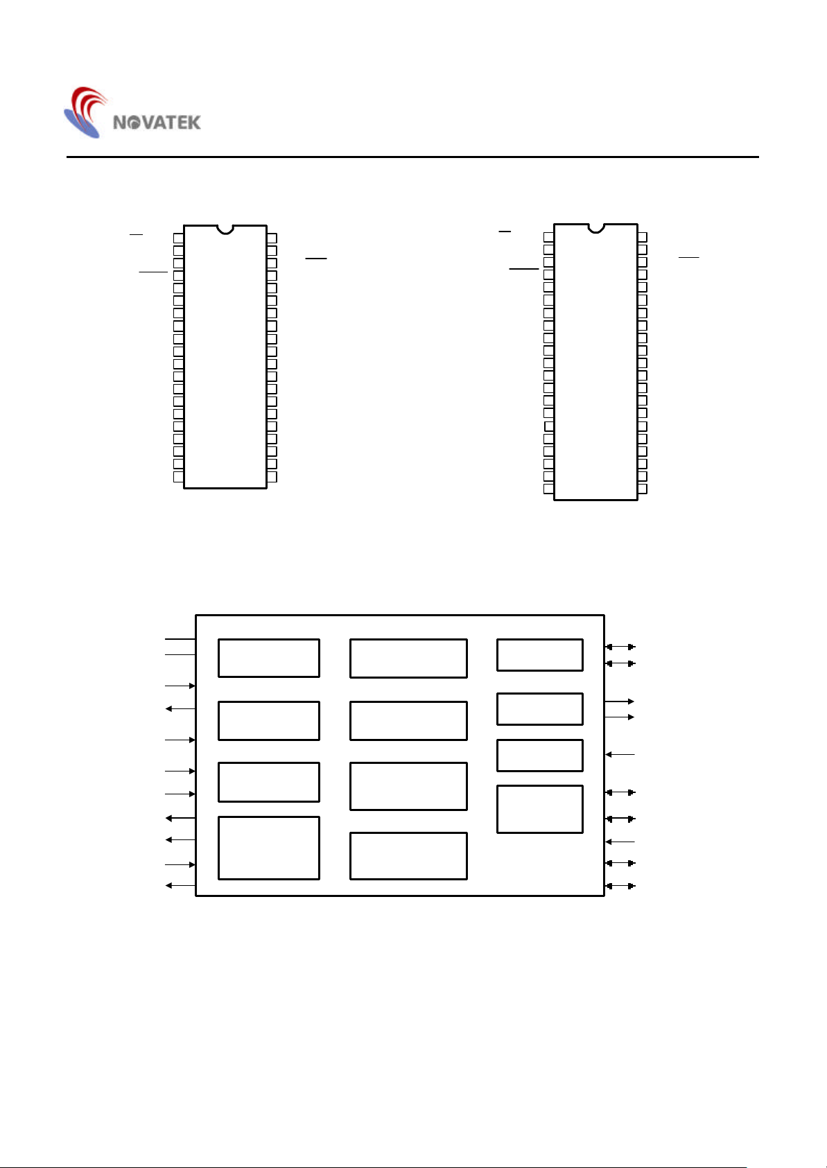
Pin Configuration
NT6861
[OE] DAC2
DAC1
DAC0
[VPP] RESET
V
GND
OSCO
OSCI
P15
[CE] P14
[A11] P13/HALFHI
[A10] P12/HALFHO
[A9] P11/AD1
[A8] P10/AD0
P16/INTE
[DB7] P27
[DB5] P25
[DB4] P24
[DB3] P23
Block Diagram
1
2
3
4
5
DD
6
7
8
NT6861
9
10
11
12
13
14
15
16 25
17
18
19
20
* [ ]: OTP Mode
VSYNCI/INTV/ [A14]
40
39
HSYNCI
38
DAC3 [PGM]
DAC4 [MODE0]
37
36
DAC5 [MODE1]
35
DAC6 [MODE2]
34
DAC7
P07/HSYNCO [A7]
33
32
P06/VSYNCO [A6]
31
P05/DAC13 [A5]
30
P04/DAC12 [A4]
29
P03/DAC11 [A3]
28
P02/DAC10 [A2]
27
P01/DAC9 [A1]
P00/DAC8 [A0]
26
P31/SCL [A13]
24
P30/SDA [A12][DB6] P26
23
P20 [DB0]
22
P21 [DB1]
21
P22 [DB2]
[OE] DAC2
DAC1
DAC0
[VPP] RESET
V
GND
OSCO
OSCI
P15
[CE] P14
[A11] P13/HALFHI
[A10] P12/HALFHO
[A9] P11/AD1
[A8] P10/AD0
[DB7] P27
[DB6]P26
[DB5] P25
[DB4] P24
[DB3] P23
1
2
3
4
DD
5
NC
6
7
8
9
10
11
12
13
14
15
16 27
17
18
19
20
21
* [ ]: OTP Mode
42
41
40
39
38
37
36
35
NT6861U
34
33
32
31
30
29
28
26
25
24
23
22
VSYNCI/INTV
HSYNCI
DAC3 [PGM]
DAC4 [MODE0]
DAC5 [MODE1]
NC
DAC6 [MODE2]
DAC7 [A14]
P07/HSYNCO [A7]
P06/VSYNCO [A6]
P05/DAC13 [A5]
P04/DAC12 [A4]
P03/DAC11 [A3]
P02/DAC10 [A2]
P01/DAC9 [A1]
P00/DAC8 [A0]P16/INTE
P31/SCL [A13]
P30/SDA [A12]
P20 [DB0]
P21 [DB1]
P22 [DB2]
VDD
GND
OSCI
OSCO
INTE
VSYNCI/INTV
HSYNCI
VSYNCO
HSYNCO
HALFHI
HALFHO
Timing Generator
CPU core
6502
Interrupt
Controller
H/V Sync Signals
Processor
Program ROM
4/8/12/16/24K Bytes
SRAM + STACK
256 Bytes
8 Bit Base Timer
Watch Dog Timer
IIC BUS
PWM DACs
SCL
SDA
DAC0 - DAC7
DAC8 - DAC13
A/D Converter AD0 - AD1
P00 - P07
I/O Ports
P10 - P15
P16
P20 - P27
P30 - P31
2

Pin Descriptions
NT6861
Pin No.
40 Pin 42 Pin
1 1 DAC2 O Open drain 12V, D/A converter output 2
2 2 DAC1 O Open drain 12V, D/A converter output 1
3 3 DAC0 O Open drain 12V, D/A converter output 0
4 4
5 5 V
6 7 GND P Ground
7 8 OSCO O Crystal OSC output
8 9 OSCI I Crystal OSC input
9 10 P15 I/O Bi-directional I/O pin
10 11 P14 I/O Bi- directional I/O pin
11 12 P13/HALFHI P13 I/O Bi- directional I/O pin, shared with half hsync input
12 13 P12/HALFHO P12 I/O Bi- directional I/O pin, shared with half hsync output
13 14 P11/AD1 P11 I/O
Designation Reset Init. I/O Description
RESET
DD
I Schmitt trigger input pin, low active reset*
P Power
Bi- directional I/O pin, shared with A/D converter channel
1 input
14 15 P10/AD0 P10 I/O
15 16 P16/INTE P16 I
16 - 23 17 - 24 P27 - P20 I/O
* This RESET pin must be pulled high by external pulled-up resistor (5KΩ suggestion), or it will stay low
voltage to reset system all the time.
Bi- directional I/O pin, shared with A/D converter channel 0
input
Schmitt trigger input pin with internal pull high, shared with
external Rising-edge trigger interrupt
Bi- directional I/O pin, push-pull structure with high current
drive/sink capability
3

Pin Descriptions (continued)
NT6861
Pin NO.
40 Pin 42 Pin
24 25 P30/SDA P30 I/O
25 26 P31/SCL P31 I/O
26 27 P00/DAC8 P00 I/O
27 28
28 29
29 30 P03/DAC11 P03 I/O
30 31
31 32
32 33
Designation Reset Init. I/O Description
P01/DAC9 P01 I/O
P02/DAC10 P02 I/O
P04/DAC12 P04 I/O
P05/DAC13 P05 I/O
P06/VSYNCO P06 I/O Bi- directional I/O pin, shared with vsync out
Open drain 5V Bi-direction I/O pin P30, shared with SDA pin of
I2C bus schmitt trigger buffer
Open drain 5V Bi-direction I/O pin P31, shared with SCL pin of
I2C
bus schmitt trigger buffer
Bi- directional I/O pin, shared with open drain 5V D/A converter
output 8
Bi- directional I/O pin, shared with open drain 5V D/A converter
output 9
Bi- directional I/O pin, shared with open drain 5V D/A converter
output 10
Bi- directional I/O pin, shared with open drain 5V D/A converter
output 11
Bi- directional I/O pin, shared with open drain 5V D/A converter
output 12
Bi- directional I/O pin, shared with open drain 5V D/A converter
output 13
33 34
34 35
35 36 DAC6 O Open drain 12V, D/A converter output
36 38
37 39 DAC4 O Open drain 12V, D/A converter output
38 40
39 41 HSYNCI I
40 42 VSYNCI/INTV VSYNCI I
- 6 NC
- 37 NC
P07/HSYNCO P07 I/O Bi-directional I/O pin, shared with hsync out
DAC7 O Open drain 12V, D/A converter output
DAC5 O Open drain 12V, D/A converter output
DAC3 O Open drain 12V, D/A converter output
Debouncing & Schmitt trigger input pin for video horizontal
sync signal, internal pull high, shared with composite sync
input
Debouncing & Schmitt trigger input pin for video vertical sync
signal, intermally pull high, shared with external interrupt
source
4
NT6861
Functional Descriptions
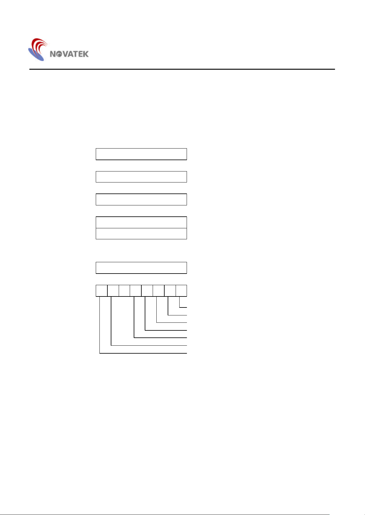
1. 6502 CPU
The 6502 is an 8-bit CPU that provides 56 instructions, decimal and binary arithmetic, thirteen addressing modes, true indexing
capability, programmable stack pointer with variable length stack, a wide selection of addressable memory, and interrupt input
options.
The CPU clock cycle is 4MHz (8MHz system clock divided by 2). Refer to 6502 data sheet for more details.
07
Accumulator A
7
Index Register Y
7 0
Index Register X
Program Counter PCH
PCL
7 0
7
Stack Pointer SP
N Status Register P
V B D I Z
0
815
0
07
C
Carry
Zero
IRQ Disable
Decimal Mode
BRK Command
Overflow
Negative
1 = TRUE
1 = Result ZERO
1 = DISABLE
1 = TRUE
1 = BRK
1 = TRUE
1 = NEG
Figure 1. 6502 CPU Registers and Status Flags
5
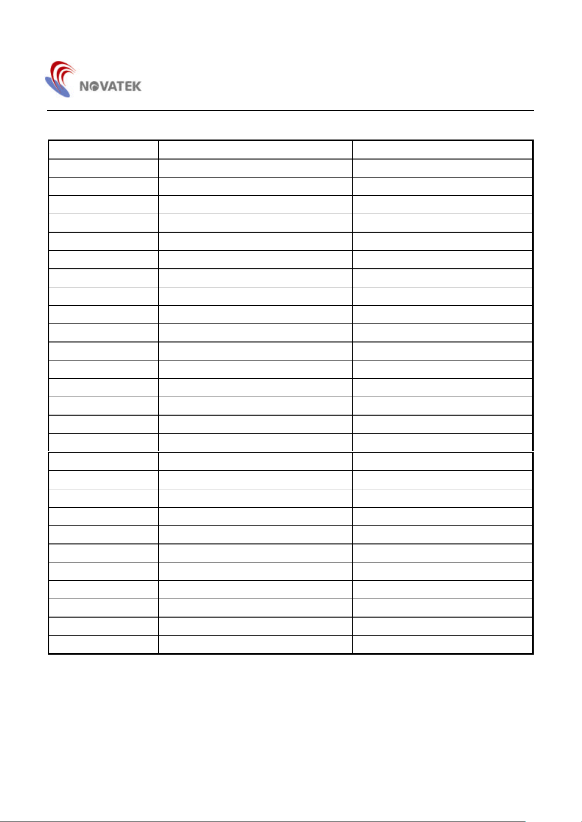
2. Instruction set list
Instruction Code Meaning Operation
ADC Add with carry A + M + C → A, C
AND Logical AND A • M → A
ASL Shift left one bit C ← M7 • • • M0 ← 0
BCC Branch if carry clears Branch on C = 0
BCS Branch if carry sets Branch on C = 1
BEQ Branch if equal to zero Branch on Z = 1
BIT Bit test A • M, M7 → N, M6 → V
BMI Branch if minus Branch on N = 1
BNE Branch if not equal to zero Branch on Z = 0
BPL Branch if plus Branch on N = 0
BRK Break Forced Interrupt PC+2 ↓ PC ↓
BVC Branch if overflow clears Branch on V = 0
NT6861
BVS Branch if overflow sets Branch on V = 1
CLC Clear carry 0 → C
CLD Clear decimal mode 0 → D
CLI Clear interrupt disable bit 0 → I
CLV Clear overflow 0 → V
CMP Compare accumulator to memory A − M
CPX Compare with index register X X − M
CPY Compare with index register Y Y − M
DEC Decrement memory by one M − 1 → M
DEX Decrement index X by one X − 1 → X
DEY Decrement index Y by one Y − 1→ Y
EOR Logical exclusive-OR A ⊕ M → A
INC Increment memory by one M + 1 → M
INX Increment index X by one X + 1 → X
INY Increment index Y by one Y + 1 → Y
6
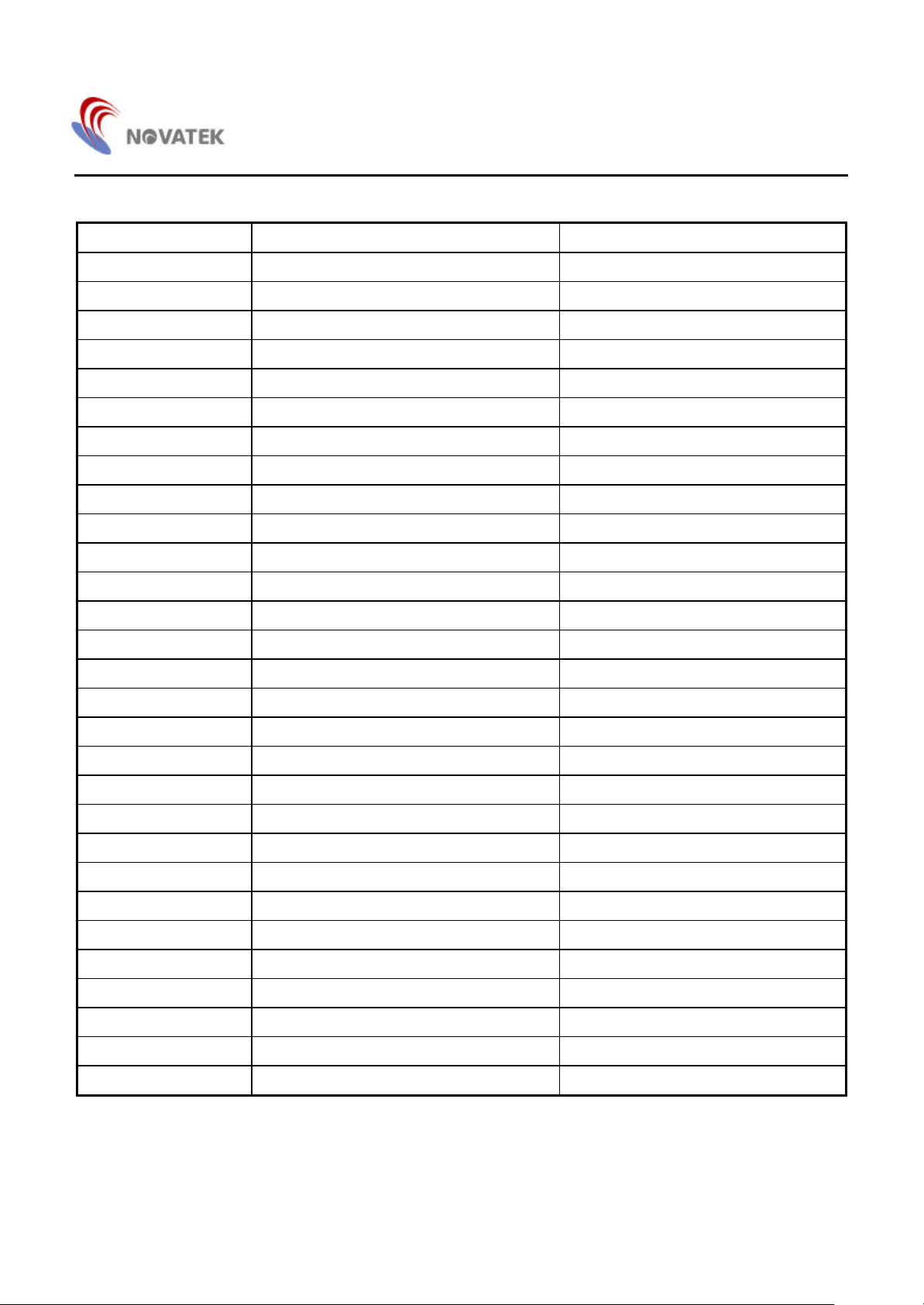
Instruction set list (continued)
Instruction Code Meaning Operation
JMP Jump to new location (PC+1) → PCL, (PC+2) → PCH
JSR Jump to subroutine PC + 2 ↓, (P+1) → PCL, (PC+2) → PCH
LDA Load accumulator with memory M → A
LDX Load Index register X with memory M → X
LDY Load Index register Y with memory M → Y
LSR Shift right one bit 0 → M7 • • • M0 → C
NOP No operation No operation (2 cycles)
ORA Logical OR A + M → A
PHA Push accumulator on stack A ↓
PHP Push status register on stack P ↓
PLA Pull accumulator from stack A ↑
PLP Pull status register from stack P ↑
NT6861
ROL Rotate left through carry C ← M7 • • • M0 ← C
ROR Rotate right through carry C → M7 • • • M0 → C
RTI Return from interrupt P ↑, PC ↑
RTS Return from subroutine PC ↑, PC+1 → PC
SBC Subtract with borrow A − M − C → A, C
SEC Set carry 1 → C
SED Set decimal mode 1 → D
SEI Set interrupt disable status
STA Store accumulator in memory A → M
STX Store index register X in memory X → M
STY Store index register Y in memory Y → M
TAX Transfer accumulator to index X A → X
TAY Transfer accumulator to index Y A → Y
TSX Transfer stack pointer to index X S → X
TXA Transfer index X to accumulator X → A
TXS Transfer index X to stack Pointer X → S
1 → I
TYA Transfer index Y to accumulator Y → A
* Refer to 6502 programming data book for more details.
7
NT6861
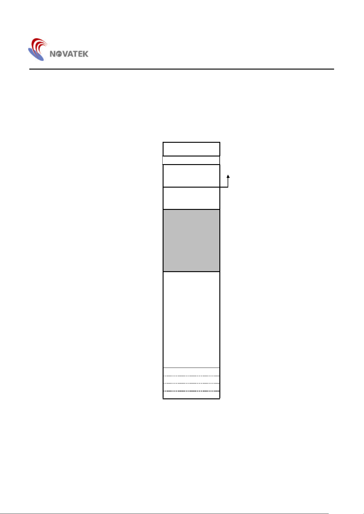
3. RAM: 256 X 8 bits
256 X 8-bit SRAM is used for data memory and stack. The RAM addressing range is from $0080 to $017F. From $0100 to
$017F is used as the EDID data buffer when activating DDC1/2B mode transmission. The contents of RAM are undetermined
at power-up and are not affected by system reset. Software programmers can allocate stack area in the RAM by setting stack
pointer register S. Because the 6502 default stack pointer is $01FF, programmers must set register S to FFH when starting the
program, so the stack area will map $01FF - $0180 to $00FF - $0080.
as; LDX #$FF
TXS
$0000
$0025
$0080
$00FF
$0100
$017F
$0180
System Registers
Unused
RAM
stack pointer
EDID
$BFFF
$A000
(4/8/12/16/24K Bytes)
$FFFC RST-L
$FFFD
$FFFE
$FFFF
Unused
ROM
RST-H
IRQ-L
IRQ-H
RESET vector
IRQ vector
8
NT6861
HPOLO
VPOLO
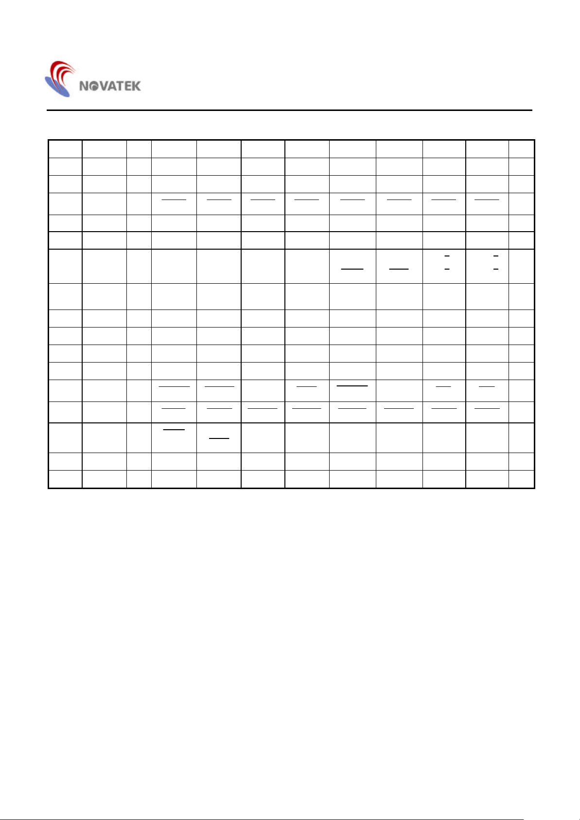
4. System Registers
Addr. Register INIT Bit7 Bit6 Bit5 Bit4 Bit3 Bit2 Bit1 Bit0
$0000 PT0 FFH P07 P06 P05 P04 P03 P02 P01 P00 RW
$0001 PT1 7FH - P16 P15 P14 P13 P12 P11 P10 RW
$0002 PT2DIR FFH
$0003 PT2 FFH P27 P26 P25 P24 P23 P22 P21 P20 RW
$0004 PT3 03H - - - - - - P31 P30 RW
$0005 MD CON 07H
$0006 HV CON 2FH HCNTOV VCNTOV HSYNCI VSYNCI HPOLI VPOLI
$0007 HCNT L 00H HCL7 HCL6 HCL5 HCL4 HCL3 HCL2 HCL1 HCL0 R
$0008 HCNT H 00H - - - - HCH3 HCH2 HCH1 HCH0 R
$0009 VCNT L 00H VCL7 VCL6 VCL5 VCL4 VCL3 VCL2 VCL1 VCL0 R
$000A VCNT H 00H - - - - VCH3 VCH2 VCH1 VCH0 R
$000B SYNCON FFH
$000C ENDAC FFH
$000D AD0 REG
$000E AD1 REG 00H - - AD15 AD14 AD13 AD12 AD11 AD10 R
$000F IEX 00H - - IEINTS IEINTD IEINTA IEINTR IEINTE IEINTV W
C0
P27OE P26OE P25OE P24OE P23OE P22OE P21OE P20OE
-
-
NOHALF ENHALF
ENAD1 ENAD0 ENDK13 ENDK12 ENDK11 ENDK10 ENDK9 ENDK8
CEND
H
-
-
CSTA
-
-
-
AD05 AD04 AD03 AD02 AD01 AD00
-
-
FRUN FRFREQ
-
INSEN
-
HSEL
HALFPOL
S/C
S/C
ENH ENV
MD1/ 2
MD1/ 2
W
W
W
W
W
W
R
R
R
9
NT6861
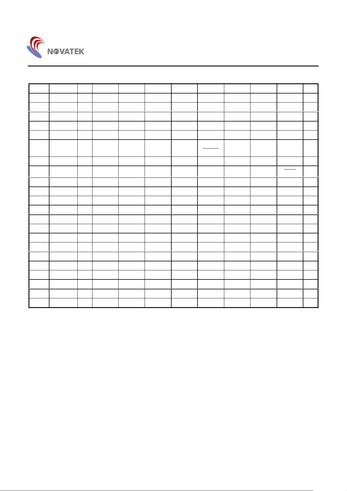
System Registers (continued)
Addr. Register INIT Bit7 Bit6 Bit5 Bit4 Bit3 Bit2 Bit1 Bit0
$0010 IRQX 00H - - IRQINTS IRQINTD IRQINTA IRQINTR IRQINTE IRQINTV R
$0011 CLR FLG 00H CLRHOV CLRVOV CLRINTS CLRINTD CLRINTA CLRINTR CLRINTE CLRINTV W
$0012 CLR WDT - 0 1 0 1 0 1 0 1 W
$0013 II ADR FFH AR7 AR6 AR5 AR4 AR3 AR2 AR1 - W
$0014 II DAT 00H SR7 SR6 SR5 SR4 SR3 SR2 SR1 SR0 RW
$0015 II STS 08H - - START
START
$0016 BT 00H BT7 BT6 BT5 BT4 BT3 BT2 BT1 BT0 W
STOP
STOP
ENDDC
TRX
RXAK - R
W
$0017 BT CON 03H - - - - - - TBS
$0018 DACH0 80H DKVL7 DKVL6 DKVL5 DKVL4 DKVL3 DKVL2 DKVL1 DKVL0 RW
$0019 DACH1 80H DKVL7 DKVL6 DKVL5 DKVL4 DKVL3 DKVL2 DKVL1 DKVL0 RW
$001A DACH2 80H DKVL7 DKVL6 DKVL5 DKVL4 DKVL3 DKVL2 DKVL1 DKVL0 RW
$001B DACH3 80H DKVL7 DKVL6 DKVL5 DKVL4 DKVL3 DKVL2 DKVL1 DKVL0 RW
$001C DACH4 80H DKVL7 DKVL6 DKVL5 DKVL4 DKVL3 DKVL2 DKVL1 DKVL0 RW
$001D DACH5 80H DKVL7 DKVL6 DKVL5 DKVL4 DKVL3 DKVL2 DKVL1 DKVL0 RW
$001E DACH6 80H DKVL7 DKVL6 DKVL5 DKVL4 DKVL3 DKVL2 DKVL1 DKVL0 RW
$001F DACH7 80H DKVL7 DKVL6 DKVL5 DKVL4 DKVL3 DKVL2 DKVL1 DKVL0 RW
$0020 DACH8 80H DKVL7 DKVL6 DKVL5 DKVL4 DKVL3 DKVL2 DKVL1 DKVL0 RW
$0021 DACH9 80H DKVL7 DKVL6 DKVL5 DKVL4 DKVL3 DKVL2 DKVL1 DKVL0 RW
$0022 DACH10 80H DKVL7 DKVL6 DKVL5 DKVL4 DKVL3 DKVL2 DKVL1 DKVL0 RW
$0023 DACH11 80H DKVL7 DKVL6 DKVL5 DKVL4 DKVL3 DKVL2 DKVL1 DKVL0 RW
$0024 DACH12 80H DKVL7 DKVL6 DKVL5 DKVL4 DKVL3 DKVL2 DKVL1 DKVL0 RW
$0025 DACH13 80H DKVL7 DKVL6 DKVL5 DKVL4 DKVL3 DKVL2 DKVL1 DKVL0 RW
ENBT
Note:The line above a writable signal name indicate an active low signal
The dash line in these control register indicate an undefined bit
The address of control register from $0026 to $007F are not used.
W
10
NT6861
5. Timing Generator
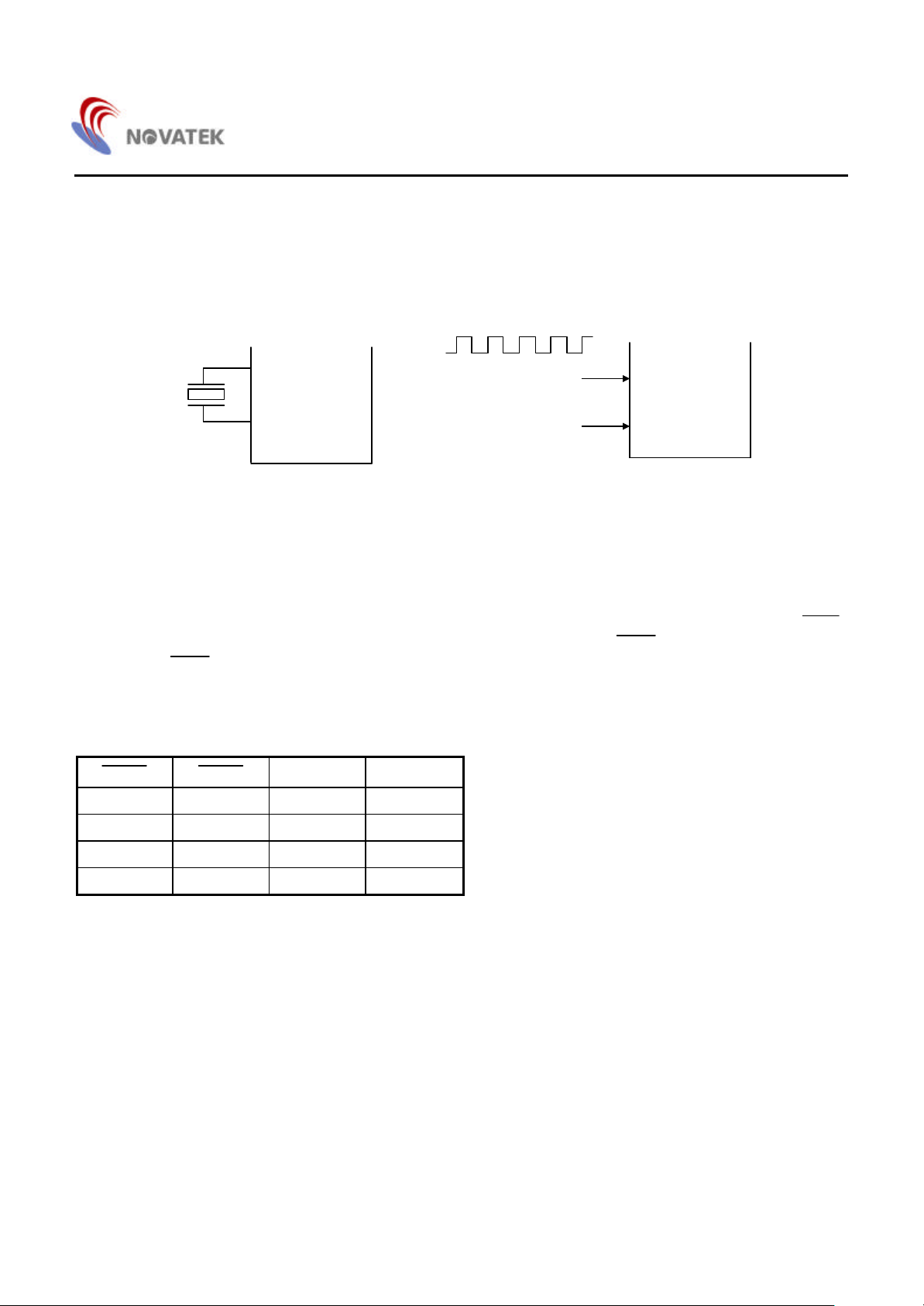
This block generates the system timing and control signal to be supplied to the CPU and on-chip peripherals. A crystal quartz,
ceramic resonator, or an external clock signal provided to the OSCI pin generates 8MHz system clock,
(4 MHz for CPU), Although internal circuits have a feedback resistor and compacitor included, components may be externally
added to ensure proper operation. The typical clock frequency is 8MHz. This frequency will affect the operation of on-chip
peripherals whose operating frequency is based on the system clock .
OSCI
8MHz
OSCO
(1)
NT6861
External Clock
Unconnected
OSCI
OSCO
(2)
NT6861
Figure 2. Oscillator Connections
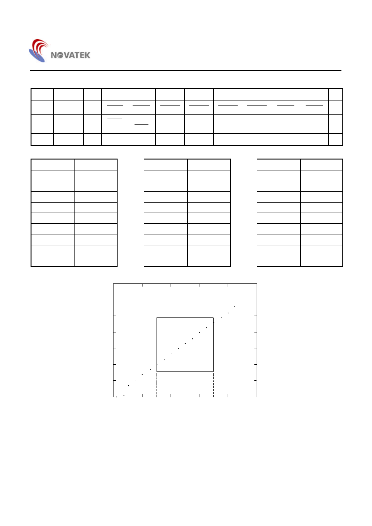
6. A/D Converter
The analog to digital converter is a single 6-bit successive approximation converter. Analog voltage is supplied from external
sources to the A/D input pins and the results of the conversion are stored in the 6-bit data latch registers
($000D & $000E). The A/D converter is controlled by the control bits in the A/D control register ENDAC. Refer to the A/D
channel format table A/D input pins activation. A conversion is started by setting a '0' to the CONVERSION START bit ( CSTA)
in the A/D control register ($000D). This automatically sets the CONVERSION END bit ( CEND ) to '1'. When a conversion has
been finished, CEND bit automatically clears to '0'. The A/D conversion data in the AD LATCH registers ($000D & $000E) is
valid digital data.
The analog voltage to be measured should be stabled during the conversion operation. The variation should exceed
1/2 LSB for accuracy in measurement. Please refer Figure 3 for checking the linearity of A/D.
A/D Channel Format Table
ENAD1 ENAD0
0 0 AD1 AD0
P11 line P10 line
0 1 AD1 P10
1 0 P11 AD0
1 1 P11 P10
11
NT6861
A/D Channel Control Register
Addr. Register INIT Bit7 Bit6 Bit5 Bit4 Bit3 Bit2 Bit1 Bit0
$000C ENDAC FFH
$000D AD0 REG C0H
$000E AD1 REG 00H - - AD15 AD14 AD13 AD12 AD11 AD10 R
ENAD1 ENAD0 ENDK13 ENDK12 ENDK11 ENDK10 ENDK9 ENDK8
CEND
CSTA
AD05 AD04 AD03 AD02 AD01 AD00
Input Voltage Digital Value Input Voltage Digital Value Input Voltage Digital Value
1.5 19 ($13) 2.22 28 ($1C) 2.91 37 ($25)
1.58 20 ($14) 2.29 29 ($1D) 2.98 38 ($26)
1.65 21($15) 2.37 30 ($1E) 3.06 39 ($27)
1.73 22 ($16) 2.45 31 ($1F) 3.15 40 ($28)
1.81 23 ($17) 2.53 32 ($20) 3.24 41 ($29)
1.90 24 ($18) 2.61 33 ($21) 3.32 42 ($2A)
1.97 25 ($19) 2.68 34 ($22) 3.40 43 ($2B)
2.06 26 ($1A) 2.76 35 ($23) 3.47 44 ($2C)
2.14 27 ($1B) 2.84 36 ($24) 3.55 45 ($2D)
70
These digitals have 1 LSB deviation
60
±
W
R
W
50
40
Digital Value
30
20
10
0
0
Linear Range
0.4 0.6 0.8 1
0.3 0.7
0.2
Input Voltage
Figure 3. A/D Converter Linearity Diagram
12
VDD
NT6861
7. PWM DACs (Pulse Width Modulation D/A Converters)
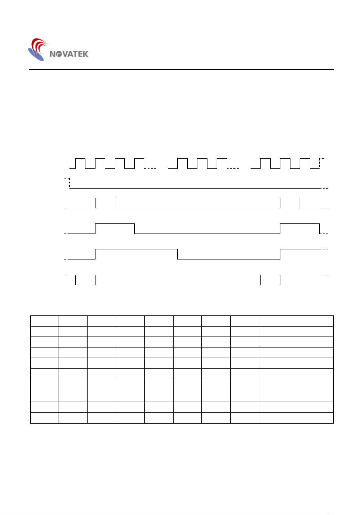
There are 14 PWM D/A converters with 8-bit resolution in NT6861. Eight of these D/A (DAC0 - DAC7) converters are opendrain output structures with 12V applied (maximum), and the other six D/A converters (DAC8 - DAC13) are
open-drain output structures with 5V applied (maximum). The PWM frequency is 31.25 KHz on 8 MHz system clock. Use of a
different oscillator frequency will result in different PWM frequency. As DAC8 - DAC13 are shared with I/O port pins, user can
write '0' to corresponding enable bit in the ENDAC control register to activate each of DACH8 - 13. There are 14-channel
readable DACH registers corresponding to 14 D/A converters. Each PWM output pulse width is programmable by setting the 8
bit digital to the corresponding DACH registers. When these DACH registers are set to 00H, the DAC will output LOW (GND
level) and each bit addition will add 125ns pulse width. After reset, all DAC outputs are set to 80H (1/2 duty output ). Refer to
Figure 4 for the detailed timing diagram of PWM D/A output.
8MHz Fosc
PWM value:
255 (FF)
255 0 1 2 m m+1 m+2 255 0 1
00
01
02
m
Figure 4. The DAC Output Timing Diagram and Wave Table
DKVL7 DKVL6 DKVL5 DKVL4 DKVL3 DKVL2 DKVL1 DKVL0 DAC Output Duty Cycle
0 0 0 0 0 0 0 0 GND
0 0 0 0 0 0 0 1 1/256 Vref.
0 0 0 0 0 0 1 0 2/256 Vref.
0 0 0 0 0 0 1 1 3/256 Vref.
0 0 0 0 0 1 0 0 4/256 Vref.
-
-
-
-
-
-
-
-
-
-
-
-
-
-
-
-
-
-
-
-
-
-
-
X /256 Vref.
1 1 1 1 1 1 1 0 254/256 Vref.
1 1 1 1 1 1 1 1 255/256 Vref.
The DAC value correspondent to PWM Output * Vref. is 12V or 5V
13
NT6861
Addr. Register INIT Bit7 Bit6 Bit5 Bit4 Bit3 Bit2 Bit1 Bit0
$000C ENDAC FFH
$0018 DACH0 80H DKVL7 DKVL6 DKVL5 DKVL4 DKVL3 DKVL2 DKVL1 DKVL0 RW
$0019 DACH1 80H DKVL7 DKVL6 DKVL5 DKVL4 DKVL3 DKVL2 DKVL1 DKVL0 RW
$001A DACH2 80H DKVL7 DKVL6 DKVL5 DKVL4 DKVL3 DKVL2 DKVL1 DKVL0 RW
$001B DACH3 80H DKVL7 DKVL6 DKVL5 DKVL4 DKVL3 DKVL2 DKVL1 DKVL0 RW
$001C DACH4 80H DKVL7 DKVL6 DKVL5 DKVL4 DKVL3 DKVL2 DKVL1 DKVL0 RW
$001D DACH5 80H DKVL7 DKVL6 DKVL5 DKVL4 DKVL3 DKVL2 DKVL1 DKVL0 RW
$001E DACH6 80H DKVL7 DKVL6 DKVL5 DKVL4 DKVL3 DKVL2 DKVL1 DKVL0 RW
$001F DACH7 80H DKVL7 DKVL6 DKVL5 DKVL4 DKVL3 DKVL2 DKVL1 DKVL0 RW
$0020 DACH8 80H DKVL7 DKVL6 DKVL5 DKVL4 DKVL3 DKVL2 DKVL1 DKVL0 RW
$0021 DACH9 80H DKVL7 DKVL6 DKVL5 DKVL4 DKVL3 DKVL2 DKVL1 DKVL0 RW
$0022 DACH10 80H DKVL7 DKVL6 DKVL5 DKVL4 DKVL3 DKVL2 DKVL1 DKVL0 RW
$0023 DACH11 80H DKVL7 DKVL6 DKVL5 DKVL4 DKVL3 DKVL2 DKVL1 DKVL0 RW
$0024 DACH12 80H DKVL7 DKVL6 DKVL5 DKVL4 DKVL3 DKVL2 DKVL1 DKVL0 RW
$0025 DACH13 80H DKVL7 DKVL6 DKVL5 DKVL4 DKVL3 DKVL2 DKVL1 DKVL0 RW
ENAD1 ENAD0 ENDK13 ENDK12 ENDK11 ENDK10 ENDK9 ENDK8
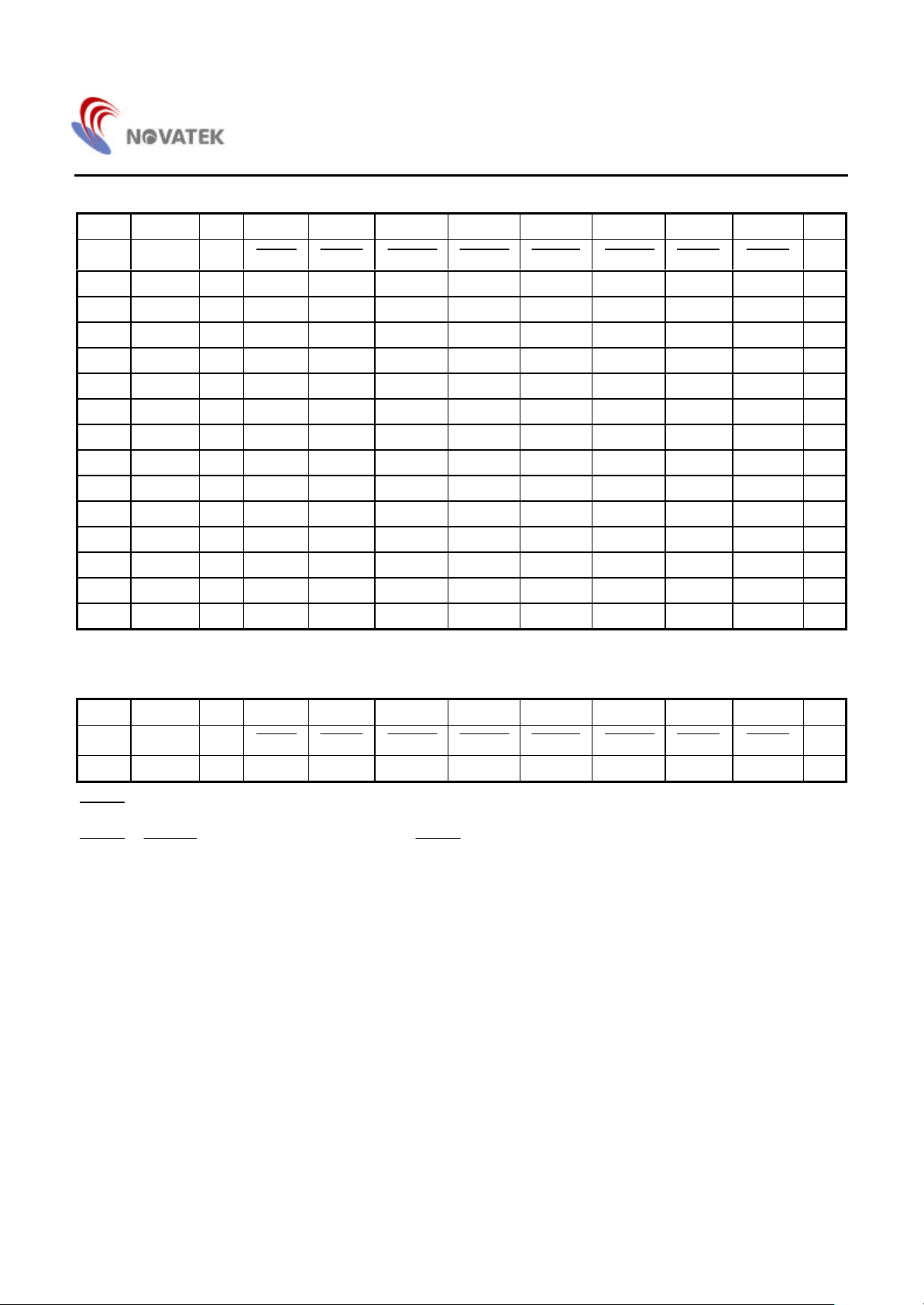
DAC control register ($000C) and DAC value register ($0018 - $0025)
Control Bit Description:
W
Addr. Register INIT Bit7 Bit6 Bit5 Bit4 Bit3 Bit2 Bit1 Bit0
$000C ENDAC FFH
$0018 DACH0 80H DKVL7 DKVL6 DKVL5 DKVL4 DKVL3 DKVL2 DKVL1 DKVL0 RW
ENAD1 ENAD0 ENDK13 ENDK12 ENDK11 ENDK10 ENDK9 ENDK8
W
ENDK8:Enable DAC channel 8; When clearing this bit to '0', the I/O port, P00, will change to DAC channel 8.
When setting this bit to '1', the I/O port will restore to P00.
ENDK9 - ENDK13: The manipulation is the same as ENDK8 bit, and control DAC channel 9 - 13.
DACH0 (DKVL0 - DKVL7): Setting DAC output waveform of DAC channel 8. Please check Figure 3 for the timing diagram
and wave table.
DACH1 - DACH13: The manipulation is the same as DACH0 register, and control DAC channel 1 - 13.
14
 Loading...