NOVATEK NT6828, NT6828K Datasheet
Features
I2C Bus Interface with Slave Address $7A (Receiver
Only)
Horizontal Frequency Range: 30KHz ~ 120KHz
Flexible Display Resolution: up to 1524 dots per row
Internal PLL Generating a Stable and Wide-Ranged
System Clock (92.2 MHz)
OSD Screen Comprising of Character Arrays of 15
Rows by 30 Columns
12 X 18 Dot Matrix Per Character
Total of 256 Fonts Including 248 ROM Fonts and 8
RAM Fonts
Programmable Vertical and Horizontal Position
Adjustment for OSD Display Position
General Descriptio n
NT6828 is designed for displaying symbols and
characters onto a CRT monitor. Its operation is controlled
by the micro-controller with I2C bus interface. By sending
the proper data and commands to NT6828, it can carry
out the full screen display automatically while the time
base is generated by the on-chip PLL circuit. There are
many functions provided on this chip to fully support
numerous user applications. These functions are:
adjustment of OSD windows position, built-in ROM &
NT6828
I2C Bus Controlled On-Screen Display
8-Color Selection for Each Character and 8-Color
Control on Each Row with Overlapped by Windows
Character Blinking, Shadowing & Bordering Display
Effects
Double Character Height and Width for Each Row
Program mable Hei ght of Charact ers Displ ay
Row To Row Spacing Control
Four Overlapping and Programmable Windows with 8-
Color Control
Hsync & Vsync Input Polarity Selectable
8 Channels PWM DAC with 8 bits resolution & Open-
Drain Output Structure
16 DIP and 24 Skinny DIP packages
RAM fonts, variable character height with row-to-row
spacing adjustment, 8 color selections for each character,
double height/width controls for each row, four available
overlapping windows with color & size controls, as well as
other I/O interfaces to compliment an external video
chipset.
NT6828 provides eight optional PWM channels with 8-bit
resolution for external digital to analog control.
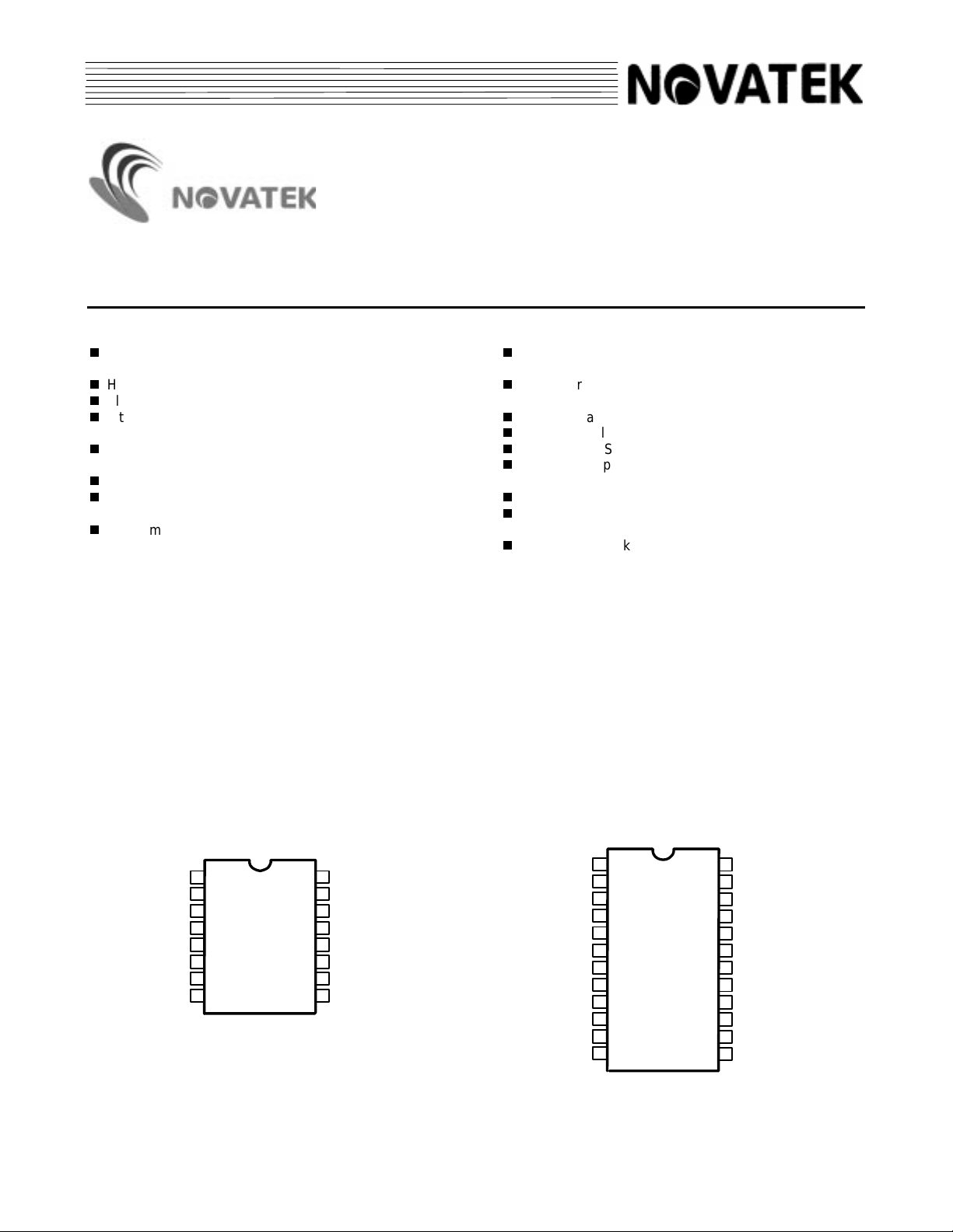
Pin Configurations
AGND
VCO
AVCC
HFLB
N.C.
SDA
SCL DVCC
RP
1
2
3
4
5
6
7
8
16 DIP
16
15
NT6828
14
13
12
11
10
DGND
R
G
B
FBKG
PWM/HFTON
VFLB
9
24 Skinny DIP
AGND
VCO
RP
AV
DD
HFLB
N.C.
SDA
SCL
PWM0
PWM1
PWM2
PWM3
1
2
3
4
5
6
7
8
9
10
11
12
24
23
22
21
NT6828K
20
19
18
17
16
15
14
13
DGND
R
G
B
FBKG
PWM/HFTON
VFLB
DVCC
PWM7
PWM6
PWM5
PWM4
1V2.1
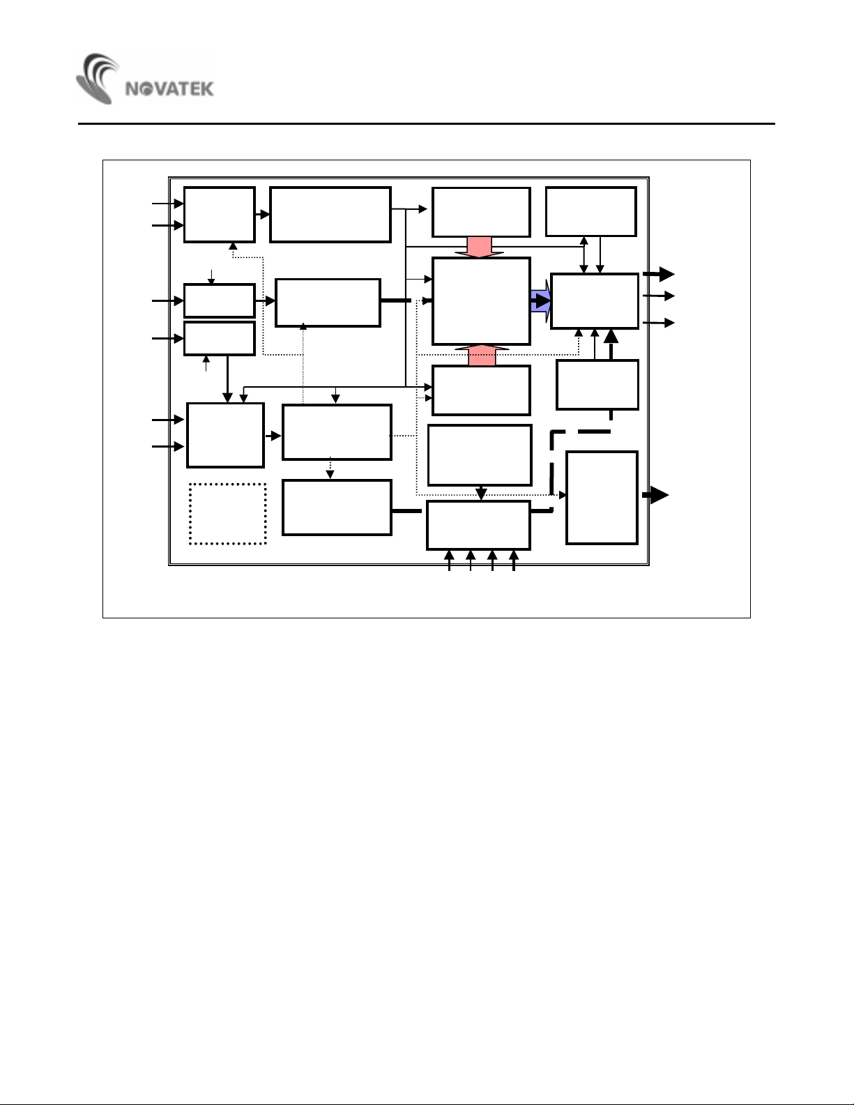
Block Diagram
NT6828
SCL
SDA
VFLB
HFLB
RP
VCO
I2C
BUS
RECEIVER
VPOL
VSYNC
HSYNC
HPOL
PLL
CIRCUIT
TEST
CIRCUIT
BUS CO NTRO L
BUFFER
VERTICAL
CONTROL
TIMING
GENERATOR
HORIZONTAL
CONTROL
ROM/RAM
FONT 12 * 18
DISPLAY
MEMORY
CONTOL
REG.
POWER ON
LOW VOLTAGE
RESET
POWER
SYSTEM
DISPLAY
EFFECT
OUTPUT
CONTROL
COL OR
CONT R OL
PWM
Channel
R/G/B
FBKG
PWM /
HFTON
PWM0-7
AVCC
DVCC
AGND
DGND
2
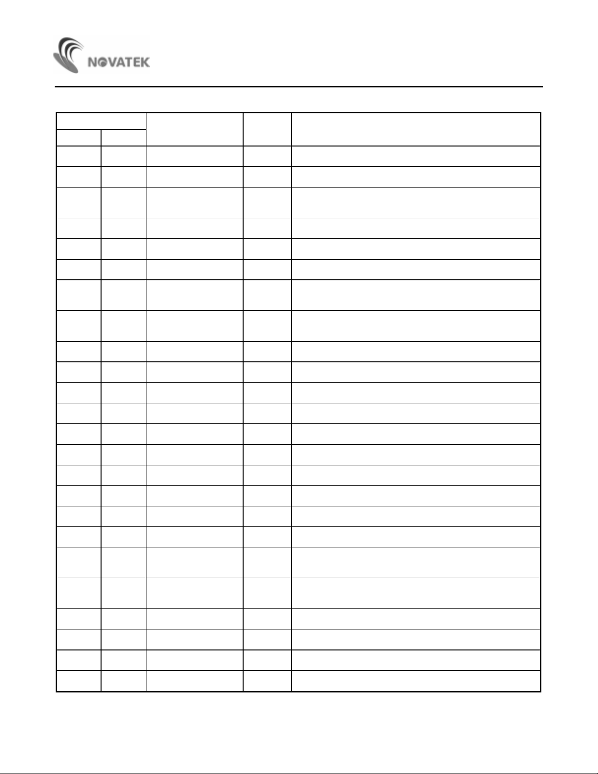
Pin Description
NT6828
Pin No.
16 Pin 24 Pin
1 1 AGND P Analog Ground
2 2 VCO - Voltage I/P to Control Oscillator
3 3 RP - Bias Resistor. (To be used as a bias internal VCO to
4 4 AVCC P Analog Power Supply (5V Typ.)
5 5 HFLB I Horizontal Fly-back Input (Schmitt Trigger Buffer)
6 6 N.C. - 7 7 SDA I SDA Pin Of I2C Bus (Schmitt Trigger Buffer) with internal
8 8 SCL I SCL Pin Of I2C Bus (Schmitt Trigger Buffer) with internal
9 PWM0 O 5V PWM Channel 0. Open-drain output structure
10 PWM1 O 5V PWM Channel 1. Open-drain output structure
11 PWM2 O 5V PWM Channel 2. Open-drain output structure
Designation I/O/P/R Description
resonate at the specific range of pixel clock)
100K ohm pulled-high resistance
100K ohm pulled-high resistance
12 PWM3 O 5V PWM Channel 3. Open-drain output structure
12 PWM4 O 5V PWM Channel 4. Open-drain output structure
14 PWM5 O 5V PWM Channel 5. Open-drain output structure
15 PWM6 O 5V PWM Channel 6. Open-drain output structure
16 PWM7 O 5V PWM Channel 7. Open-drain output structure
9 17 DVCC P Digital Power Supply (5V Typ.)
10 18 VFLB I Vertical Fly-back Input (Schmitt Trigger Buffer)
11 19 PWM/
HFTON
12 20 FBKG O Fast Blanking Output. (To be used as switching signal for the
13 21 B O Blue Color Output with Push-Pull Output Structure
14 22 G O Green Color Output with Push-Pull Output Structure
15 23 R O Red Color Output with Push-Pull Output Structure
16 24 DGND P D igital Ground
O PWM output or gain controlled of R,G,B channels.
R,G,B OSD video signals.)
3
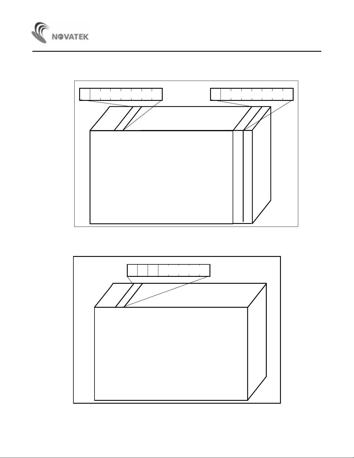
Functional Description
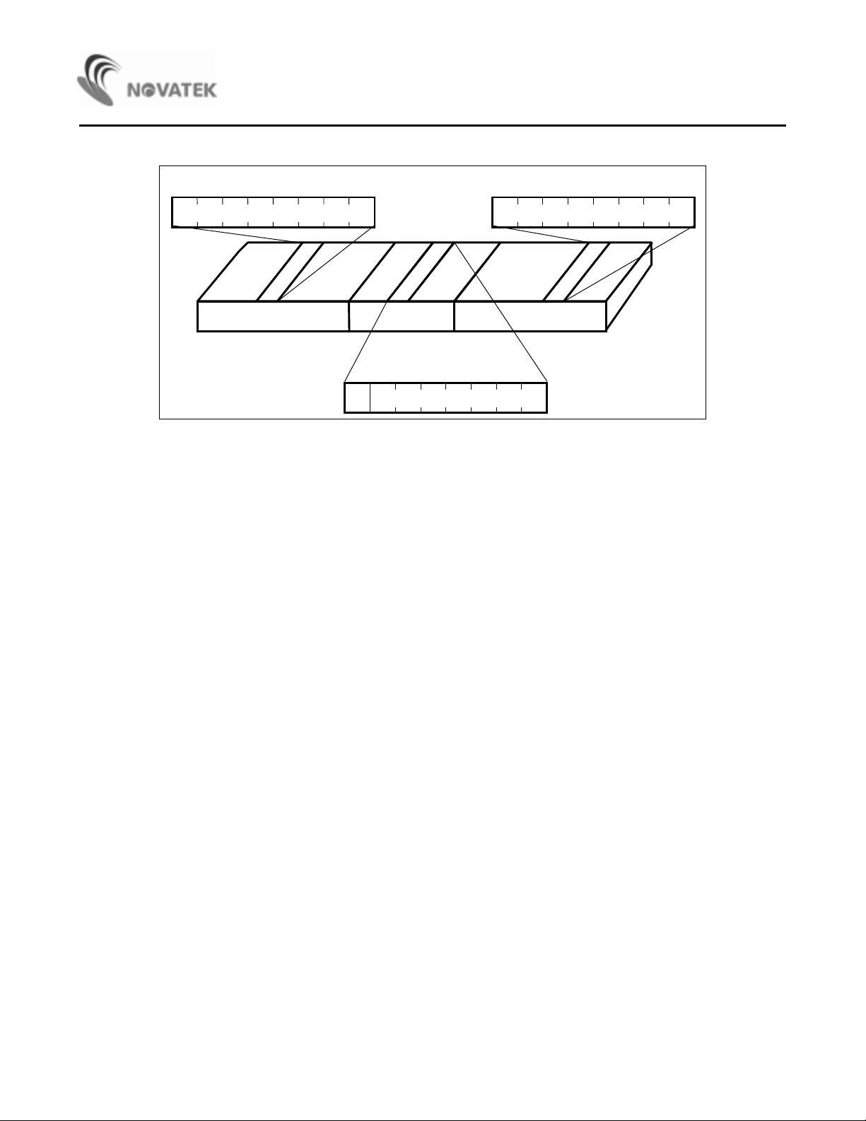
1. Memory Map
NT6828
07 07
Fonts Address $00-$ FF
00
ROW
14
Row Attri b ut e Reg ister
7
0
COLUMN
DISPLAY REGISTER
Memory Map of Display Register (Row 0 - 14)
07
Character Attribute
Register
29
30
7
0
31
RESERVED
ROW AT TRIBUTE REGISTER
7
0
0
029
ROW
14
CHARACTER ATTRIBUTE REGISTER
COLUMN
Memory Map of Attribute Register (Row 0 - 14)
4
NT6828
Window 1-4 Control Register
ROW
15
WINDOW1 - WINDOW4
0
07
7
0
OSD SCREEN
11
12 18
7
0
CONTROL
COLUMN
OSD Screen Control Register
Memory Map of Control Register (Row 15)
07
PWM Control Register
7
0
PWM CONTROL
2619
07
5
2. List of Control Regi st ers:
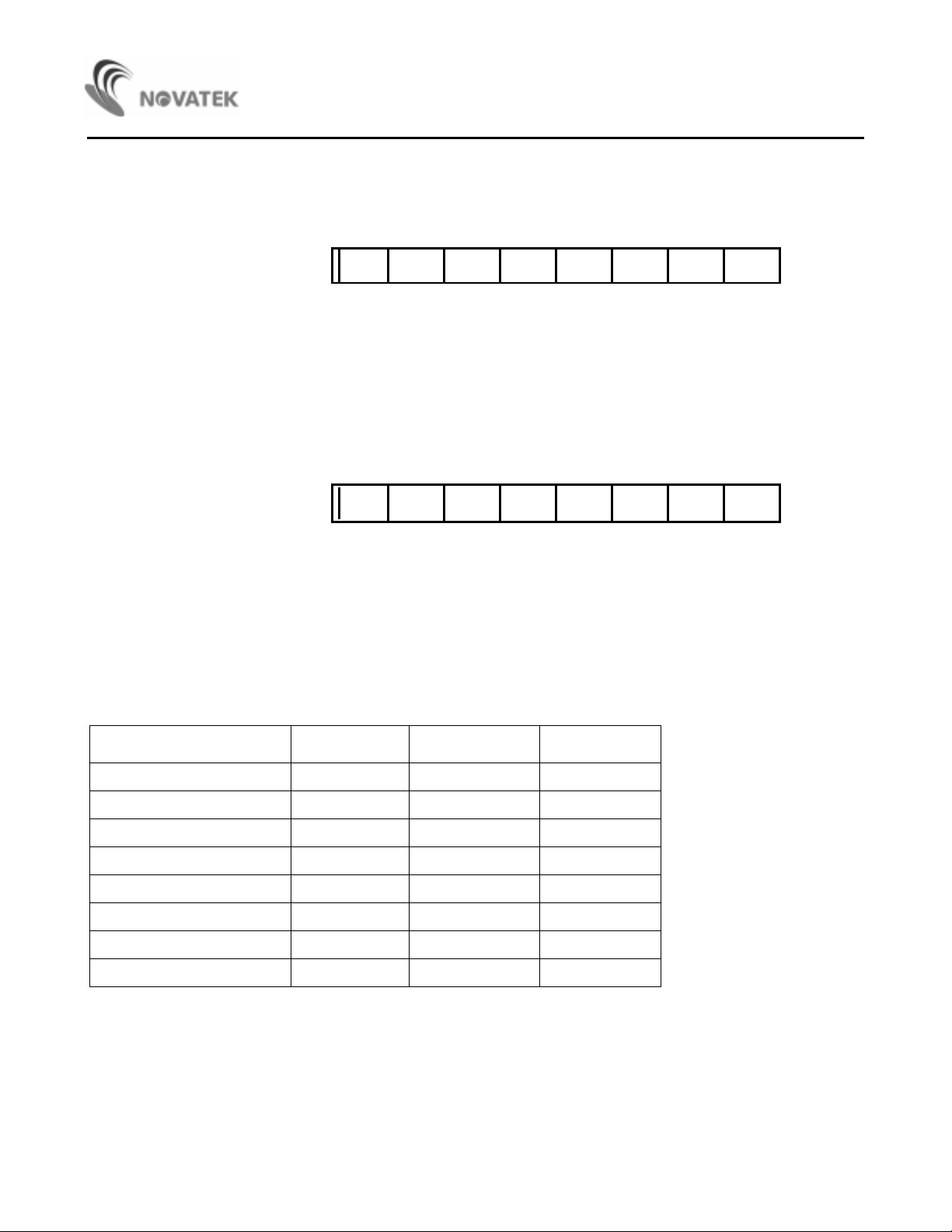
(1) Display Regis ter: Row 0 - 14, Column 0 - 29
76543210
Row 0-14
Column 0-29
MSB LSB
NT6828
Fonts’ Address $00 - $FF
Bit 7 - 0:
(2) Character Attribute Register: Row 0 - 14, Column 0 - 29
Bit 3: BLNK
Bit 2 - 0: R/G/B
Table 1. Character/Windows Color Selection
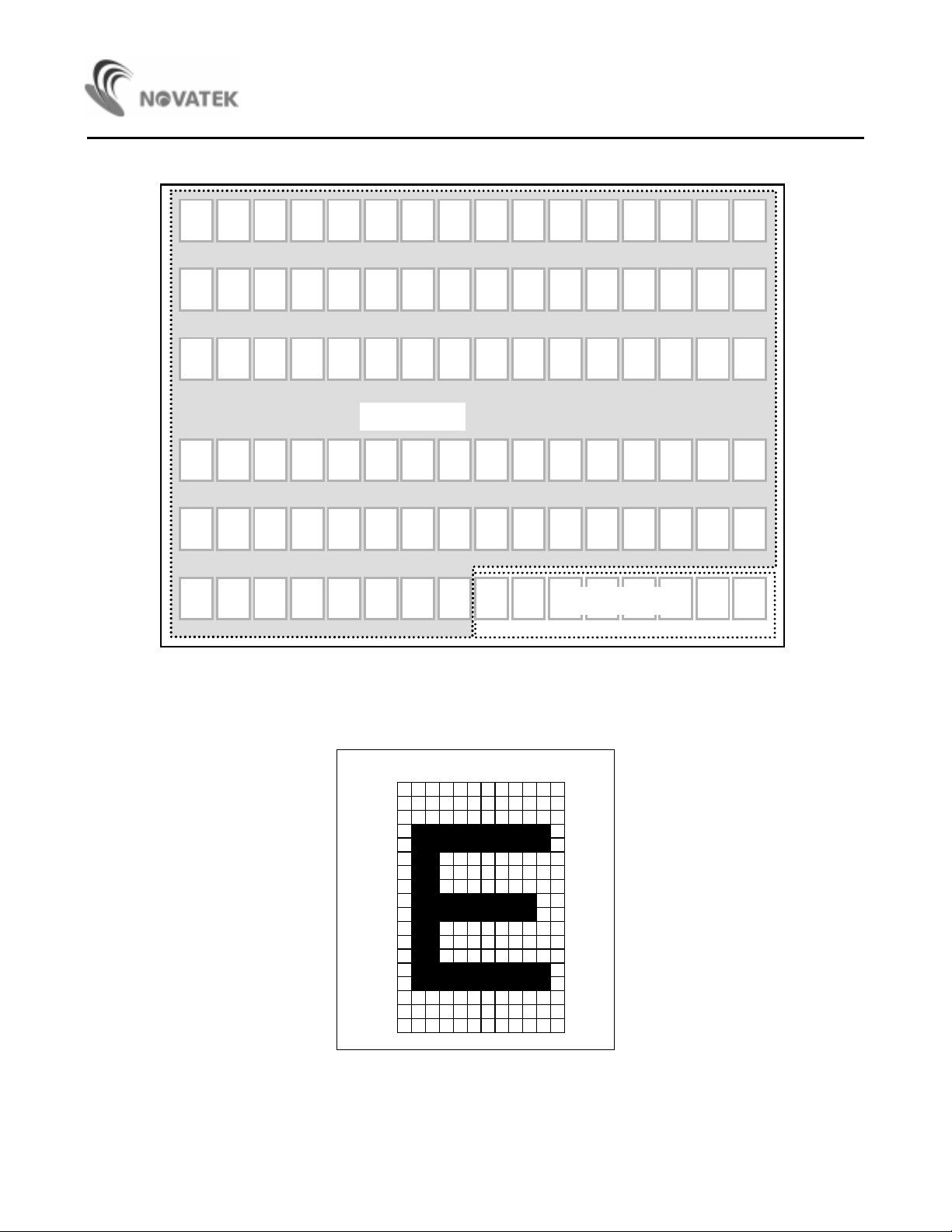
In this eight bit address one of the 256 characters/symbols resided in the character ROM/RAM fonts. (Please
refer to Figure 1.) Note that for 0 - 247 (ROM fonts) and 248 - 255 (RAM fonts) need to be programmed by the
user. Each font consists of 12 x 18 dots matrix. (Please refer to Figure 2.)
76543210
Row 0-14
Column 0-29
Characters’ Attribute Control
- This bit is to enable the blinking effect of the corresponding character/symbol as the bit is set to ‘1’. The
blinking frequency is approximately 1Hz with 50/50 duty cycle at 80Hz vertical sync frequency.
-These three bits define the color attributes of the corresponding character/symbol. (Please refer to Table
1 for the color selections.)
COLOR R G B
Black 0 0 0
BLNK R G B
Blue 0 0 1
Green 0 1 0
Cyan 0 1 1
Red 1 0 0
Magenta 1 0 1
Yellow 1 1 0
White 1 1 1
6
( 00 ) ( 01 ) ( 02 ) ( 03 ) ( 04 ) ( 05 ) ( 06 ) ( 07 ) ( 08 ) ( 09 ) ( 0A ) ( 0B ) ( 0C ) ( 0D ) ( 0E ) ( 0F )
(10 ) ( 11 ) ( 12 ) ( 13 ) ( 14 ) ( 15 ) ( 16 ) ( 17 ) ( 18 ) ( 19 ) ( 1A ) ( 1B ) ( 1C ) ( 1D ) ( 1E ) ( 1F )
NT6828
( 20 ) ( 21 ) ( 22 ) ( 23 ) ( 24 ) ( 25 ) ( 26 ) ( 27 ) ( 28 ) ( 29 ) ( 2A ) ( 2B ) ( 2C ) ( 2D ) ( 2E )
( 2F )
.
ROM Fonts
.
.
( D0 ) ( D1 ) ( D2 ) ( D3 ) ( D4 ) ( D5 ) ( D6 ) ( D7 ) ( D8 ) ( D9 ) ( DA ) ( DB ) ( DC ) ( DD ) ( DE ) ( DF )
( E0 ) ( E1 ) ( E2 ) ( E3 ) ( E4 ) ( E5 ) ( E6 ) ( E7 ) ( E8 ) ( E9 ) ( EA ) ( EB ) ( EC ) ( ED ) ( EE ) ( EF )
RAM Fonts
( F0 ) ( F1 ) ( F2 ) ( F3 ) ( F4 ) ( F5 ) ( F6 ) ( F7 ) ( F8 ) ( F9 ) ( FA ) ( FB ) ( FC ) ( FD ) ( FE ) ( FF )
Figure 1. Font Configuration
123456789101112
1
2
3
4
5
6
7
8
9
10
11
12
13
14
15
16
17
18
Figure 2. 12 x 18 Dots Matrix Font
7
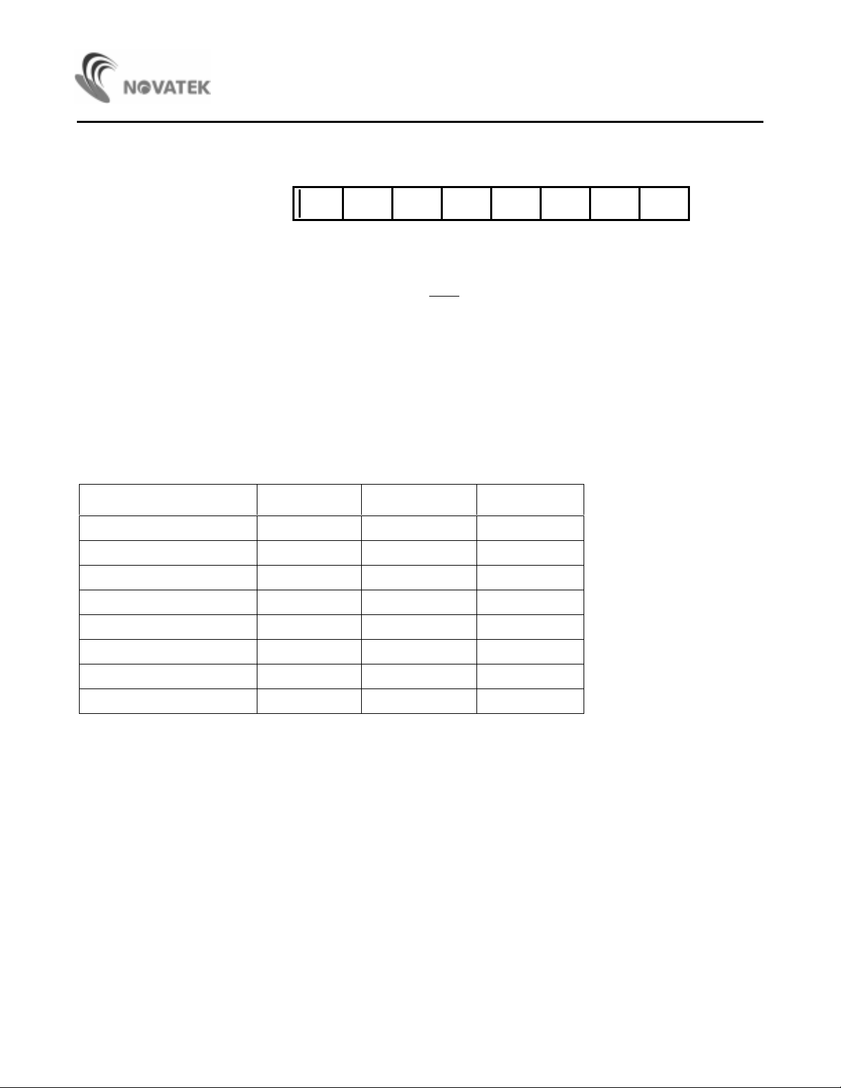
(3) Row At t ribute Register: R ow 0 - 14, Column 30
76543210
Row 0-14
Column 30
NT6828
RW GW BW DBH DBW
Bit 4 - 2: RW/GW/BW-
when overlapped by window and its control bit
selections.)
Bit 1: DBH
Bit 0: DBW
Table 2. Character/Windows Color Selection
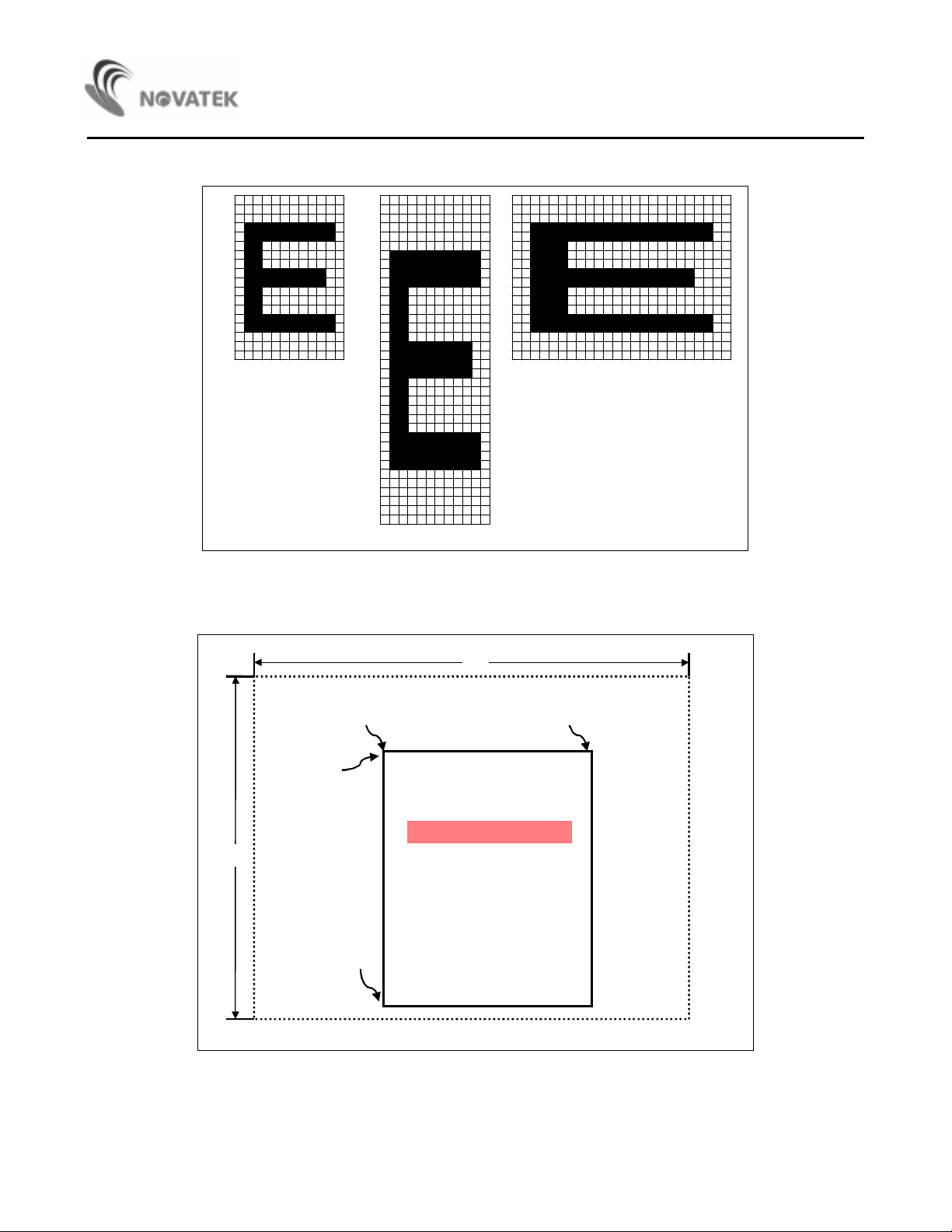
- This bit contr ols t he hei ght o f the d ispl ayed c hara cter /sym bol. When t his bi t is s et, th e cha ract er/s ymb ol is
displayed in double height. (Please refer to Figure 3.)
- Thi s bit contr ols the wid th of the di spla yed c hara cter/ symb ol. W hen thi s bit is set , th e ch aract er/ sym bol i s
displayed in double width. (Please refer to Figure 3.)
COLOR RW GW BW
Black 0 0 0
Blue 0 0 1
Green 0 1 0
Cyan 0 1 1
Red 1 0 0
These three bits define the color attributes of the corresponding character/symbol at each row
Rows’ Att
RO W cleared to ‘0’. (Pl ease refer to Tabl e 2 for the color
ribute Control
Magenta 1 0 1
Yellow 1 1 0
White 1 1 1
8
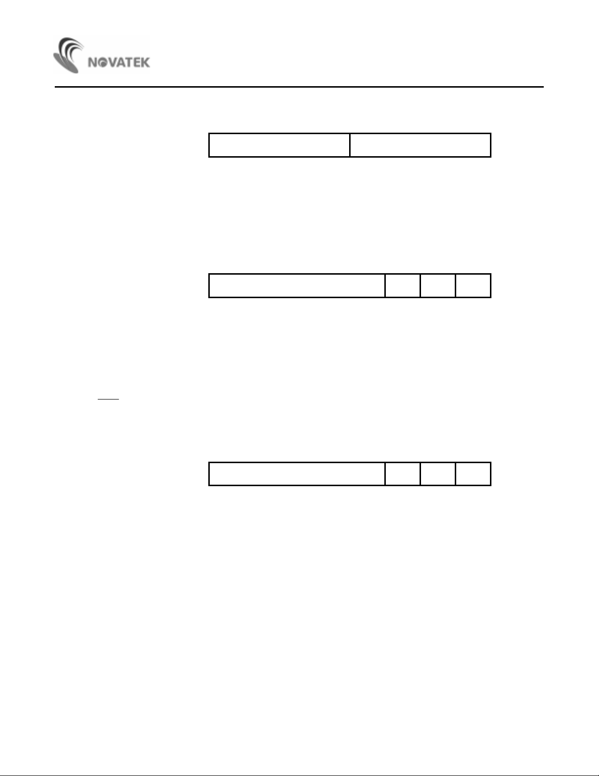
(4) Window 1 Registers: Row 15, Column 0
76543210
Row 15
Column 0
MSBLSBMSBLSB
NT6828
Row Start Address Row End Address
Window 1 Row Size Control
Bit 7 - 4:
Bit 3 - 0:
Bit 7 - 3:
Bit 2: WINEN
Bit 1:
These bits determine the row start position of window 1on the 15 x 30 OSD screen.
(Please refer to Figure 4.)
These bits determine the row end position of window 1on the 15 x 30 OSD screen.
(Please refer to Figure 4.)
76543210
Row 15
Column 1
These bits determine the column start position of window 1on the 15 x 30 OSD screen.
(Please refer to Figure 4.)
- This bit enables the window 1 as it is set.
ROW -
this bit to enable the row color attributes set by the control bit2~4 at the control registers at row 0 - 14, column 30.
This bit determines the row color attributes of the characters, which is overlapped by this window. Clear
Row 15
Column 2
MSB LSB
MSB LSB
Column Start Address
Window1 Column Size Control & Attribute Control
76543210
Column End Address
WINEN ROW_
RGB
Window1 Column Size Control & Attribute Control
Bit 7 - 3:
Bit 2 - 0: R/G/BNote:
Window 4 from 9 - 11. The function of Window 2 - 4 control registers is the same as Window 1. Window 1 has the
highest priority,
display area have overlapped. The higher priority color will take occupy the overlapping wi
These bits determine the column end position of window 1on the 15 x 30 OSD screen.
(Please refer to Figure 4.)
These bits control the background color of window 1. Please refer to the Table for color selection.
Window 1 control registers occupy column 0 - 2 of row 15, Window 2 from column 3 - 5, Window 3 from 6 - 8 and
whereas Window 4, the least whereas window with higher priority will overlap window with lower if their
ndow area.
If the start address of the row/column is greater than the end address then this window will not be
displayed.
Set out of 15 Row & 30 Column OSD display range , the abnormal OSD screen will be displayed.
9
NT6828
1234567 89101112
1
2
3
4
5
6
7
8
9
10
11
12
13
14
15
16
17
18
Normal
123456 789101112
1
2
3
4
5
6
7
8
9
10
11
12
13
14
15
16
17
18
19
20
21
22
23
24
25
26
27
28
29
30
31
32
33
34
35
36
1 2 3 4 5 6 7 8 9 10 11 12 13 14 15 16 17 18 19 20 21 22 23 24
1
2
3
4
5
6
7
8
9
10
11
12
13
14
15
16
17
18
Double Width
Double Height
Figure 3. Double Height & Width Effect
15
30
Column Start Address
Row Start Address
WINDOW1/2/3/4 AREA
Row Start/End Control Register:
row15 /column 0/3/6/9
Column Start Control Register:
row15 /column 1/4/7/10
Column End Control Register:
row15 /column 2/5/8/11
Window Color Control Register:
row15 /column 2/5/8/11
Row End Address
Figure 4. Windows’ Size Setting
Column End Address
10
 Loading...