NOVATEK NT3980 Datasheet

NT3980
TFT LCD Source Driver
Features
n Output: 384 output channels
n 8-bit resolution /256 gray scales
n Dot inversion with polarity control
n V1 ~ V10 for adjusting Gamma correction
n Power for analog circuit: 7 ~ 10V
n Output dynamic range: 0.1V ~ AV DD-0.1
n Power consumption of analog circuit: 6mA
General Description
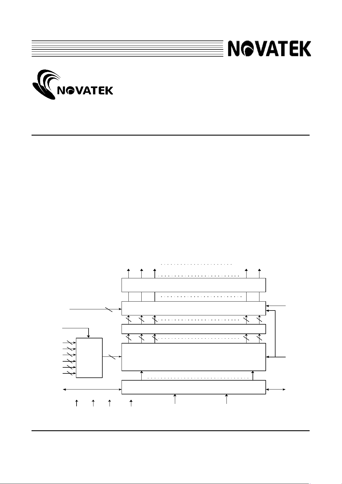
The NT3980 is a data driver IC for a color TFT LCD panel, XGA and SXGA applications. It receives 8 bit per-pixel digital display
data,and generates output voltage for 256 grayscales ,enabling a maximum of 16.77M display colors . For better performance,
dot inversion and a wide range voltage output, 10V, are designed in this chip, and for reducing EMI, data inversion control is
used. This chip supplies 10 sections of voltage-reference for Gamma correction.
n Operating frequency: 70MHz(Vcc:3.0V~3.6V)
45MHz(Vcc:2.5V~3.0V)
n Output deviation: ±2mv
n Data inversion for reducing EMI
n Cascade function with bi-direction shift control
n CMOS silicon gate ( p-type substrate )
n TCP package
Block diagram
OUT1
OUT2
OUT3
OUT383
OUT384
Out Driver Buffer ( 384 channels )
V1 ~ V10
REV1
REV2
D00 ~ D07
D10 ~ D17
D20 ~ D27
D30 ~ D37
D40 ~ D47
D50 ~ D57
DIO1 DIO2
8
8
8
Decoder
8
8
8
Vcc GND AVDD AVSS
10
8
8
48
Digital to Analog Converter
8
8
8
Level Shift
8888
Line Latch ( 384 X 8 bits X 2 )
1 64
64 Shift Registers
CLK
SHL
8
POL
LD
Version 1.0 1 October 16, 2001

NT3980
TFT LCD Source Driver
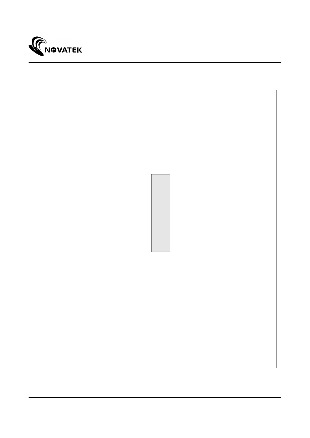
NT3980 TCP ( Top view )
DIO2
D57
D56
D55
D54
D53
D52
D51
D50
D47
D46
D45
D44
D43
D42
D41
D40
D37
D36
D35
D34
D33
D32
D31
D30
Vcc
SHL
V10
V9
V8
V7
V6
AVDD
AVSS
V5
V4
V3
V2
V1
GND
NC
CLK
LD
POL
REV1
REV2
D27
D26
D25
D24
D23
D22
D21
D20
D17
D16
D15
D14
D13
D12
D11
D10
D07
D06
D05
D04
D03
D02
D01
D00
DIO1
NT3980
OUT384
OUT383
OUT382
OUT381
OUT380
OUT5
OUT4
OUT3
OUT2
OUT1
Version 1.0 2 October 16, 2001

NT3980
nce voltage. The voltage of these pins must be AVSS< V10< V9<
pulse on DIO1 is latched at the rising edge of the
CLK. Then the data are latched serially onto internal latches at the rising edge of the CLK. After all
sing
edge of the CLK. This function can cascade two or more devices for dot expansion. In normal
applications, the DIO2 signal of the first device is connected to the DIO1 of the second stage, the
In contrast, when SHL is applied low, a start pulse inputs on DIO2, and a pulse outputs through
LD may switch the new data to outputs at anytime even if the line data are not
the polarity of the even or odd outputs.
“POL=1” indicates that even outputs are of positive polarity with a voltage range from V1~V5, and
odd outputs are of negative polarity with a voltage range from V6 to V10. On the other hand, if LD
l “POL”, even outputs are of negative polarity and odd outputs are of positive
TFT LCD Source Driver
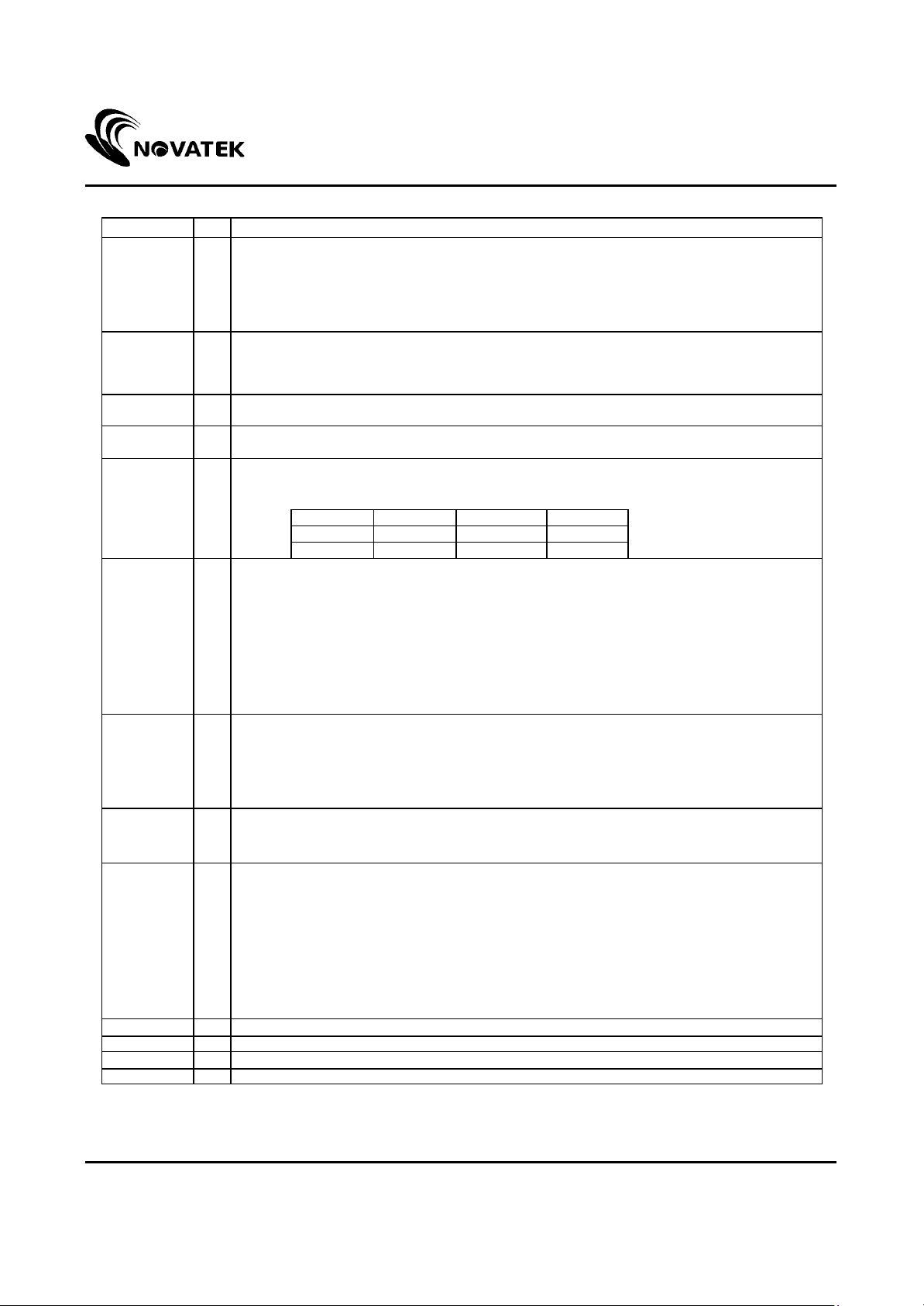
Pin Description
Designation I/O
D07 ~ D00
D17 ~ D10
D27 ~ D20
D37 ~ D30
D47 ~ D40
D57 ~ D50
REV1
REV2
V1 ~ V10 I Gamma correction refere
OUT1 ~
OUT384
SHL I
DIO1
DIO2
I Data input. For six 8-bit data,2 pixels, of color data (R, G, B)
DX7 : MSB; DX0 : LSB
I Controls whether data are inverted or not.
When “REVx”=1 the data will be inverted. EX. “00” à “ FF”, “07”à “ F8”, “15”à “EA”, and so on.
REV1: control D0x to D2x ,REV2: control D3x to D5x .
(These two pins can be connected together on TCP.)
V8<V7<V6; V5<V4<V3<V2<V1< AVDD
O Output drive signals;
Selects left or right shift;
SHL=“1” : DIO1→OUT1,2,3,4,5,6→OUT7,8,9,10,11,12--→OUT379,380,381,382,383,384= DIO2
SHL=“0” : DIO1=OUT1,2,3,4,5,6←OUT7,8,9,10,11,12←-- OUT379,380,381,382,383,384←DIO2
I/O Start pulse signal input/output
When SHL is applied high (SHL=”1”), a start high-
SHL DIO1 DIO2 SHIFT
1 Input Output Right
0 Output Input Left
Description
line latches are filled with data, 64 clocks, a pulse is shifted out through the DIO2 pin at the ri
LD I Latches the polarity of outputs and switches the new data to outputs.
CLK I Clock input; latching data onto the line latches at the rising edge .
POL I Polarity selector for the dot -inversion control. Available at the rising edge of LD.
AVDD I Power supply for analog circuit;
AVSS I Ground pin for analog circuit
Vcc I Power supply for digital circuit
GND I Ground pin for digital circuit
DIO2 of the second one is connected to the DIO1 of the third, and so on, like a daisy chain.
DIO1.
*Remark : The input pulse -width of DIO1/2 may exceed 1 clock-cycle.
1.At the rising edge, the pin latches the “POL” signal to control the polarity of the outputs.
2.This pin also controls the switch of the line registers that switches the new incoming data
to outputs.
*Remark: The
completely full.
After a start pulse input, display data latching is halted automatically after 64 clock cycles.
*Remark: At least one CLK cycle is necessary during the high-level period of LD.
“POL” value is latched at the rising edge of “LD” to control
receives low leve
polarity.
POL=1: Even outputs range from V1 ~ V5
Odd outputs range from V6 ~ V10
POL=0: Even outputs range from V6 ~ V10
Odd outputs range from V1 ~ V5
Version 1.0 3 October 16, 2001

NT3980
TFT LCD Source Driver
Power on/off sequence:
This IC is a high-voltage LCD driver, so it may be damaged by a la rge current flow when an incorrect power sequence is used.
The recommended connection sequence is to first connect the logical power, Vcc & GND and then connect the drive power,
AVDD&AVSS with V1~V10. When shutting off the power, first shut off the drive power and then the logic system, or turn off all
power simultaneously.
Relationship between the order of input data and output channels
(1) SHL=”1”, shift right, a start pulse from DIO1
Output OUT1 OUT2 OUT3 OUT4 OUT5 OUT6 - - -
Order First data --à Last data
Data D07~D00 D17~D10 D27~D20 D37~D30 D47~D40 D57~D50 - - - D57~D50
(2) SHL=”0” , shift left, a start pulse from DIO2
Output OUT379 OUT380 OUT381 OUT382 OUT383 OUT384 - - - OUT6
Order First data --à Last data
Data D07~D00 D17~D10 D27~D20 D37~D30 D47~D40 D57~D50 - - - D57~D50
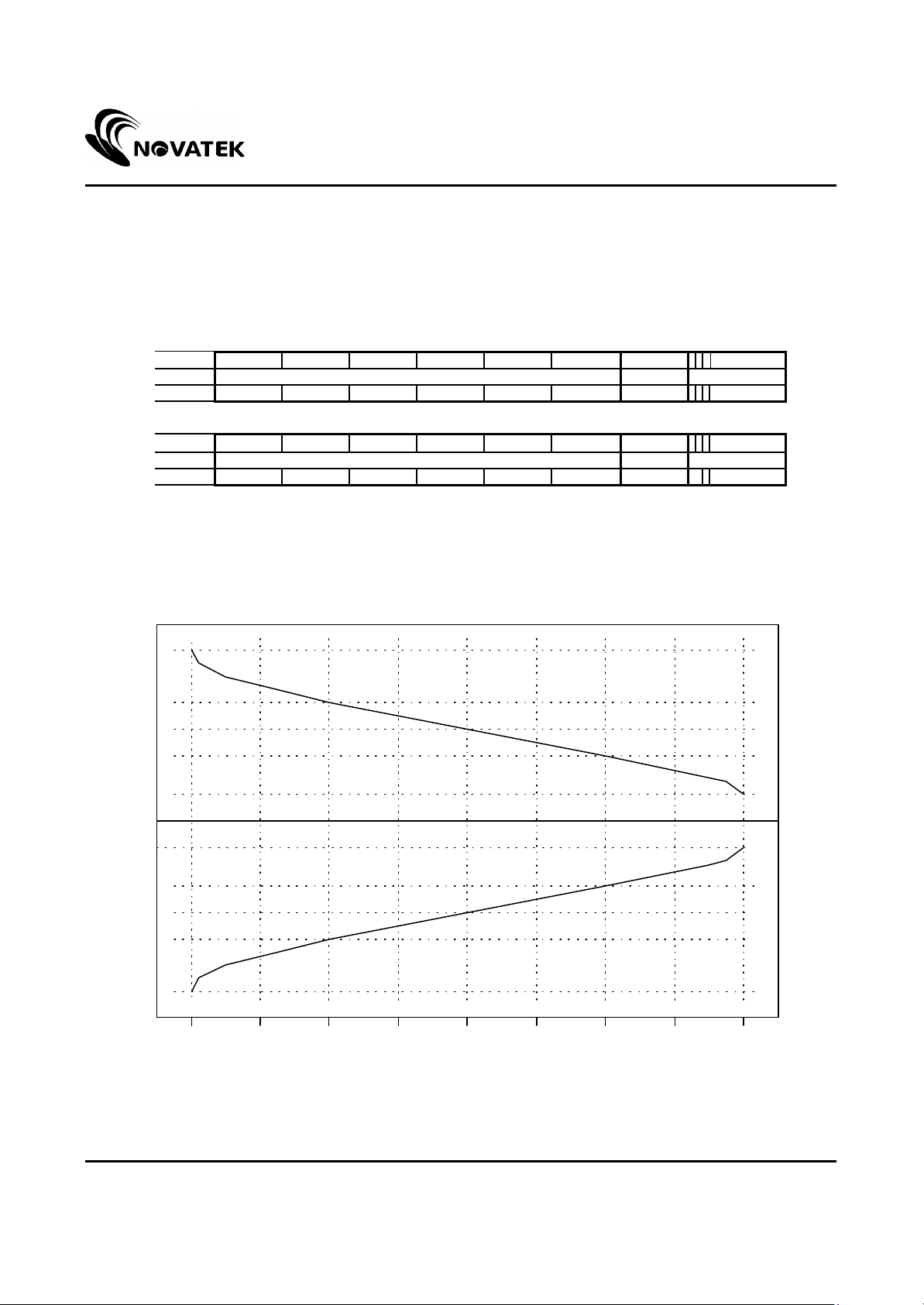
Relationship between input data and output voltage
The figure below shows the relationship among the input data and the output voltage and the polarity. The range of V1~V5 is
for positive polarity, and V6 ~ V10 for negative polarity. Please refer to the following page to get the relative resistors value and
voltage calculation method.
OUT384
Gamma correction diagram
Vout
AVDD
V1
V2
V3
V4
V5
Vcom
V6
V7
V8
V9
V10
AVSS
Remark : AVDD -0.1>V1>V2>V3>V4>V5>AVDD/2; AVDD/2>V6>V7>V8>V9>V10>0.1
Positive polarity
Negative polarity
31
6300 95 127 159 191 223 255
Input Data
Version 1.0 4 October 16, 2001
 Loading...