NOVATEK NT3966 Datasheet

NT3966
TFT LCD Source Driver
Features
n Output : 420 output channels
n 6-bit resolution /64 gray scale
n Dot inversion with polarity control
n V1 ~ V10 for adjusting Gamma correction
n Power for analog circuit : 6.5 ~ 10 V
n Output dynamic range : 0.1 ~ AVDD-0.1V
n Power consumption of analog circuit : 3mA
General Description
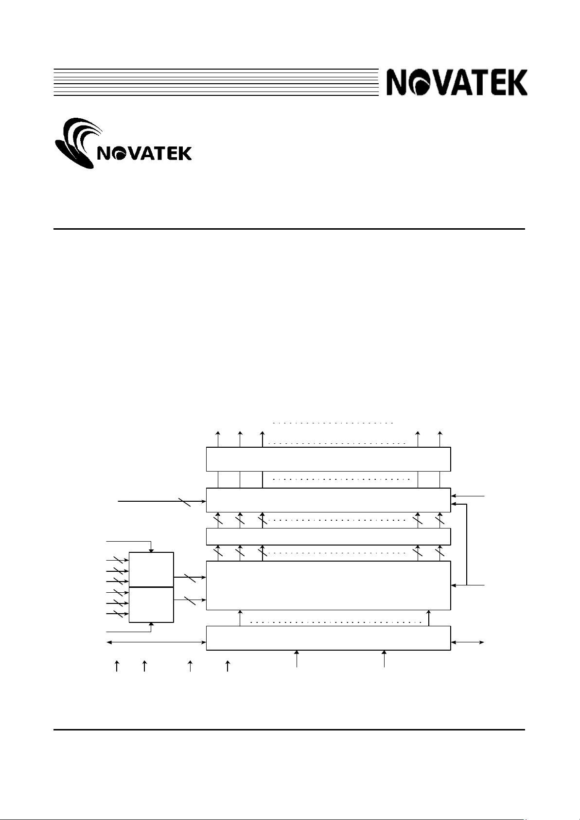
The NT3966 is a data driver IC for a color TFT LCD panel, SXGA+(1400*1050) applications. For better performance, dot
inversion and a wide range voltage output have been designed into this chip, and for reducing EMI, data inversion control has
been incorporated. This chip supplies 10 sections of voltage-reference for Gamma correction.
Block diagram
OUT1
OUT2
OUT3
n Power for interface circuit : 2.5~3.6V
n Operating frequency : 65MHz
n Output deviation : 10 ~ 20mV
n Data inversion for reducing EMI
n Cascade function with bi-direction shift control
n CMOS silicon gate ( p-type substrate )
n TCP package
OUT420
OUT419
Out Driver Buffer ( 420 channels )
V1 ~ V10
REV1
D00 ~ D05
D10 ~ D15
D20 ~ D25
D30 ~ D35
D40 ~ D45
D50 ~ D55
REV2
DIO1 DIO2
6
6
Decoder
6
6
6
Decoder
6
Vcc GND AVDD AVSS
10
6
6
18
18
Digit to Analog Converter
6
6
6
Level Shift
6666
Line Latch ( 420 X 6 bits X 2 )
1 64
70-bit Shift Register
CLK
SHL
6
POL
LD
Version 1.0 1 DEC 7 ,2001

NT3966
TFT LCD Source Driver
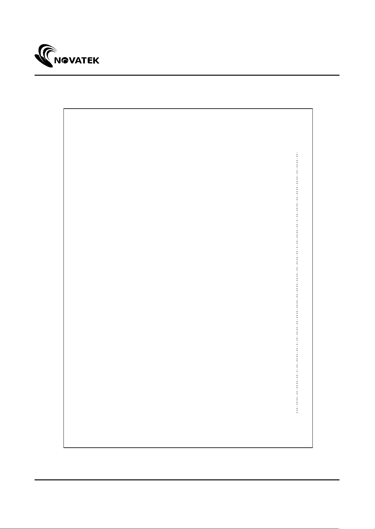
NT3966 Pads configuration (Face up): This figure does not specify the TCP package.
DIO2
D55
D54
D53
D52
D51
D50
D45
D44
D43
D42
D41
D40
D35
D34
D33
D32
D31
D30
Vcc
SHL
V10
V9
V8
V7
V6
AVDD
AVSS
V5
V4
V3
V2
V1
GND
CLK
LD
POL
REV1
REV2
D25
D24
D23
D22
D21
D20
D15
D14
D13
D12
D11
D10
D05
D04
D03
D02
D01
D00
DIO1
OUT420
OUT419
OUT418
OUT417
OUT416
NT3966
OUT5
OUT4
OUT3
OUT2
OUT1
Version 1.0 2 DEC 7 ,2001

NT3966
“2A”, and so on.
age of these pins must be AVSS< V10< V9<
ched at the rising edge of the
CLK. Then the data are latched serially onto internal latches at the rising edge of the CLK. After all
line latches are filled with data, 70 clocks, a pulse is shifted out through the DIO2 pin at the rising
size expansion. In normal
applications, the DIO2 signal of the first device is connected to the DIO1 of the second stage, the
In contrast, when SHL is applied low, a start pulse inputs on DIO2, and a pulse outputs through
o outputs at anytime even if the line data are not
tputs.
“POL=1” indicates that even outputs are of positive polarity with a voltage range from V1~V5, and
odd outputs are of negative polarity with a voltage range from V6 to V10. On the other hand, if LD
ive polarity and odd outputs are of positive
TFT LCD Source Driver
Pin Description
Designation I/O
D05 ~ D00
D15 ~ D10
D25 ~ D20
D35 ~ D30
D45 ~ D40
D55 ~ D50
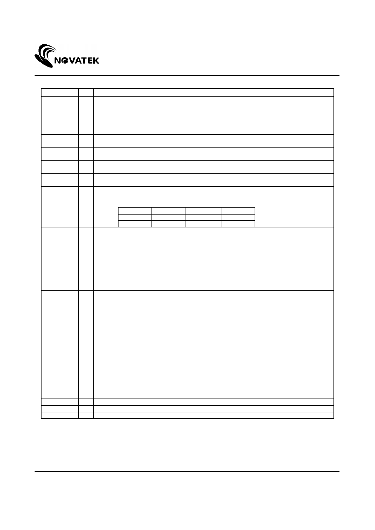
REV1 I Controls whether the data of D00~D25 are inverted or not.
REV2 I Controls whether the data of D30~D55 are inverted or not, same as REV1.
CLK I Clock input; latching data onto the line latches at the rising edge.
V1 ~ V10 I Gamma correction reference voltage. The volt
OUT1 ~
OUT420
SHL I
DIO1
DIO2
I Data input. For six 6-bit data,2 pixels, of color data (R, G, B)
DX5 : MSB; DX0 : LSB
When “REV1”=1 these data will be inverted. EX. “00” à “ 3F”, “07” à “ 38”, “15”à
V8<V7<V6; V5<V4<V3<V2<V1< AVDD
O Output drive signals;
Selects left or right shift;
SHL=“1” : DIO1→OUT1,2,3,4,5,6→OUT7,8,9,10,11,12--→OUT415,416,417,418,419,420= DIO2
SHL=“0” : DIO1=OUT1,2,3,4,5,6←OUT7,8,9,10,11,12←-- OUT415,416,417,418,419,420←DIO2
I/O Start pulse signal input/output
When SHL is applied high (SHL="1"), a start high-pulse on DIO1 is lat
SHL DIO1 DIO2 SHIFT
1 Input Output Right
0 Output Input Left
Description
LD I Latches the polarity of outputs and switches the new data to outputs.
POL I Polarity selector for the dot -inversion control. Available at the rising edge of LD
AVDD I Power supply for analog circuit
AVSS I Ground pin for analog circuit
Vcc I Power supply for digital circuit
GND I Ground pin for digital circuit
edge of the CLK. This function can cascade two or more devices for dot DIO2 of the second one is connected to the DIO1 of the third, and so on, in a chain.
DIO1.
*Remark: The input pulse-width of DIO1/2 may exceed 1 clock-cycle.
1. At the rising edge, the pin latches the “POL” signal to control the polarity of the outputs.
2. The pin also controls the switch of the line registers that switches the new incoming data
to outputs.
*Remark: The LD may switch the new data t
completely full.
“POL” value is latched at the rising edge of “LD” to control the polarity of the even or odd ou
receives low level “POL”, even outputs are of negat
polarity.
POL=1: Even outputs range from V1 ~ V5
Odd outputs range from V6 ~ V10
POL=0: Even outputs range from V6 ~ V10
Odd outputs range from V1 ~ V5
Version 1.0 3 DEC 7 ,2001

NT3966
Input Data
TFT LCD Source Driver
Power on/off sequence:
This IC is a high-voltage LCD driver, so it may be damaged by a large current flow when an incorrect power sequence is used.
The recommended sequence should be: digital power (Vcc&GND)è logic signalsèanalog power (AVDD&AVSS) èGamma
correction reference voltage(V1~V10). Reverse this sequence to shut down, or turn off all signals and power simultaneously.
Relationship between the order of input data and output channels
(1) SHL=”1”, Start pulse from DIO1, shift right
Output OUT1 OUT2 OUT3 OUT4 OUT5 OUT6 - - - OUT420
Order First data --à Last data
Data D05~D00 D15~D10 D25~D20 D35~D30 D45~D40 D55~D50 - - - D55~D50
(2) SHL=”0”, Start pulse from DIO2, shift left
Output OUT415 OUT416 OUT417 OUT418 OUT419 OUT420 - - - OUT6
Order First data --à Last data
Data D05~D00 D15~D10 D25~D20 D35~D30 D45~D40 D55~D50 - - - D55~D50
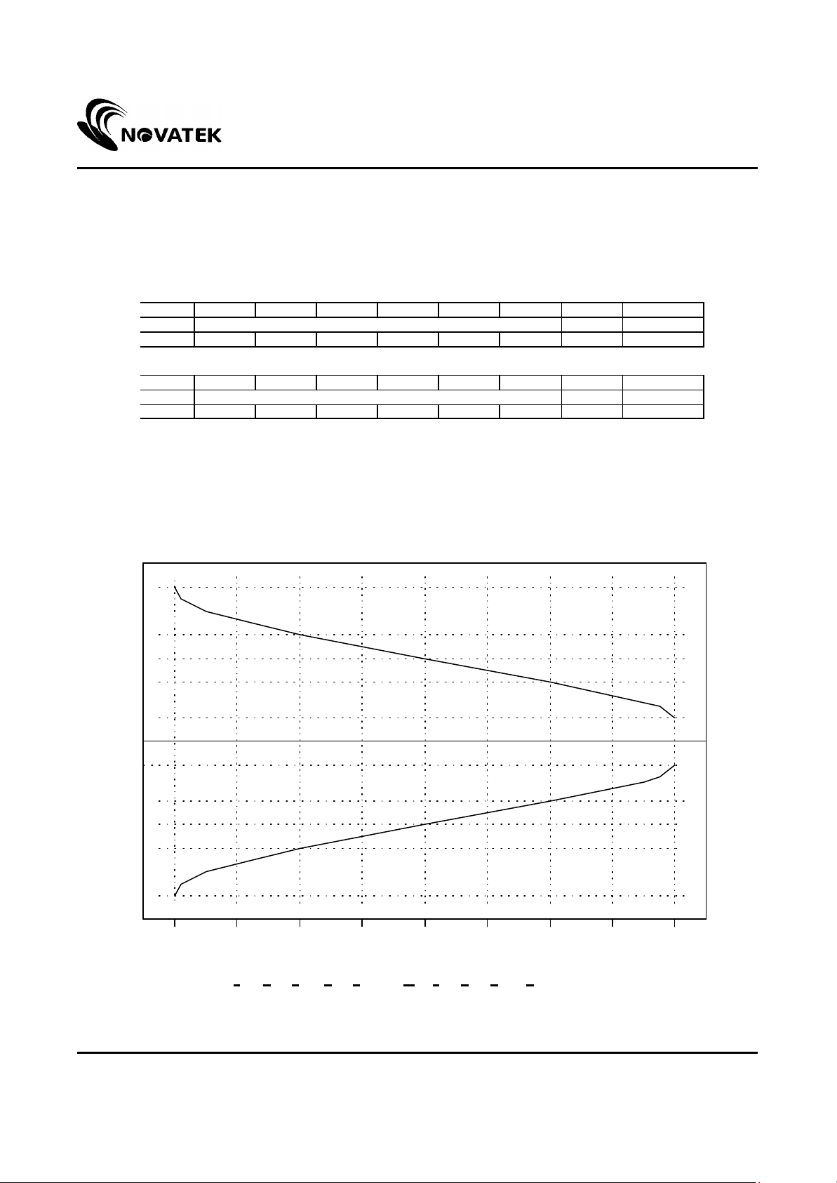
Relationship between input data and output voltage
The figure below shows the relationship among the input data and the output voltage and the polarity. The range of V1~V5 is
for positive polarity, and V6 ~ V10 for negative polarity. Please refer to the following page to get the relative resistor value and
voltage calculation method.
Gamma correction diagram
Vout
AVDD
V1
V2
V3
V4
V5
Vcom
V6
V7
V8
V9
V10
AVSS
08H
10H00H 18H 20H 28H 30H 38H 3FH
Positive polarity
Negative polarity
Remark: AV DD-0.1 > V1 > V2 > V3 > V4 > V5; V6 > V7 > V8 > V9 > V10 >AVSS+0.1V
Version 1.0 4 DEC 7 ,2001
 Loading...