NOVATEK NT3882H, NT3882F Datasheet

Dot Matrix LCD 40-Channel Driver
Features
Provides a 40 channel LCD driver
Internal serial to parallel conversion circuits:
20-bit shif t r egister X 2
40-bit lat ch X 1
40-bit 4 level driver X 1
Logic circuit supply voltage range: 4.5V - 5.5V
General Description
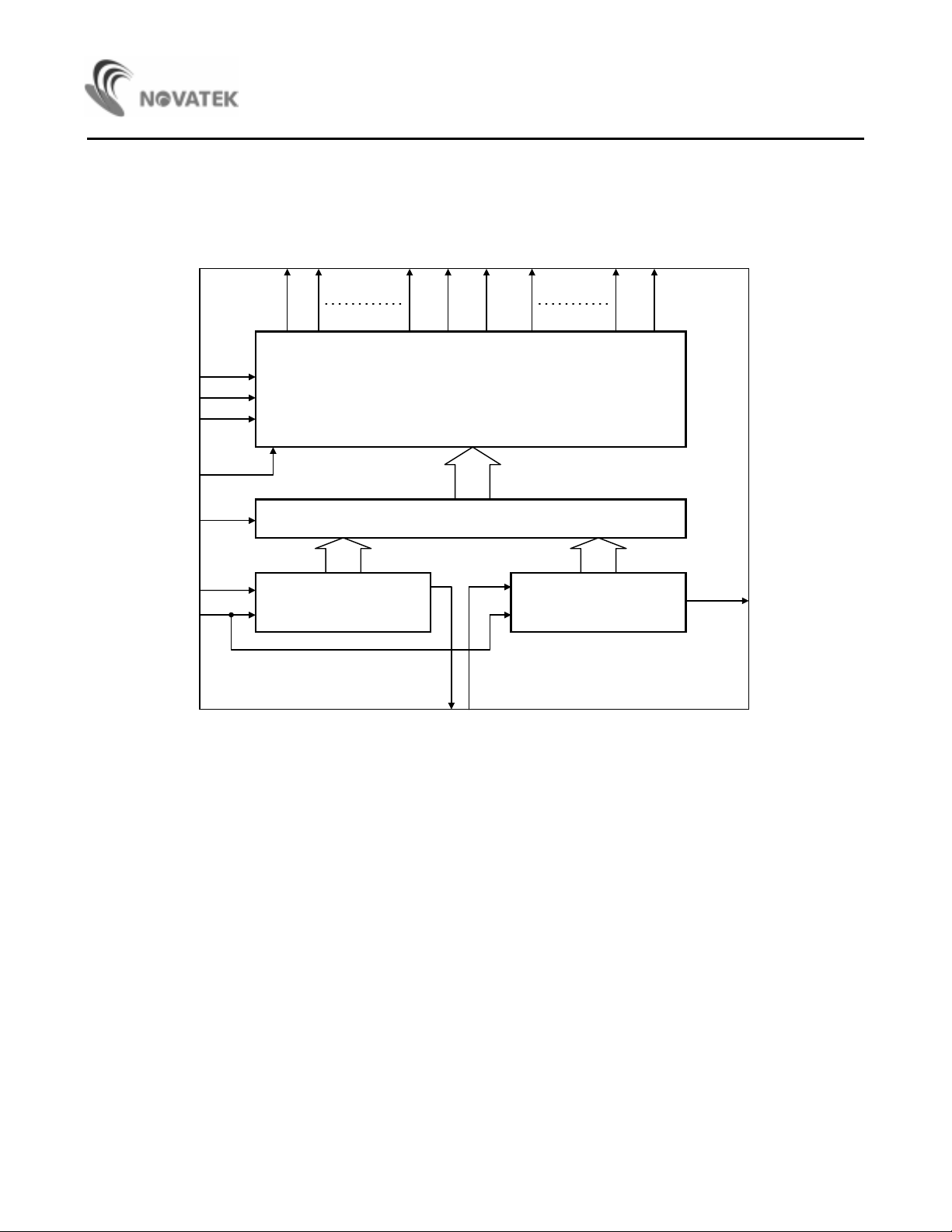
The NT3882 is a dot matrix LCD 40 channel driver
fabricated by low power CMOS technology. This IC
consists of two 20-bit shift registers, a 40-bi t l atch, and a
40-bit 4 level LCD driver. The NT3882 converts serial
data which is received from the LCD controller
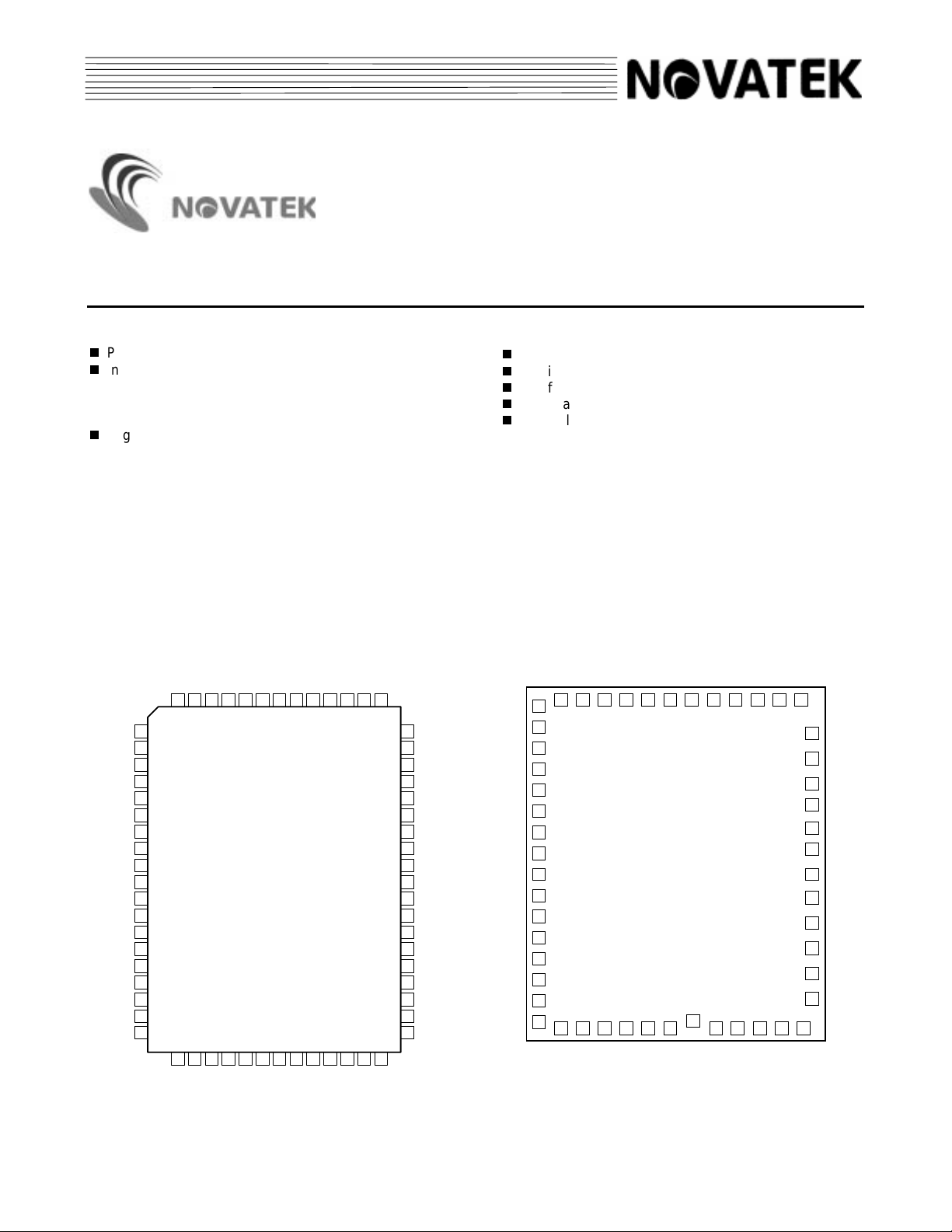
Pin Configuration Pad Configuration
LCD driving voltage range (V
Applicable LCD duty cycle: 1/2 to 1/16
Interfaces with a NT3881C/D LCD controller
LCD bias voltage can be supplied externally
Available in 64-pi n Q FP and i n CHIP FO RM
(NT3881C/D) to parallel data and then outputs LCD
driving waveforms to drive LCD. Expansion of charactertype liquid crystal display can be easily obtained
according to the number and str uct ur e of charact ers.
NT3882
DD
- VEE): 3.5V to 11V
S29
S28
S27
S26
S25
S24
S23
S22
S21
S20
S19
S18
S17
S16
S15
S14
S13
S12
S
3
N
3
3
C
4
1
2
3
4
5
6
7
8
9
10
11
12
13
14
15
16
17
18
19
20 21 22 23 24 25 26 27 28 29 30 31 32
S9S
S
1
1
0
1
3
3
3
0
1
2
NT3882F
S8S7V
D
D
C
NCS6S5S4S3S2S
3
3
35N
7
6
S
S
S
S
S
S
S
S
S
S
4
3
3
0
9
8
52535455565758596061626364
V
51NC
2
NC
50
NC
49
V
48
3
NC
47
V
46
EE
NC
45
NC
44
NC
43
M
42
NC
41
DR2
40
DL2
39
DR1
38
DL1
37
GND
36
CL2
35
CL1
34
NC
33
1
S28
S27
S26
S25
S24
S23
S22
S21
S20
S19
S18
S17
S16
S15
S14
S13
S
2
9
2 6362616059575655545352
3
4
5
6
7
8
9
10
11
12
13
14
15
16
17
18
19 20 21 22 23 24 27 28 29 30 31
S
1
2
3
4
S9S
3
3
2
3
S
1
1
0
1
NT3882H
3
3
0
1
S8S7V
3
5
25
D
D
3
3
3
8
7
6
S6S5S4S3S
4
3
0
9
V
51
2
V
48
3
V
46
EE
M
42
DR2
40
DL2
39
DR1
38
DL1
37
GND
36
CL2
35
CL1
34
S1
32
2
S
S
S
S
S
S
S
S
S
S
S
1 V2.0 November, 1999

Block Diagram
g
V
DD
V
2
V
3
V
EE
M
NT3882
S1 S2 S19 S20 S21 S22 S39 S40
40-Bit 4-Level LDC Drivers
CL1
DL2
CL2
20-Bit Shift
Re
ister
40-Bit Latch
20-Bit Shift
Register
DR2
GNDDL2DR1
2

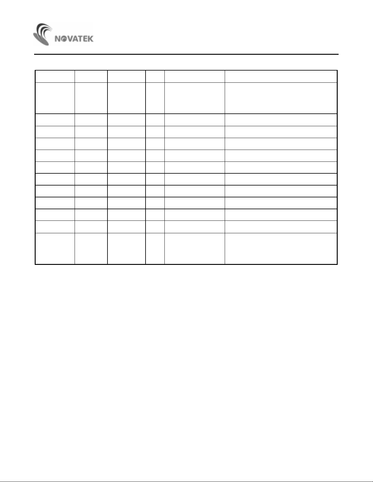
Pin and P ad Descriptio ns
Pin No. Pad No. Designation I/O External Connection Description
NT3882
2- 24,
27 - 32,
52 - 57,
59 - 63
25 25
27 - 32,
2 - 24,
52 - 57,
59 - 63
S29 - S7,
S6 - S1,
S40 - S35,
S30 - S34
DD
V
O LCD panel Segment signal output pi ns
P Power supply Power for logic circui t s
34 34 CL1 I Controller Clock to latch serial data
35 35 CL2 I Controller Clock to shift serial dat a
36 36 GND P Power Supply 0V
37 37 DL1 I Controlleror NT3882 Data input of 1 - 20 bits from controller
38 38 DR1 O NT3882 Data output of 20 bit shift register
39 39 DL2 I Controlleror NT3882 Data input of 21 - 40 bits from controller
40 40 DR2 O NT3882 Data output of 40 bit shift register
42 42 M I Controller Alternate signal for LCD dri vers
46, 48, 51 46, 48, 51
V
EE
, V3, V
P Power Supply Power for LCD drivers
2
1, 26, 33, 41,
43 - 45, 47,
- NC - - No connection
49, 50, 58,
64
Functional Description
NT3882 is a dot matrix LCD segment driver LSI. It
operates with the controller, such as NT3881C/D, and/ or
another segment driver LSI NT3882. NT3882 receives
serial data from the controller or another NT3882,
converts it to parallel data and then supplies the LCD
driving waveform s t o t he LCD panel.
1. CL1
This signal is used for latchi ng t he shi f t register contents.
When CL1 is set at high, the shift register contents are
transferred to the 40-bit 4level LCD driver. W hen CL1 is
set at low, the last display output data (S1 to S40) is
held.
2. CL2
Clock pulse inputs for the two 20-bit shif t registers. The
data is shi f ted to a 40-bit latch at the falli ng edge of CL2.
The clock singal CL2 must be active when operating to
refresh shift registers' contents.
3. DL1
The 1 - 20 bit data from LCD controller is fed into the
first 20-bit shift r egister thr ough DL1.
4. DR1
The 20th bit data of first 20-bit shift register output from
DR1. The data shifted out from DR1 after 20 bit delay
are synchronized with the clock pulse (CL2). By
connecting DR1 to DL2, two 20-bit shif t registers can be
cascaded to one 40-bit shift register.
5. DL2
The 21 - 40 bit data from the LCD control ler is fed into
the second 20-bit shift register through DL2.
6. DR2
The 40th bit data of the second 20-bit shift register
output is fr om DR2. The data shift ed out from DR2 after
a 20-bit delay i s synchronized with the clock pulse ( CL2).
By connecting DR2 to the next NT3882 DL1, the cascade
construction i s obt ained to drive a wider LCD panel.
7. S1 to S40
These 40 bits represent the 40 data bits in the 40-bit
DD
latch. One of V
, V2, V3 and VEE is selected as a LCD
driving voltage source according to the combination of
latched data level and the alternate signal (M).
3
 Loading...