

INSTRUMENTS
INSTRUCTION MANUAL
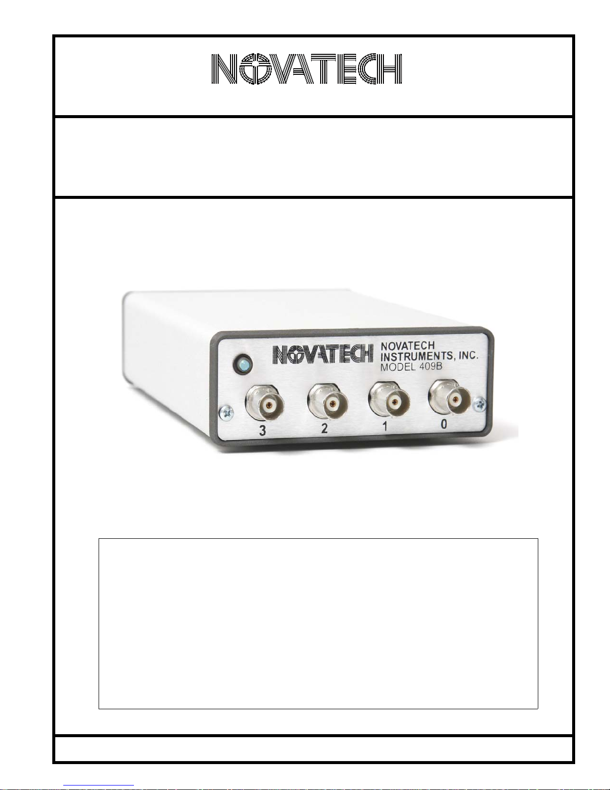
Model 409B 171 MHz 4-Channel Signal Generator
Section Page Contents
1.0 . . . . . . . . . . . . . . . . . . . . . . . . . . . . . 2 . . . . . . . . . . . . . . . . . . . . . . . . . Description
2.0 . . . . . . . . . . . . . . . . . . . . . . . . . . . . . 2 . . . . . . . . . . . . . . . . . . . . . . . Specifications
3.0 . . . . . . . . . . . . . . . . . . . . . . . . . . . . . 2 . . . . . . . . . . . . . . . . . Hardware Installation
4.0 . . . . . . . . . . . . . . . . . . . . . . . . . . . . . 5 . . . . . . . . . . . . . . . . . . . . . . . . . . .Operation
5.0 . . . . . . . . . . . . . . . . . . . . . . . . . . . . . 6 . . . . . . . . . . . . . . . . . . Theory of Operation
6.0 . . . . . . . . . . . . . . . . . . . . . . . . . . . . . 8 . . . . . . . . . . . . . . . . . . . . .Performance Test
7.0 . . . . . . . . . . . . . . . . . . . . . . . . . . . . . 9 . . . . . . . . . . . . . . . . . . . . . . . . . .Calibration
8.0 . . . . . . . . . . . . . . . . . . . . . . . . . . . . .10 . . . . . . . . Appendix A: Table Mode Details
9.0 . . . . . . . . . . . . . . . . . . . . . . . . . . . . .12 . . . . . . . . Appendix B: External Reference
--. . . . . . . . . . . . . . . . . . . . . . . . . . . . . . .13 . . . . . . . . . . . . . . . . . . . . . . . . . . . Warranty
NOVATECH INSTRUMENTS 1 409B Manual, 17-Apr-2015
Model 409B
Table of Contents

1.0 DESCRIPTION
1.1 The Model 409B is a four-channel Direct Digi-
tal Synthesizer (DDS) in a small table top case with
RS232 serial control. The 409B provides four independent, phase-synchronous sine wave (consult factory for LVCMOS) output signals, which can be set
from 0.0 Hz (DC) to 171 MHz in 0.1 Hz steps when
using the internal VCTCXO clock.
1.2 The 409B can also be used with an External
Clock input. An on-board programmable frequency
multiplier generates the master clock allowing user
configured frequency ranges. The multiplier can be
disabled for direct inputs up to 500 MHz for optimum phase noise performance. When used with the
same external clock source, multiple 409B are phase
synchronous.
1.3 The /R option converts the External Clock input
to a 10.00 MHz reference input. Using the same
topology as our locking programmable oscillator
modules, this options allows locking to and tracking
of an external 10.00 MHz, with no binary round-off
errors. When this option is installed the accuracy
and stability of the output are equal to those of the
reference.
2.0 SPECIFICATIONS
2.1 OUTPUTS
TYPES: Four Sine simultaneously (four independent,
phase-synchronous outputs.)
IMPEDANCE: Sine: 50 Ω; LVCMOS : 50 Ω.
RANGE: 0.0 Hz to 171 MHz in 0.1 Hz steps (Sine out, int.
clock).
SINE AMPLITUDE: approximately 1 V
50Ω. Programmable from 0/1024 to 1023/1024 of Full
Scale (10-bits), or by scale factors of 1/2, 1/4, or 1/8.
PHASE: Each channel 14-bits programmable (0.022
FLATNESS: ±3dB from 1 kHz to 150 MHz referenced to
amplitude at 35 MHz, full scale.
2.2 LVCMOS AMPLITUDE
Voh >=2.4V and Vol <=0.4V when series terminated. Rise
and fall times <1.5ns. (>1 MHz, <125 MHz) (consult fac-
tory for LVCMOS)
(+4dBm) into
pp
o
).
or direct connection to the DDS generator. All settings
(except table mode data) can be saved in non-volatile
(EEPROM) memory via the RS232 port.
2.4 ACCURACY AND STABILITY
Accuracy: <±1.5ppm at 10 to 40oC. Stable to an addi-
o
tional ±1ppm per year, 18 to 28
C. (Internal Clock)
2.5 EXTERNAL CLOCK IN
LEVEL: 0.2 to 0.5 Vrms Sine or Square Wave. 50 Ω.
FREQUENCY: 10 MHz to 125 MHz with multiplier of 4 to
20 enabled. Direct input of 1 MHz to 500 MHz.
/R Option: 10.00 MHz, ±5ppm. Automatically detected.
Internal clock is locked to and tracks this value.
2.6 SPECTRAL PURITY (Typ. 50Ω load, internal
clock, full-scale output)
Phase Noise: <-120dBc, 10kHz offset, 10 MHz out.
Spurious: <-60dBc below 10 MHz (typ. 300MHz span)
<-60dBc below 40 MHz
<-55dBc below 80 MHz
<-50dBc below 160 MHz
Harmonic: <-65dBc below 1 MHz
<-55dBc below 20 MHz
<-45dBc below 80 MHz
<-35dBc below 160 MHz
(channel-channel isolation: <-60dBc)
2.7 TABLE MODE
On-board 4Mb static ram holds up to 32,768 profile
points in table mode allowing a different output in 100 µS
increments.
2.8 POWER REQUIREMENTS
+4.5 to +5.5 VDC <1Amp. AC adapter provided.
2.9 SIZE
39mm H, 107mm W, 172mm L, not including connectors.
2.10 CONNECTORS
BNC for Sine Outputs and EXT CLK IN. DE9 for Serial
Control. 2.5mm center positive power receptacle for +5
volts input. AC-adapter provided.
2.11 OPTIONS
Model 409B-AC adds two rear-panel SMA connectors for
external control of output update and table timing (see
AN002). /R Option converts the External Clock In to a
10.00 MHz external reference input (see Appendix B).
2.3 CONTROL
Output frequencies, amplitudes (10-bits) and phases (14bits) are controlled by an RS232 serial port at 19.2kbaud,
NOVATECH INSTRUMENTS 2 409B Manual, 17-Apr-2015

3.0 HARDWARE INSTALLATION
3.1 Power Connection. The required power of
+5Volts DC is applied through a 2.5mm center-positive power connector (Switchcraft 712A or equivalent). The Novatech Instruments, Inc. supplied ACadapter comes complete with the correct mating
connector.
WARN I NG:
Use of an unregulated source may damage the 409B.
Use only the provided AC-adapter or consult
Novatech Instruments, Inc. for application
assistance if you wish to use another power source.
3.2 The quality of your power supply affects the
performance of the 409B. The supply should be free
of ripple and noise (<50mV). Even though extensive
filtering is used internal to the 409B, a quiet and
well regulated power supply will ensure optimum
performance. The supplied AC-adapter has been
tested for proper operation.
3.3 Installation. To use the 409B, connect your
host computer to the 9-pin female RS232 connector
on the rear panel of the 409B. If you are using a PC,
a 9-pin monitor extension cable used as an RS232
cable will allow direct connection to the 409B without the use of a null modem cable or gender changer.
If you are using a different computer, terminal or
other control source, please note that the data TO
the 409B is on pin 3; the data FROM the 409B is on
pin 2 and the COMMON return is on pin 5. Set your
host to 19.2 kBaud, 8 bits, 1 stop bit, no parity and
no hardware flow control. See Table 2 for Serial
Commands.
3.4 A USB to RS232 adapter cable is available for
use with computers that do not provide a serial port.
Follow the manufacturer’s installation instructions
when using a USB adapter.
3.5 Commands are not case sensitive. There must
be a space after each command except R, CLR, S
and QUE. End with any combination of CR, LF or
CRLF. Illegal commands will result in an error
code being returned per Table 1.
Table 1: RS232 Error Codes
Error Code Meaning
OK Good command received
?0 Unrecognized Command
?1 Bad Frequency
?2 Bad AM Command
?3 Input line too long
?4 Bad Phase
?5 Bad Time
?6 Bad Mode
?7 Bad Amp
?8 Bad Constant
?f Bad Byte
3.6 The “QUE” command returns five hexadecimal
strings reflecting the present state of the 409B. See
page 7 for an explanation of the values that make up
these strings. Note that the frequency settings will be
scaled as discussed below if an external clock is
used.
3.7 The “B” command can cause erroneous operation and must be used with care. Contact Novatech
Instruments, Inc. for application assistance if you
wish to use this command. Detailed knowledge of
the operation of the Analog Devices AD9959 DDS
generator is required.
NOTE:
The program SOF8 is supplied with the 409B. This
program provides a graphical interface for all the
serial commands, allowing simple control of the
409B.
3.8 Internal Clock. If you plan to use the 409B
internal clock, which is the default setup mode, no
action is required. If the 409B was previously set to
use the external clock, send the serial command “C
i” to reselect the internal clock. If you wish to
maintain this setting, use the save command “S”.
3.9 External Clock. If you are providing your own
clock source, send the serial command “C e”.
Apply your clock to the External Clock Input BNC
on the rear panel. Note that phase noise and stability
NOVATECH INSTRUMENTS 3 409B Manual, 17-Apr-2015
RS232 Command Function
Fn xxx.xxxxxxx Set Frequency of output “n” in MHz to nearest 0.1 Hz. Decimal point required. Set
Pn N
Vn N Set voltage level of output “n”. In default, the amplitude is set to the maximum:
E x Serial echo control. x=D for Echo Disable, x=E for Echo Enable
C x Select clock source. x=E for External clock, x=I for Internal Clock. May require
R Reset. This command resets the 409B. EEPROM data is preserved and, if valid, is
CLR Clear. This command clears the EEPROM valid flag and restores all factory
A x x=E for LVCMOS Enable, x=D for LVCMOS Disable. (consult factory for
S Saves current state into EEPROM and sets valid flag. State used as default upon
QUE Return present frequency, phase and status. Returns a character string of all inter-
M N Mode command. Mode ‘0’ is single tone on all channels (default). If N=a, then the
Vs N Set the output Voltage scaling factor. N=1 for full scale, N=2 for one-half scale,
Kp aa Set PLL reference multiplier constant. Must be one Hexadecimal byte as two
I x Set the I/O update pulse method. If x=a, then an I/O update is issued at the end of
B aa[bb[cc[dd[ee[ff[gg]]]]]]
Table 2 : Serial Commands
to 0.00 to turn off a channel. n=0, 1, 2, 3. Maximum setting: 171.1276031 MHz.
Single tone mode.
Set Phase of output “n”. N is an integer from 0 to 16383. Phase is set to N*360
16384 or N*π/8192 radians. Sets the relative phase of the frequency output
depending upon the value of n=0, 1, 2, 3. Single tone mode.
approximately 1V
decimal point allowed). Voltage level is scaled by N/1023. n=0, 1, 2, 3 to set the
amplitude on frequency 0, 1, 2 or 3. If N >=1024, the scaling is turned off and the
selected output is set to full scale.
adjustment of Kp and the addition of external filtering of output. (Do not use this
command if the /R option is installed)
used upon restart. This is the same as cycling power.
default values.
LV CM OS)
next power up or reset. Use the “CLR” command to return to default values.
nal settings.
phase is automatically cleared during each command; if N=n, then the phase is not
cleared (default). See Section 4.0 for details. See appendix for table mode.
N=4 for one-quarter scale and N=8 for one-eighth scale. All channels are scaled
equally.
characters. Legal values are 1 (bypass PLL) and 4 to 20 (01
Kp times clock frequency must not be between 160MHz and 255MHz (for internal
clock, this disallows 5<=Kp<= 9). (see paragraph 4.12) Not used with /R option.
each serial command (default). If x=m, then a manual I/O update pulse is sent by a
subsequent ‘I p’ command. (see section 4.0 for details)
This Byte command allows each register in the DDS chip to be set. Different
registers require a various number of bytes to be written depending upon the
function. Please consult the manual for details. Note that it is possible to set the
DDS chip into a non-functional mode, requiring a power cycle to recover. All
values are in hexadecimal and no error checking, other than correct format, is
performed.
(+4dBm) into 50Ω. N can range from 0 (off) to 1023 (no
pp
, 04h to 14h). Values of
h
o
/
NOVATECH INSTRUMENTS 4 409B Manual, 17-Apr-2015
 Loading...