

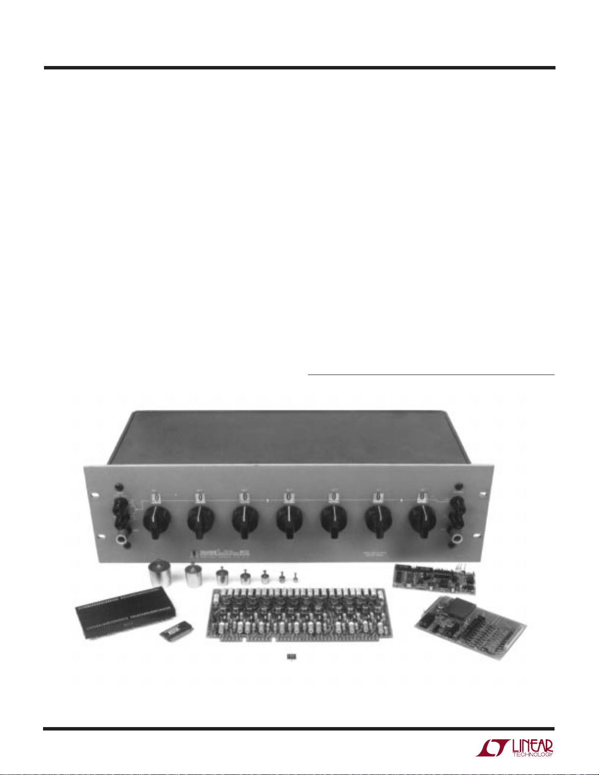
Page 1
Application Note 86
January 2001
A Standards Lab Grade 20-Bit DAC with 0.1ppm/°C Drift
The Dedicated Art of Digitizing One Part Per Million
Jim Williams
J. Brubaker
P. Copley
J. Guerrero
F. Oprescu
INTRODUCTION
Significant progress in high precision, instrumentation
grade D-to-A conversion has recently occurred. Ten years
ago 12-bit D-to-A converters (DACs) were considered
premium devices. Today, 16-bit DACs are available and
increasingly common in system design. These are true
precision devices with less than 1LSB linearity error and
1ppm/°C drift.1 Nonetheless, there are DAC applications
that require even higher performance. Automatic test
equipment, instruments, calibration apparatus, laser trimmers, medical electronics and other applications often
require DAC accuracy beyond 16 bits. 18-bit DACs have
been produced in circuit assembly form, although they are
expensive and require frequent calibration. 20 and even
23+ (0.1ppm!) bit DACs are represented by manually
switched Kelvin-Varley dividers. These devices, although
amazingly accurate, are large, slow and extremely costly.
Their use is normally restricted to standards labs.2 A
useful development would be a practical, 20-bit (1ppm)
DAC that is easily constructed and does not require
frequent calibration.
20-Bit DAC Architecture
Figure 1 diagrams the architecture of a 20-bit (1ppm) DAC.
This scheme is based on the availability of a true 1ppm
analog-to-digital converter with scale and zero drifts below 0.02ppm/°C. This device, the LTC®2400, is used as a
feedback element in a digitally corrected loop to realize a
20-bit DAC.
3
In practice, the “slave” 20-bit DAC’s output is monitored
by the “master” LTC2400 A-to-D, which feeds digital
information to a code comparator. The code comparator
differences the user input word with the LTC2400 output,
presenting a corrected code to the slave DAC. In this
fashion, the slave DAC’s drifts and nonlinearity are continuously corrected by the loop to an accuracy determined
by the A-to-D converter and V
4
. The sole DAC require-
REF
ment is that it be monotonic. No other components in the
loop need to be stable.
V
REF
20-BIT
USER
INPUT
CODE
COMPARATOR
CORRECTED
CODE
DIGITAL
CODE
Figure 1. Conceptual Loop-Based 20-Bit DAC. Digital
Comparison Allows A-to-D to Correct DAC Errors. LTC2400
A-to-D’s Low Uncertainty Characteristics Permit 1ppm
Output Accuracy
, LTC and LT are registered trademarks of Linear Technology Corporation.
Note 1: See Appendix A, “A History of High Accuracy Digital-to-Analog
Conversion,” for a review of high accuracy digital-to-analog conversion.
Note 2: Consult Appendix C, “Verifying Data Converter Linearity to
1ppm,” for discussion on Kelvin-Varley dividers. Also, see Appendix A,
“A History of High Accuracy Digital-to-Analog Conversion.”
Note 3: The LTC2400 analog-to-digital converter is profiled in
Appendix␣ B, “The LTC2400—A Monolithic 24-Bit Analog-to-Digital
Converter.”
Note 4: D-to-A converters have been placed in loops to make A-to-D
converters for a long time. Here, an A-to-D converter feeds back a loop
to form a D-to-A converter. There seems a certain justified symmetry
to this development. Turnabout is indeed fair play.
FEEDBACK
CODE
20-BIT
“SLAVE”
DAC
LTC2400
“MASTER”
A-TO-D
V
IN
20-BIT
(1PPM)
ANALOG
OUTPUT
V
OUT
AN86 F01
AN86-1
Page 2
Application Note 86
This loop has a number of desireable attributes. As mentioned, accuracy limitations are set by the A-to-D converter and its reference. No other components need be
stable. Additionally, loop behavior averages low order bit
indexing and jitter, obviating the loop’s inherent smallsignal instability. Finally, classical remote sensing may be
used or digitally based sensing is possible by placing the
A-to-D converter at the load. The A-to-D’s SO-8 package
and lack of external components makes this digitally
incarnated Kelvin sensing scheme practical.
5
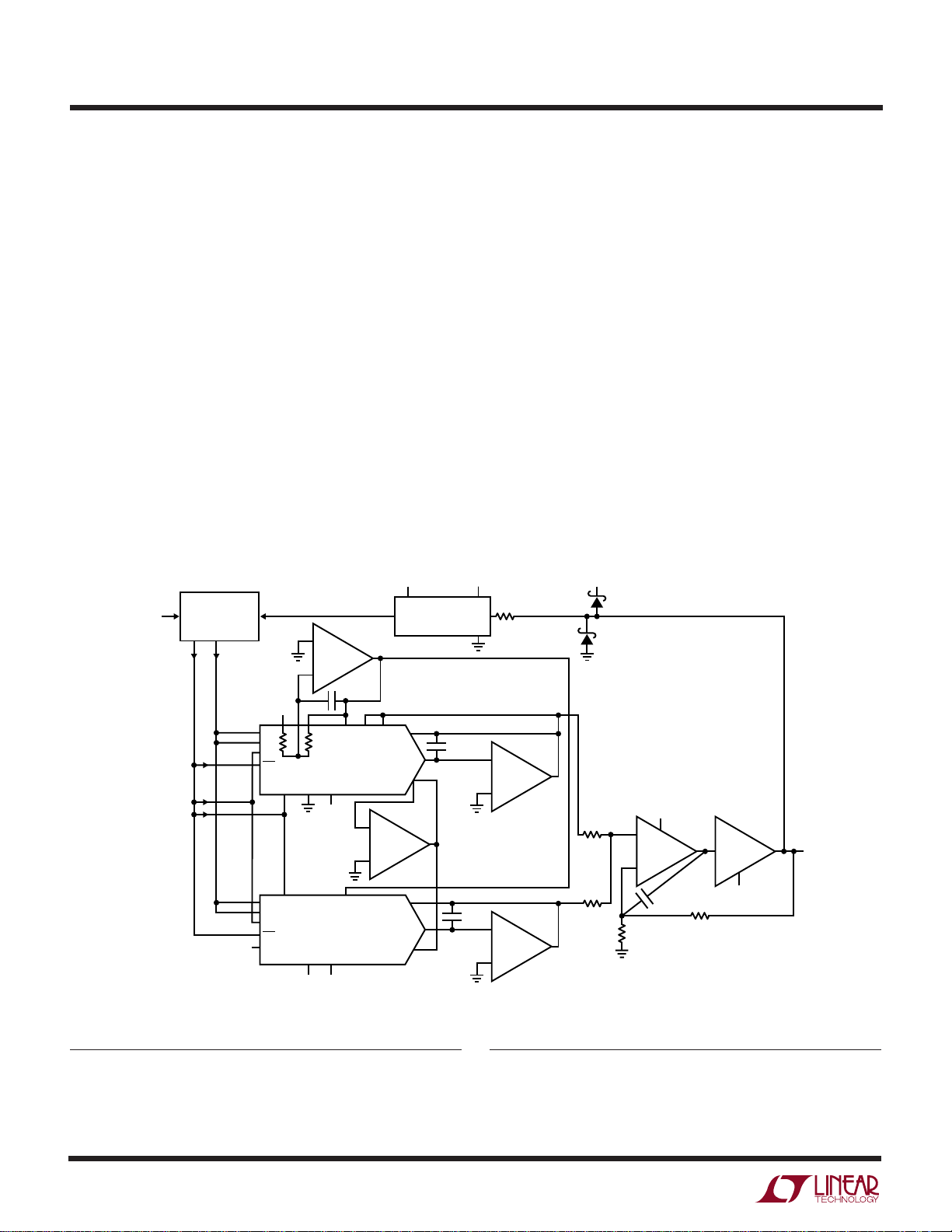
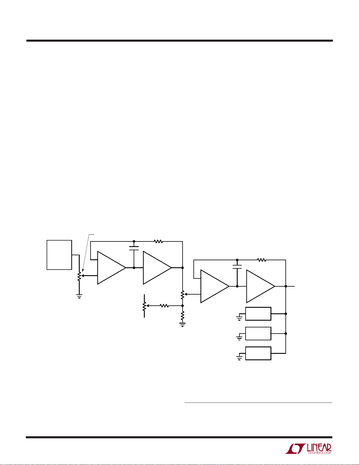
Circuitry Details
Figure 2 is a detailed schematic of the 1ppm DAC. The
slave DAC is comprised of two DACs. The upper 16 bits of
the code comparator’s output are fed to a 16-bit DAC
(“MSB DAC”), while the lower bits are converted by a
separate DAC (“LSB DAC”). Although a total of 32 bits are
presented to the two DACs, there are 8 bits of overlap,
assuring loop capture under all conditions. The composite
20-BIT
USER
INPUT
CODE
COMMAND
INPUTS FROM
CODE COMPARATOR
CODE
COMPARATOR
(SEE APPENDIX D
FOR DETAILS)
CORRECTED
CODE OUT—
24-BIT WORD
+
LT1001
–
A4
24-BIT
FEEDBACK
CODE
5V 5V
SERIAL
DIGITAL
OUT
LTC2400
A-TO-D
5V
DACs’ resultant 24-bit resolution provides 4 bits of indexing range below the 20th bit, ensuring a stable LSB of
1ppm of scale. A1 and A2 transform the DAC’s output
currents into voltages, which are summed at A3. A3’s
scaling is arranged so that the correction loop can always
capture and correct any combination of zero- and fullscale errors. A3’s output, the circuit output, feeds the
LTC2400 A-to-D. The LT®1010 provides buffering to drive
loads and cables. The A-to-D’s digital output is differenced
against the input word by the code comparator, which
produces a corrected code. This corrected code is applied
to the MSB and LSB DACs, closing a feedback loop.6 The
loop’s integrity is determined by A-to-D converter and
voltage reference errors.7 The resistor and diodes at the
5V powered A-to-D protect it from inadvertent A3 outputs
(power up, transient, lost supply, etc.). A4 is a reference
inverter and A5 provides a clean ground potential to both
DACs.
(SEE APPENDIX I
REF
FOR OPTIONS)
REF
IN
CS
1k
1N5817
1N5817
100pF
5V
LD
WR
ML
BYTE
REF
R
R
LTC1599
CLVL CLR
5V
REF R
OSRFS
–
A5
LT1001
FB
I
OUT
–
I
* = 1% METAL FILM
DATA
INPUTS
+
DATA
INPUTS
BYTE
LD
WR
5V
CLVL
LTC1599
ROSCLR
V
REF
REFML
5V
R
FB
I
OUT
–
I
Figure 2. Detail of 1ppm DAC. Composite DAC Is Comprised of Two DAC Values Summed
at Output Amplifier. LTC2400 A-to-D and Code Comparator Furnish Stabilizing Feedback
Note 5: One wonders what Lord Kelvin’s response would be to the
digizatation of his progeny. Such uncertainties are the residue of progress.
Note 6: The code comparator is detailed in Appendix D, “A Processor
Based Code Comparator.”
MSB DAC
100pF
–
A1
LT1001
+
2k*
+
LT1001
15V
A3
OUTPUT
AMPLIFIER
LT1010
–
LSB DAC
100pF
–
LT1001
4.12M*
A2
0.1µF
4.12M*
–15V
2k*
+
Note 7: Voltage reference options are discussed in Appendix I,
“Voltage References.” For tutorial on the LTC2400, refer to
Appendix␣ B.
OUTPUT
AN86 F02
AN86-2
Page 3
Application Note 86
Linearity Considerations
A-to-D linearity determines overall DAC linearity. The
A-to-D has about ±2ppm nonlinearity. In applications
where this error is permissible, it may be ignored. If 1ppm
linearity is required, it is obtainable by correcting the
residual linearity error with software techniques. Details
on LTC2400 linearity and this feature are presented in
Appendices D and E.
DC Performance Characteristics
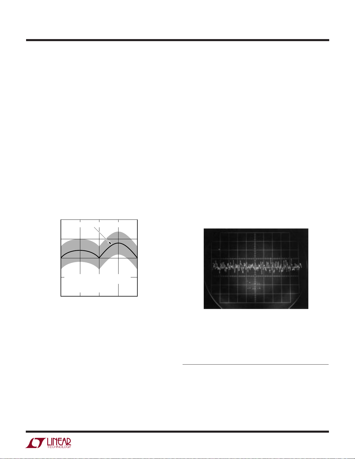
Figure 3 is a plot of linearity vs output code. The data
shows linearity is within 1ppm over all codes.8 Output
noise, measured in a 0.1Hz to 10Hz bandpass, is seen in
Figure 4 to be about 0.2LSB.9 This measurement is
somewhat corrupted by equipment limitations, which set
a noise floor of about 0.2µV.
Dynamic Performance
The A-to-D’s conversion rate combines with the loop’s
sampled data characteristic and slow amplifiers to dictate
relatively slow DAC response. Figure 5’s slew response
requires about 150 microseconds.
Figure 6 shows full-scale DAC settling time to within 1ppm
(±5µV) requires about 1400 milliseconds. A smaller step
(Figure 7) of 500µV needs only 100 milliseconds to settle
within 1ppm.
10
Conclusion
Summarized 1ppm DAC specifications appear in Figure 9.
These specifications should be considered guidelines, as
the options and variations noted will affect performance.
Consult the appropriate appendices for design specifics
and trade-offs.
1.0
INDICATED MEASUREMENT RESULTS
0.5
0
SHADED REGION DELINEATES
LINEARITY ERROR (ppm)
–0.5
MEASUREMENT UNCERTAINTY DUE TO
DAC OUPUT NOISE AND
INSTRUMENTATION LIMITATIONS
–1.0
0
262,144 524,288 786,432 1,048,576
DIGITAL INPUT CODE
Figure 3. Linearity Plot Shows No
Error Outside 1ppm for All Codes
AN86 F03
500nV/DIV
2s/DIV AN86 F04.tif
Figure 4. Output Noise Indicates Less Than 1µV,
About 0.2LSB. Measurement Noise Floor, Due
to Equipment Limitations, Is 0.2µV
Note 8: Establishing and maintaining confidence in a 1ppm linearity
measurement is uncomfortably close to the state of the art. The
technique used is shown in Appendix C, “Verifying Data Converter
Linearity to 1ppm.”
Note 9: Noise measurement considerations appear in Appendix H,
“Microvolt Level Noise Measurement.”
Note 10: Measuring DAC settling time to 1ppm is by no means
straightforward, even at the relatively slow speed involved here. See
Appendix G, “Measuring DAC Settling Time.”
AN86-3
Page 4
Application Note 86
1V/DIV
50µs/DIV AN86 F05.tif
5µV/DIV
500ms/DIV AN86 F06.tif
Figure 5. DAC Output Full-Scale Slew Characteristics Figure 6. High Resolution Settling Detail After a Full-Scale Step.
Settling Time Is 1400 Milliseconds to Within 1ppm (±5µV)
PARAMETER SPECIFICATION
Resolution 1ppm
5µV/DIV
50ms/DIV AN86 F07.tif
Figure 7. Small Step Settling Time Measures 100
Milliseconds to Within 1ppm (±5µV) for a 500µV
Transition
Full-Scale Error 4ppm of V
(Trimmable to 1ppm by V
Full-Scale Error Drift 0.04ppm/°C Exclusive of Reference
(0.1ppm/°C with LTZ1000A Reference
Offset Error 0.5ppm
Offset Error Drift 0.01ppm/°C
Nonlinearity ±2ppm, Trimmable to Less Than 1ppm
Output Noise 0.2ppm
(≈0.9µV, 0.1Hz to 10Hz BW)
Slew Rate 0.033V/µs
Settling Time—Full-Scale Step 1400 Milliseconds
Settling Time—500µV Step 100 Milliseconds
Output Voltage Range 0V to 5V. For Other Ranges See Note 3
Note 1: See Appendix I
Note 2: See Appendix E
Note 3: See Appendices E and F
REF
Adjustment)
REF
1
)
2
AN86-4
Figure 8. Summarized Specifications for the 20-Bit DAC
Note: This Application Note was derived from a manuscript originally
prepared for publication in EDN magazine.
Page 5

Application Note 86
REFERENCES
1. Linear Technology Corporation, “LTC2400 Data Sheet,”
Linear Technology Corporation, January 1999.
2. Linear Technology Corporation, “LTC2410 Data Sheet,”
Linear Technology Corporation, April 2000.
3. Keithley Instruments, “Low Level Measurements,”
Keithley Instruments, 1984.
4. Williams, J., “Testing Linearity of the LTC2400 24-Bit
A/D Converter,” Linear Technology Corporation, Design Solution 11, November 1999.
5. Seebeck, T. Dr., “Magnetische Polarisation der Metalle
und Erze durch Temperatur-Differenz,” Abhaandlungen
der Preussischen Akademic der Wissenschaften
(1822–1823), pp. 265–373.
6. Williams, J., “Component and Measurement Advances
Ensure 16-Bit DAC Settling Time,” Linear Technology
Corporation, Application Note 74, July 1998.
7. Lee, M., “Understanding and Applying Voltage References,” Linear Technology Corporation, Application
Note 82, November 1999.
8. Williams, J., “Applications Considerations and Circuits for a New Chopper-Stabilized Op Amp,” Linear
Technology Corporation, Application Note 9, August
1987.
9. Huffman, B., “Voltage Reference Circuit Collection,”
Linear Technology Corporation, Application Note 42,
June 1991.
10. Spreadbury, P. J., “The Ultra-Zener—A Portable Replacement for the Weston Cell?” IEEE Transactions on
Instrumentation and Measurement, Vol. 40, No. 2,
April 1991, pp. 343–346.
11. Williams, J., “Thermocouple Measurement,” Linear
Technology Corporation, Application Note 28, February 1988.
12. Hueckel, J. H., “Input Connection Practices for Differential Amplifiers,” Neff Inst. Corporation, Duarte, California.
13. Gould Inc., “Elimination of Noise in Low Level Circuits,” Gould Inc., Instrument Systems Division, Cleveland, Ohio.
14. Williams, J., “Prevent Low Level Amplifier Problems,”
Electronic Design, February 15, 1975, p. 62.
15. Pascoe, G., “The Choice of Solders for High Gain
Devices,” New Electronics (Great Britain), February 6,
1977.
16. Pascoe, G., “The Thermo-E.M.F. of Tin-Lead Alloys,”
Journal Phys. E, December 1976.
17. Brokaw, A. P., “Designing Sensitive Circuits? Don’t
Take Grounds for Granted,” EDN, October 5, 1975,
p.␣ 44.
18. Morrison, R., “Noise and Other Interfering Signals,”
John Wiley and Sons, 1992.
19. Morrison, R., “Grounding and Shielding Techniques
in Instrumentation,” Wiley-Interscience, 1986.
20. Vishay Inc., “Vishay Foil Resistors,” Vishay Inc., 1999.
AN86-5
Page 6
Application Note 86
APPENDIX A
A HISTORY OF HIGH ACCURACY
DIGITAL-TO-ANALOG CONVERSION
People have been converting digital-to-analog quantities
for a long time. Probably among the earliest uses was the
summing of calibrated weights (Figure A1, left center) in
weighing applications. Early electrical digital-to-analog
conversion inevitably involved switches and resistors of
different values, usually arranged in decades. The application was often the calibrated balancing of a bridge or
reading, via null detection, some unknown voltage. The
most accurate resistor-based DAC of this type is Lord
Kelvin’s Kelvin-Varley divider (Figure, large box). Based
on switched resistor ratios, it can achieve ratio accuracies
of 0.1ppm (23+ bits) and is still widely employed in
standards laboratories.1 High speed digital-to-analog conversion resorts to electronically switching the resistor
network. Early electronic DACs were built at the board level
using discrete precision resistors and germanium transistors (Figure, center foreground, is a 12-bit DAC from a
Minuteman missile D-17B inertial navigation system, circa
1962). The first electronically switched DACs available as
standard product were probably those produced by
Pastoriza Electronics in the mid 1960s. Other manufacturers followed and discrete- and monolithically-based modular DACs (Figure, right and left) became popular by the
1970s. The units were often potted (Figure, left) for
ruggedness, performance or to (hopefully) preserve proprietary knowledge. Hybrid technology produced smaller
package size (Figure, left foreground). The development of
Si-Chrome resistors permitted precision monolithic DACs
such as the LTC1595 (Figure, immediate foreground). In
keeping with all things monolithic, the cost-performance
trade off of modern high resolution IC DACs is a bargain.
Think of it! A 16-bit DAC in an 8-pin IC package. What Lord
Kelvin would have given for a credit card and LTC’s phone
number.
Note 1: See Appendix C, “Verifying Data Converter Linearity to 1ppm,”
for details on Kelvin-Varley Dividers.
Figure A1. Historically Significant Digital-to-Analog Converters Include: Weight Set (Center Left), 23+ Bit Kelvin-Varley Divider
(Large Box), Hybrid, Board and Modular Types, and the LTC1595 IC (Foreground). Where Will It All End?
AN86-6
AN86 FA01.tif
Page 7
APPENDIX B
THE LTC2400—A MONOLITHIC 24-BIT
ANALOG-TO-DIGITAL CONVERTER
Application Note 86
The LTC2400 is a micropower 24-bit A-to-D converter
with an integrated oscillator, 4ppm nonlinearity and 0.3ppm
RMS noise. It uses delta-sigma technology to provide
extremely high stability. The device can be configured for
better than 110dB rejection at 50Hz or 60Hz ±2%, or it can
be driven by an external oscillator for a user defined
rejection frequency in the range 1Hz to 120Hz.
PARAMETER CONDITIONS
Resolution (No Missing Codes) 0.1V ≤ V
Integral Nonlinearity V
Offset Error 2.5V ≤ V
Offset Error Drift 2.5V ≤ V
Full-Scale Error 2.5V ≤ V
Full-Scale Error Drift 2.5V ≤ V
Total Unadjusted Error V
Output Noise 1.5µV
Normal Mode Rejection 110dB (Min)
60Hz ±2%
Normal Mode Rejection 110dB (Min)
50Hz ±2
Input Voltage Range 0.125V • V
Reference Voltage Range 0.1V ≤ V
Supply Voltage 2.7V ≤ VCC ≤ 5.5V
Supply Current
Conversion Mode CS = 0V 200µA
Sleep Mode CS = V
Figure B1. Key Specifications for LTC2400 A-to-D Converter.
High Linearity and Extreme Stability Allow Realization of 1ppm DAC
REF
V
REF
REF
V
REF
This ultraprecision A-to-D converter in an SO-8 pin package forms the heart of the 20-bit DAC described in the text.
It is significant that the device is used here as a circuit
component
rather than in the traditional standalone role
accorded precision A-to-D converters. This freedom, in
keeping with the IC’s economy and ease of use, is a
noteworthy opportunity. Alert designers will recognize
this development and capitalize on it. Key specifications
for the A-to-D are given in Figure B1.
≤ V
REF
CC
= 2.5V 2ppm of V
= 5V 4ppm of V
≤ V
REF
CC
≤ V
REF
≤ V
REF
≤ V
REF
= 2.5V 5ppm of V
= 5V 1ppm of V
CC
CC
CC
CC
0.01ppm of V
0.02ppm of V
to 1.125V • V
REF
24 Bits
0.5ppm of V
REF
4ppm of V
REF
≤ V
REF
20µA
REF
REF
REF
/°C
REF
/°C
REF
REF
RMS
REF
CC
AN86-7
Page 8
Application Note 86
APPENDIX C
VERIFYING DATA CONVERTER LINEARITY TO 1PPM
Help from the Nineteenth Century
INTRODUCTION
Verifying 1ppm linearity of the DAC and the analog-todigital converter used to construct it requires special
considerations. Testing necessitates some form of voltage source that produces equal amplitude output steps for
incremental digital inputs. Additionally, for measurement
confidence, it is desirable that the source be substantially
more linear than the 1ppm requirement. This is, of course,
a stringent demand and painfully close to the state of the
art.
The most linear “D to A” converter is also one of the oldest.
Lord Kelvin’s Kelvin-Varley divider (KVD), in its most
developed form, is linear to 0.1ppm. This manually switched
device features ten million individual dial settings arranged in seven decades. It may be thought of as a
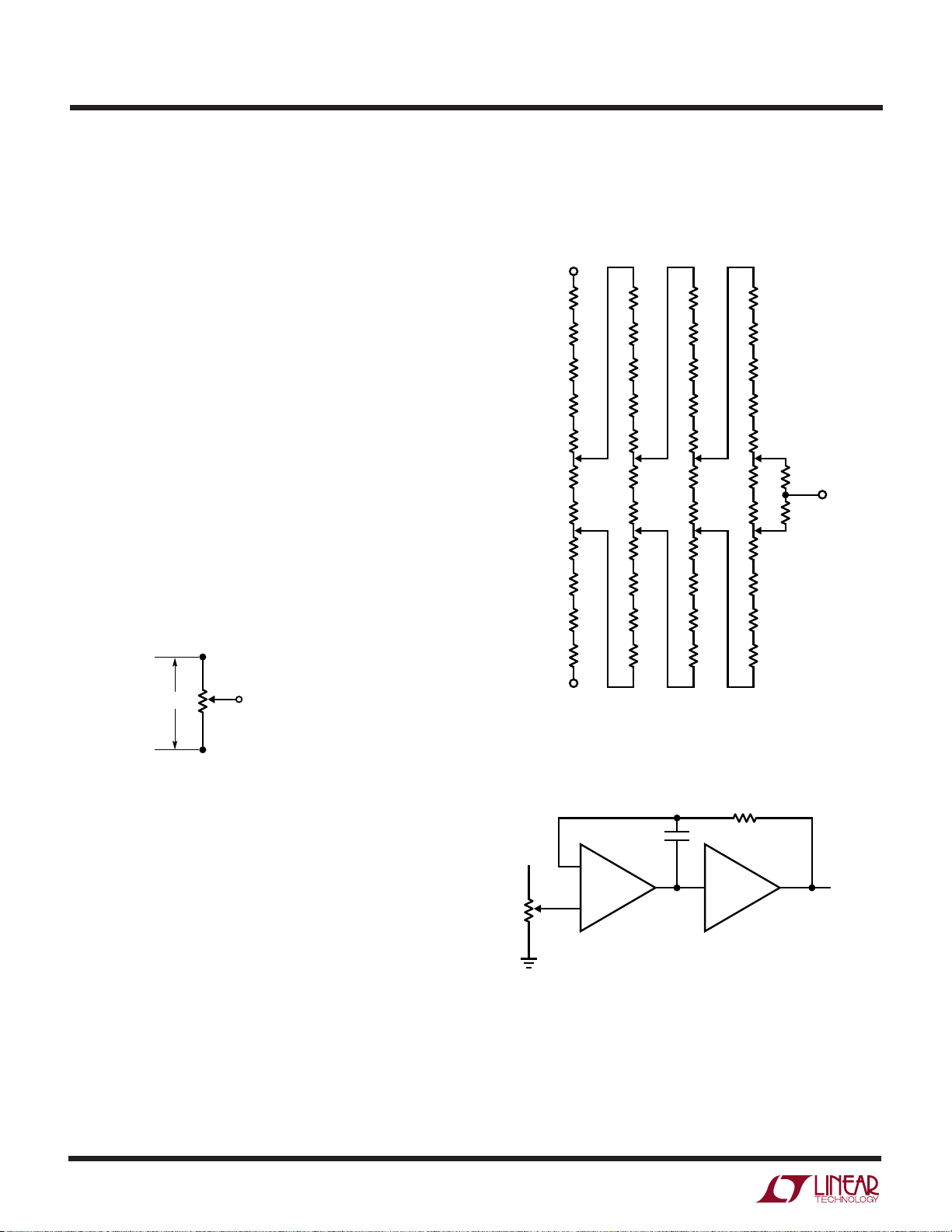
3-terminal potentiometer with fixed “end-to-end” resistance and a 7-decade switched wiper position (Figure C1).
SEVEN-DECADE SWITCHED
R = 100k
WIPER POSITION PERMITS
SETTING TO 0.1ppm LINEARITY
AN86 FC01
10k 2k 400Ω 80Ω
INPUT
80Ω
OUT
80Ω
COMMON
Figure C2. A 4-Decade Kelvin-Varley Divider. Additional
Decades Are Implemented By Opening Last Switch, Deleting
Two Associated 80Ω Values and Continuing ÷ 5 Resistor Chains
AN86 FC02
Figure C1. Conceptual Kelvin-Varley Divider
The actual construction of a 0.1ppm KVD is more artistry
and witchcraft than science. The market is relatively small,
the number of vendors few and resultant price high. If
$13,000 for a bunch of switches and resistors seems
offensive, try building and certifying your own KVD. Figure
C2 shows a detailed schematic.
The KVD shown has a 100kΩ input impedance. A consequence of this is that wiper output resistance is high and
varies with setting. As such, a very low bias current
follower is required to unload the KVD without introducing
significant error. Now, our KVD looks like Figure␣ C3. The
LT1010 output buffer allows driving cables and loads and,
more subtly, maintains the amplifier’s high open-loop
gain.
AN86-8
10k
0.1µF
E
INPUT
KVD
Figure C3. KVD with Buffer Gives Output Drive Capability
–
LT1010LTC1152
+
KVD = ELECTRO SCIENTIFIC INDUSTRIES RV-722,
FLUKE 720A OR JULIE RESEARCH LABS VDR-307
OUTPUT
AN86 FC03
Page 9
Application Note 86
Approach and Error Considerations
This schematic is deceptively simple. In practice, construction details are crucial. Parasitic thermocouples
(Seebeck effect), layout, grounding, shielding, guarding,
cable choice and other issues affect achievable performance.1 In fact, as good as the chopper-stabilized LTC1152
is with respect to drift, offset, bias current and CMRR,
selection is required if we seek sub-ppm nonlinearity
performance. Figure C4, an error budget analysis, details
some of the selection criteria.
10k
0.1µF
–
LTC1152
+
WORST-CASE
SPEC
5µV
0.05µV/°C
50pA
110dB
140dB
–
LTC1152
+
0.1µF
LT1010
REALISTIC SELECTION
TARGET
0.5µV
0.05µV/°C
10pA
140dB
140dB
10k
LT1010
FLOATING, BATTERY-POWERED
µV NULL DETECTOR
HP-419A
OUTPUT
ERROR IN
PPM
0.1
0.01/°C
0.1
0.1
0.1
AN86 FC04
OUTPUT
AN86 FC05
≈ 30k
OUTPUT
ERROR
SOURCE
E
OS
E
OS∆T
I
B
CMRR
5V
KVD RIN = 100k
WORST-CASE
RESISTANCE
FINITE GAIN
Figure C4. Error Budget Analysis for the KVD Buffer.
Selection Permits ≈0.4ppm Predicted Linearity Error
5V
KVD
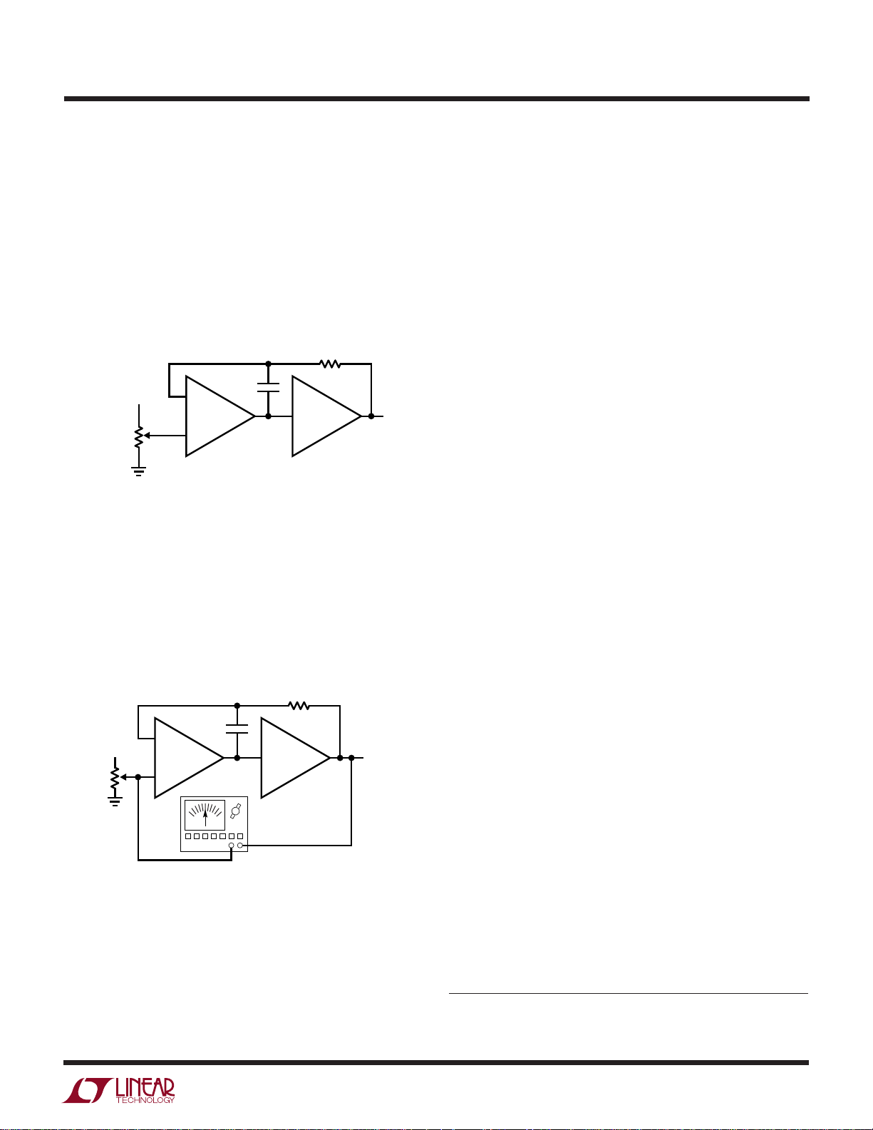
The buffer is tested with Figure C5’s circuit. As the KVD is
run through its entire range, the floating null detector must
remain well within 1ppm (5µV), preferably below 0.5ppm.
This test ensures that all error sources, particularly IB and
CMRR, whose effects vary with operating point, are accounted for. Measured performance indicates the sum of
all errors called out in Figure C4 is well within desired
limits.
In Figure C6, we add offset trim, a stable voltage source
and a second KVD to drive the main KVD. Additionally, an
ensemble of three HP3458A voltmeters monitor the output.
The offset trim bleeds a small current into the main KVD
ground return, producing a few microvolts of offset-trim
range. This functionally trims out all sources of zero error
(amplifier offsets, parasitic thermocouple mismatches
and the like), permitting a true zero volt output when the
main KVD is set to all zeros.
The voltmeters, specified for < 0.1ppm nonlinearity on the
10V range, “vote” on the source’s output.
Circuitry Details
Figure C7 is a more detailed schematic. It is similar to
Figure C6 but highlights issues and concerns. The grounding scheme is single point, preventing mixing of return
currents and the attendant errors. The shielded cables
used for interconnections between the KVDs and voltmeters should be specified for low thermal activity. Keithley
type SC-93 and Guildline #SCW are suitable. Crush type
copper lugs (as opposed to soldered types) provide lower
parasitic thermocouple activity at KVD and DVM connection points. However, they must be kept clean to prevent
oxidation, thus avoiding excessive thermal voltages.2 A
copper deoxidant (Caig Labs “Deoxit” D100L) is quite
effective for maintaining such cleanliness. Low thermal
lugs and jacks, preterminated to cables, are also available
(Hewlett-Packard 11053, 11174A) and convenient.
Figure C5. Determining Buffer Error By Measuring Input-Output
Deviation with Floating Microvolt Null Detector. Technique
Permits Evaluation of Fixed and Operating Point Induced Errors
Thermal baffles enclosing KVD and DVM connections tend
Note 1: See Appendix J, “Cables, Connections, Solder, Layout,
Component Choice, Terror and Arcana,” for relevant tutorial.
Note 2: See above Footnote.
AN86-9
Page 10
Application Note 86
to thermally equilibrate their associated banana jack terminals, minimizing residual parasitic thermocouple activity. Additionally, restrict the number of connections in the
signal path. Necessary connections should be matched in
number and material so that differential cancellation occurs. Complying with this guideline may necessitate deliberate introduction of solder-copper junctions (marked “X”
on Figure␣ C7) to obtain optimum differential cancellation.
3
This is normally facilitated by simply breaking the appropriate wire or PC trace and soldering it. Ensure that the
introduced thermocouples temperature track the junctions they are supposed to cancel. This is usually accomplished by locating all junctions within close physical
proximity.
The noise filtering capacitor at the main KVD is a low
leakage type, with its metal case driven by the output
buffer to guard out surface leakage.
When studying the approach used, it is essential to differentiate between linearity and absolute accuracy. This
eliminates concerns with absolute standards, permitting
certain freedoms in the measurement scheme. In particular, although single-point grounding was used, remote
sensing was not. This is a deliberate choice, made to
minimize the number of potential error-causing parasitic
thermocouples in the signal path. Similarly, a ratiometric
reference connection between the KVD LTZ1000A voltage
source and the voltmeters was not utilized for the same
reason. In theory, a ratiometric connection affords lower
drift. In practice, the resultant introduced parasitic thermocouples obviate the desired advantage. Additionally,
the aggregate stability of the LTZ1000A reference and the
voltmeter references (also, incidentally, LTZ1000A based)
is comfortably inside 0.1ppm for periods of 10 minutes.
4
This is more than enough time for a 10-point linearity
measurement.
STABLE
VOLTAGE
SOURCE
(LTZ1000A
BASED)
KVD
ADJUST FOR
5.000000V AT A
–
LTC1150
+
Figure C6. Simplified Sub-ppm Linearity Voltage Source
0.1µF
OFFSET
TRIM
+V
–V
10k
LT1010
20k
MAIN
KVD
A
R
WIRE
10k
0.1µF
–
LT1010LTC1152
+
HP3458A
HP3458A
HP3458A
OUTPUT
0.000000V
TO
5.000000V
AN86 FC06
AN86-10
Note 3: See Appendix J, “Cables, Connections, Solder, Layout,
Component Choice, Terror and Arcana,” for further discussion.
Note 4: The LTZ1000A reference is detailed in Appendix I, “ Voltage
References.”
Page 11
Application Note 86
Construction
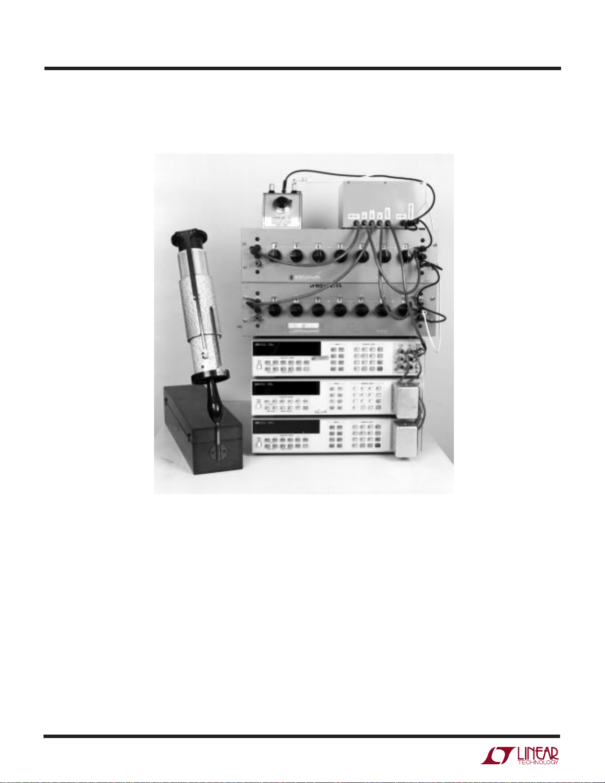
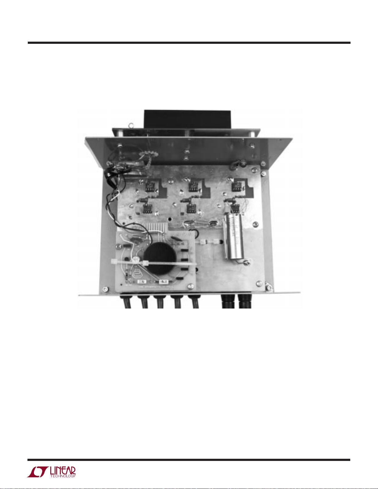
Figures C8 and C9 are photographs of the voltage source
and the reference-buffer box internal construction. The
figure captions annotate some significant features.
Results
This KVD-based, high linearity voltage source has been in
use in our lab for nearly two years. During this period, the
total linearity uncertainty defined by the source and its
monitoring voltmeters has been just 0.3ppm (see Figure
SEE APPENDIX F
FOR CIRCUIT DETAILS
OF LTZ1000A
ADJUST FOR
STABLE
VOLTAGE
SOURCE
(LTZ1000A
BASED)
KVD
5.000000V AT A
10k
0.1µF
–
LTC1150
+
OFFSET
TRIM
2k
+V
–V
10k
LT1010
20k
R
MAIN
KVD
WIRE
C10’s measurement regime). This is more than 3 times
better than the desired 1ppm performance, promoting
confidence in our measurements.
5
Acknowledgments
The author is indebted to Lord Kelvin and to Warren Little
of the C. S. Draper Laboratory (née M. I. T. Instrumentation
Laboratory) standards lab. Warren taught me, with great
patience, the wonders of KVDs some thirty years ago and
I am still trading on his efforts.
10k
A
–
10k
+
2µF
CASE
0.1µF
LT1010LTC1152
HP3458A
OUTPUT
0.000000V
TO
5.000000V
= SOLDER-COPPER JUNCTION.
PLACEMENT AND NUMBER AS REQUIRED
2µF = POLYSTYRENE. COMPONENT RSCH. CORP.
USE LOW THERMAL, LOW TRIBOELECTRIC
SHIELDED CABLE FOR KVD AND DVM CONNECTIONS.
SEE TEXT
Figure C7. Complete Sub-ppm Linearity Voltage Source
HP3458A
HP3458A
AN86 FC07
HIGH QUALITY
GROUND
Note 5: The author, wholly unenthralled by web surfing, has spent
many delightful hours “surfing the Kelvin.” This activity consists of
dialing various Kelvin-Varley divider settings and noting monitoring
A-to-D agreement within 1ppm. This is astonishingly nerdy behavior,
but thrills certain types.
AN86-11
Page 12
Application Note 86
AN86 FC08.tif
Figure C8. The Sub-ppm Linearity Voltage Source. Box Upper Right Is LTZ1000A Based Reference and Buffers. Upper Left Is Offset
Trim. Reference and Main Kelvin-Varley Dividers Are Photo Center—Upper and Center-Middle, Respectively. Three HP3458 DVMs
(Photo Lower) Monitor Output. Computer (Left Foreground) Aids Linearity Calculations
AN86-12
Page 13
Application Note 86
AN86 FC09.tif
Figure C9. Reference-Buffer Box Construction. LTZ1000A Reference Circuitry Is Photo Lower Left, Buffer Amplifiers Photo Center. Note
Capacitor Case Bootstrap Connection (Photo Center—Right). Single Point Ground Mecca Appears Photo Upper Left. Power Supply
(Photo Top) Mounts Outside Box, Minimizing Magnetic Field Disturbance
1. VERIFY KVD LINEARITY BY INTERCOMPARISON AND INDEPENDENT CAL. LAB.
2. TAKE WORST-CASE VOLTMETER ENSEMBLE DEVIATIONS OVER 0V TO 5V, EVERY 0.5V
3. 100 RUNS (10 PER DAY, ONCE PER HOUR)
4. INDICATED RESULT IS 0.3ppm NONLINEARITY
Figure C10. Testing Regime for the High Linearity Voltage Source
AN86 FC10
AN86-13
Page 14
Application Note 86
10k
10k
MCLR
2
3
4
5
6
7
8
9
11
1
10
D0
D1
D2
D3
D4
D5
D6
D7
CLK
OE
GND
19
18
17
16
15
14
13
12
20
Q0
Q1
Q2
Q3
Q4
Q5
Q6
Q7
V
CC
0.1µF
U2
74HCT574
2
3
4
5
6
7
8
9
11
1
10
D0
D1
D2
D3
D4
D5
D6
D7
CLK
OE
GND
19
18
17
16
15
14
13
12
20
Q0
Q1
Q2
Q3
Q4
Q5
Q6
Q7
V
CC
0.1µF
0.1µF
5V
4MHz
CRYSTAL
U3 74HCT574
2
3
4
5
6
7
8
9
11
1
10
D0
D1
D2
D3
D4
D5
D6
D7
CLK
OE
GND
19
18
17
16
15
14
13
12
20
Q0
Q1
Q2
Q3
Q4
Q5
Q6
Q7
V
CC
0.1µF
AN86 FD01
U4 74HCT574
1
2
3
4
5
6
7
8
9
10
11
12
13
14
USER INPUT
V
DD
NC
V
SS
NC
ADC SCK
ADC SDO
NC
NC
LSB OE
MID OE
MSB OE
LSB WR
MSB WR
28
27
26
25
24
23
22
21
20
19
18
17
16
15
10k
10k
10k
10k
10k
10k
10k
10k
MCLR
CLKIN
CLKIN2
MSB D7
D6
D5
D4
D3
D2
D1
LSB D0
DAC RDY
DAC LD
MLBYTE
D7 MSB
D6
D5
D4
D3
D2
D1
D0
5V
DAC
COMMANDS
TO ANALOG
SECTION
TO LTC2400
IN ANALOG
SECTION
U1 PIC16C5X
10k
10k
10k
10k
10k
10k
DAC LD
MLBYTE
MSB WR
LSB WR
ADC SDO
ADC SCK
20pF
20pF
USER
DATA
INPUT
MSB
DAC RDY
DAC WR
LSB
1ppm
5V
2ppm
5V
4ppm
5V
FILTER
5V
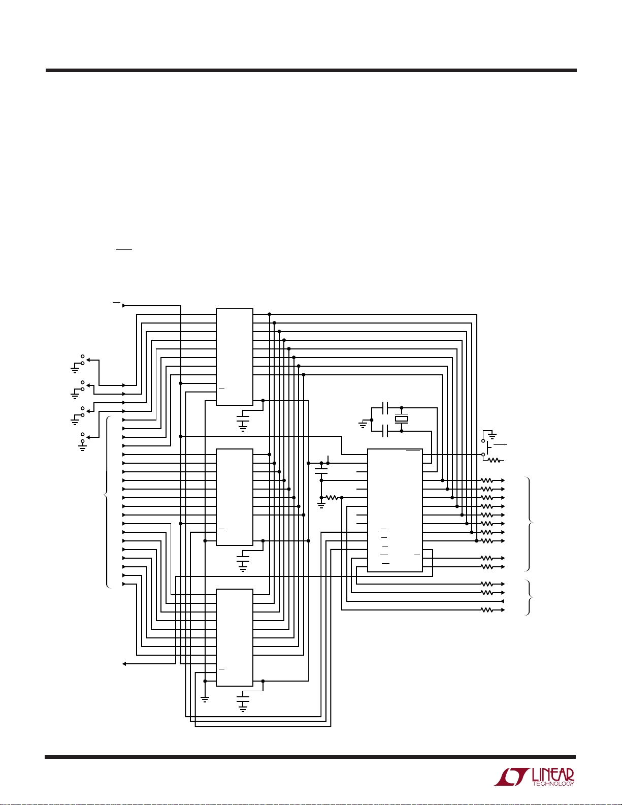
APPENDIX D
A PROCESSOR-BASED CODE COMPARATOR
The code comparator enforces the loop by setting the
slave DAC inputs to the code that equalizes the user input
and the LTC2400 A-to-D output. This action is more fully
described on page one of the text.
Figure D1 is the code comparator’s digital hardware. It is
composed of three input data latches and a PIC-16C5X
processor. Inputs include user data (e.g., DAC inputs),
linearity curvature correction (via DIP switches), convert
command (“DA WR”) and a selectable filter time constant.
An output (“DAC RDY”) indicates when the DAC output is
settled to the user input value. Additional outputs and an
AN86-14
Figure D1. Code Comparator Hardware. User Control Lines Are at Left, Analog Section Connections Appear at Right Side
input control and monitor the analog section (text Figure␣ 2) to effect loop closure. Note that although a total of
32 bits are presented to the two 16-bit slave DACs, there
are 8 bits of overlap, allowing a total dynamic range of 24
bits. This provides 4 bits of indexing range below the 20th
bit, ensuring a stable LSB of 1ppm of scale. The 8-bit
overlap assures the loop will always be able to capture the
correct output value.
The processor is driven by software code, authored by
Florin Oprescu, which is described below.
Page 15

Application Note 86
;20bit DAC code comparator
;
;***************************************************
; *
; Filename: dac20.asm *
; Date 12/4/2000 *
; File Version: 1.1 *
; *
; Author: Florin Oprescu *
; Company: Linear Technology Corp. *
; *
; *
;***************************************************
;
; Variables
;============
; uses 17 bytes of RAM as follows:
;
; {UB2, UB1, UB0} user input word buffer
;———————————————————————————————————————
; 24 bits unsigned integer (3 bytes):
;
; The information is transferred from the external input register
; into {UB2, UB1, UB0} whenever a “user input update” event
; is detected by testing the timer0 content. Following the data
; transfer, the UIU (“user input update”) flag is set and the DAC
; ready flags RDY and RDY2 are cleared. UB0 uses the same physical
; location as U0. The user input double buffering is necessary
; because the loop error corresponding to the current ADC reading
; must be calculated using the previous user input value.
; The old user input value can be replaced by the new user input
; value only after the loop error calculation.
; The worst case minimum response time to an UIU event must be
; calculated. The user shall not update the external input register
; at intervals shorter than this response time. For the moment the
; program can not block the user access to the external input
; register during a read operation. In such a situation the result
; of the read operation can be very wrong.
;
; UB0 - least significant byte. Same physical location as U0
;
; UB1 - second byte.
;
; UB2 - most significant byte.
;
;
; {U2, U1, U0} user input word
;——————————————————————————————
; 24 bits unsigned integer (3 bytes):
;
; The information is transferred from {UB2, UB1, UB0[7:4], [0000]}
; into {U2, U1, U0} whenever the UIU flag is found set within the
; CComp (“code comparator”) procedure. The UIU flag is reset
; following the data transfer.
AN86-15
Page 16

Application Note 86
;
; U0 - least significant byte of current DAC input
; The 4 least significant bits U0[3:0] are set
; to zero.
;
; U1 - second byte of current DAC input
;
; U2 - most significant byte of current DAC input
;
;
; {CON} control byte
;————————————————————
; (1 byte):
;
; The 3 least significant bits CON[2:0] represent the ADC linearity
; correction factor transferred from UB[2:0] when the UIU flag
; is found set within the CComp procedure - at the same time as the
; {U2, U1, U0} variable is updated.
;
; The effect of CON[2:0] is additive and its weight is as follows:
;
; CON[0] = 1 linearity correction effect is about 1ppm
; CON[1] = 1 linearity correction effect is about 2ppm
; CON[2] = 1 linearity correction effect is about 4ppm
;
; The LTC2400 has a typical 4ppm INL error therefore the default
; curvature correction value can be set at CON[2:0] = 100
;
; CON[3] is the control loop integration factor transferred from
; UB[3] when the UIU flag is found set within the CComp procedure.
; If CON[3]=0, after the control loop error becomes less than 4ppm
; the error correction gain is reduced from 1 to 1/4
; If CON[3]=1, after the control loop error becomes less than 4ppm
; the error correction gain is reduced from 1 to 1/16
;
; CON[7] is used as the UIU (“user input update”) flag. It is set
; when {UB2, UB1, UB0} is updated and it is reset when {U2, U1, U0}
; and CON[3:0] are updated.
;
; CON[6] is used as the RDY (“DAC ready”) flag. It is set when
; the DAC loop error becomes less than 4ppm and it is reset when
; the UIU flag is set.
;
; CON[5] is used as the RDY2 (“DAC ready twice”) flag. It is set
; whenever the DAC loop error becomes less than 4ppm and the RDY
; flag has been previously set. It is reset when the UIU flag is set.
;
;
; The bit CON[4] is not used and is always set to 0.
;
;
AN86-16
Page 17

Application Note 86
; {ADC3, ADC2, ADC1, ADC0} formatted ADC conversion result
;—————————————————————————————————————————————————————————
; 32 bits signed integer (4 bytes).
;
; The ADC reading is necessary only for the calculation of the control
; loop error and in order to save RAM space, it can share the same
; physical space as the loop error variable.
;
; The LTC2400 output format is offset binary. It must be converted
; to 2’s complement before any arithmetic operation. A number of
; possible codes are not valid LTC2400 output codes. If such codes
; are detected it can be inferred that a serial transfer error has
; occurred, the data must be discarded and a new conversion must
; be started. For all LTC2400 devices B31=0 and B30=0 always. In
; addition, with the exception of some early samples of the device
; the sequence B[29:28]=00 should not occur in a valid transaction.
;
; ADC0 - least significant byte
; contains ADC output bits B11(MSBIT) to B4 (LSBIT)
;
; ADC1 - second byte
; contains ADC output bits B19(MSBIT) to B12 (LSBIT)
;
; ADC2 - third byte
; contains ADC output bits B27(MSBIT) to B20 (LSBIT)
;
; ADC3 - most significant byte
; contains ADC output bits ~B29(as 7 MSBITS for
; 2’s complement sign extension) and B28 (LSBIT)
;
;
; {ADCC} ADC curvature correction
;————————————————————————————————
; 8 bits unsigned integer (1 byte)
;
; The LTC2400 transfer characteristic has a typical INL of about
; 4ppm and a parabolic shape symmetric with respect to mid-scale.
; This error can be corrected to a first and second order and
; ADDC contains the magnitude of this correction.
;
;
; {ER3, ER2, ER1, ER0} control loop error value
;——————————————————————————————————————————————
; signed integer (4 bytes)
;
; Contains the value of the current control loop error calculated
; as the difference between the previous user input and the last
; ADC reading. It is used to adjust the Low_DAC setting. Uses the
; same physical location as {ADC3, ADC2, ADC1, ADC0}:
;
; ER0 - least significant byte, same location as ADC0
;
; ER1 - second byte, same location as ADC1
AN86-17
Page 18

Application Note 86
;
; ER2 - third byte, same location as ADC2
;
; ER3 - most significant byte, same location as ADC3
;
;
; {DL3, DL2, DL1, DL0} Low DAC control value
;———————————————————————————————————————————
; signed integer (4 bytes):
;
; Contains the Low_DAC setting in a 2’s complement, 32 bit
; format. Must be initialized to 0!
;
; DL0 - least significant byte - used for Low_DAC
; control
;
; DL1 - second byte - used for Low_DAC control after
; conversion to offset binary format {DL1, DL0}
;
; DL2 - third byte - may be only 00 or FF
;
; DL3 - most significant byte - may be only 00 or FF
;
;
; {INDX} Index variable for various program functions
;————————————————————————————————————————————————————
; 1 byte.
;
;
; {TMPV} Temporary variable for various program functions
;————————————————————————————————————————————————————————
; 1 byte.
;
;
;
; Algorithm
;===========
;
; After each ADC conversion cycle the processor calculates the control
; loop error value as the difference between the desired output and
; the latest conversion result. Than it updates the DACs command
; such as to reduce the error magnitude. A new ADC conversion cycle
; is started following the DACs update operation.
;
; In order to maintain adequate control loop stability it is necessary
; for the DACs and the associated amplifiers to settle to better than
; 20 bits accuracy before the ADC starts sampling the system output. For
; an LTC2400 based system this settling time is 66ms.
;
; Initialization:
; Initializes the PIC controller and the hardware interface
; and starts the Scan procedure.
;
AN86-18
Page 19

Application Note 86
; 1. Load ADC control port with default values
; SCKAD = 0
; SDOAD = 1
; 2. Set ADC control port I and O pins
; SCKAD = output
; SDOAD = input
; 3. Load register control port with default values
; NCSR[2:0] = 111
; NCSD[1:0] = 11
; ADDAC = 1
; NLDAC = 1
; DACRDY = 0
; 4. Set register control port in output mode
; 5. Set data bus to default value DBUS[7:0]=0x00
; 6. Set data bus in output mode
; 7. Initialize internal registers and variables:
; OPTION = 0x2F
; Timer0 used as counter is incremented by low-to-high edge
; Prescaler works with watch dog timer in div128 mode
; CON = 0x80
; Simulate a UIU “user interface update” event to force
; the update of both Low_DAC and High_DAC
; {DL3, DL2, DL1, DL0} = 0
; { U2, U1, U0} = 0
; 8. Update hardware using the initialized variables
; 9. Start new ADC conversion by reading and discarding
; 32 serial bits.
; 10.Start the Scan procedure
;
; Scan:
; Continuously looks for “user input update” events. When
; a “user input update” event is detected updates the
; input buffer {UB2, UB1, UB0}, resets timer, sets UIU flag
; and resets RDY and RDY2 flags.
;
; The active low write signal for the external input register
; (which is the same as the user interface NWR input signal)
; is driven by the user and it is connected to the counter
; input of Timer0. The Timer0 is used in counter mode without a
; prescaler and it increments whenever a low-to-high transition
; is detected at its input. This is the same transition which
; latches in the input register a new user command.
; Because of the PIC controller timing constraints, this write
; signal must be maintained low for at least 2*Tosc + 20ns
; where Tosc is the maximum PIC clock period. When a 4 MHz
; clock is used for the PIC processor, the low time must be
; longer than about 520ns.
;
; 1. Test for “user input update” events by testing the Timer0
; value.
; If Timer0>0 an UIU event has occurred. Reset the timer
; and answer Yes.
; If Timer0=0 answer No.
AN86-19
Page 20

Application Note 86
; 1.1 If Yes, read input latch into {UB2, UB1, UB0},
; reset DACRDY output line, set UIU flag and
; and reset RDY and RDY2 flags (CON[7:5]=100)
; Than continue
; 1.2 If No continue
;
; Continuously looks for the ADC end of conversion event. When
; the “end of conversion” is detected it reads the 28 most
; significant bits from the ADC and it constructs the ADC
; result {ADC3, ADC2, ADC1, ADC0} in 2’s complement format
; If ADC3[1] == 0 => ADC3[7:1]=1111 111
; If ADC3[1] == 1 => ADC3[7:1]=0000 000
; For very early LTC2400 samples only, it is possible
; to obtain as a valid 0 conversion result ADC3[1:0]=00
; In this case:
; If ADC3[1:0] == 0 => ADC3=0
; It also calculates the first (x1) and second (x2) order ADC
; curvature correction ADCC as follows:
; x1 = {0x00, 0x80} ; -abs({ADC3, ADC2, ADC1, ADC0}/(2^16)-{0x00, 0x80})
; x2 = {0x00, 0x40} ; -abs({0x00,{0,ADC2[6:0]},ADC1,ADC0}/(2^16)-{0x00,0x40})
; ADCC = floor((x1 + x2/2) * {00000 CON[2:0]} / 4 )
; The actual implementation uses only the least significant
; byte of x without any substantial additional error.
; Thus the above relation can be modified as follows:
; ADCC = floor((abs(ADC2) + abs({ADC2[6],ADC2[6:0]})/2) *
; * {00000 CON[2:0]} / 4 )
; The maximum correction range is about 7ppm INL at mid
; scale for CON[2:0] = 111.
;
; 2. Test for ADC “end of conversion” event by testing the
; value of the ADC_SDO signal.
; If ADC_SDO = LOW answer Yes.
; If ADC_SDO = HIGH answer No.
; 2.1 If Yes read 28 most significant bits from the ADC,
; update {ADC3, ADC2, ADC1, ADC0} and calculate the
; curvature correction byte ADCC. Than start the CComp
; procedure.
; It should be noticed that while reading the first 28
; most significant bits from the ADC the controller
; generates 27 serial clock pulses. An additional 5 serial
; clock pulses (for a total of 32) are necessary to restart
; the conversion.
; 2.2 If No restart the Scan procedure.
;
;
; CComp:
; Calculates the current control loop error as:
;
; error = current_user_input - ADC_reading +
; + new_user_input_LSB - current_user_input_LSB
;
AN86-20
Page 21

Application Note 86
; The curvature correction is included in the ADC
; conversion result and is always positive therefore:
;
; ADC_reading = {ADC3, ADC2, ADC1, ADC0} +
; + { 0, 0, 0, ADCC}
;
; The term “new_user_input_LSB - current_user_input_LSB”
; represents the residue of the new user command which
; is added to the Low_DAC.
;
; {ER3, ER2, ER1, ER0} =
; = {0, U2, U1, U0} - {ADC3, ADC2, ADC1, ADC0} ; - { 0, 0, 0, ADCC} +
; + {0, 0, 0, UB0} - { 0, 0, 0, U0} =
;
; = {0, U2, U1, UB0} - {ADC3, ADC2, ADC1, ADC0} ; - { 0, 0, 0, ADCC}.
;
; The loop error {ER3, ER2, ER1, ER0} is a 32 bit signed number
; and the weight of the least significant bit is 1/16ppm of
; the ADC reference voltage. A 4ppm error value is represented
; as {0, 0, 0, 0x40}.
;
; The ADC output noise is dominated by thermal noise and has a
; white distribution. The control loop noise can be reduced by
; the square root of N by averaging N successive ADC readings.
; The obvious penalty is a slow settling time. Due to the
; limited amount of RAM available a direct implementation
; of this noise reduction strategy is difficult. In an equivalent
; implementation, when the absolute value of the loop error
; {ER3, ER2, ER1, ER0} decreases below a certain threshold, the
; gain of the error correction loop can be decreased. The default
; threshold is set at a very conservative 4ppm. This value must
; always be larger than the peak noise level of the ADC. A very
; quiet implementation can probably operate with a threshold of
; 2ppm. If CON[3]=0 the gain of the error correction loop is
; decreased from 1 to 1/4. If CON[3]=1 the gain of the error
; correction loop is decreased from 1 to 1/16.
;
; The High_DAC is always controlled by the 16 most significant
; bits of the most recent user command {UB2, UB1}
;
; The Low_DAC is controlled by the {DL3, DL2, DL1, DL0}
; variable which integrates the control loop error. Under
; correct operating condition abs({DL3, DL2, DL1, DL0})<2^15.
; In order to avoid roll-overs during large transients the
; {DL3, DL2, DL1, DL0} must be clamped within the +/- 2^15 range.
; The 16 bit Low_DAC can than be controlled by {DL1, DL0}
; after conversion to offset binary format.
;
AN86-21
Page 22

Application Note 86
; The DACRDY output line reflects the state of the
; internal RDY2 flag.
;
; After the updates are completed we must start a new ADC
; conversion by completing the serial transfer.
;
; 1. Test if UIU flag is set
; 1.1 If Yes, move UB[3:0] into CON[3:0]
; and {UB0[7:4], 0000} into U0. The last ADC result
; is curvature corrected using the previous CON[3:0] value!.
; 2. Calculate {ER3, ER2, ER1, ER0}.
; 3. Test if UIU flag is set
; 3.1 If Yes, move {UB2, UB1} into {U2, U1} and
; clear UIU, RDY and RDY2 flags (CON[7:5]=000 )
; 3.2 If No, test if abs({ER3, ER2, ER1, ER0}) < 4ppm
; 3.2.1 If Yes, test if CON[6]=1 (RDY flag)
; 3.2.1.1 If Yes, set RDY2 flag (CON[5]=1 )
; 3.2.1.2 If No, set RDY flag (CON[6]=1 )
; and test if CON[3]=0 (filter flag)
; 3.2.1.3 If Yes, {ER3, ER2, ER1, ER0} =
; = {ER3, ER2, ER1, ER0}/4
; 3.2.1.4 If No, {ER3, ER2, ER1, ER0} =
; = {ER3, ER2, ER1, ER0}/16
; 3.2.2 If No, clear UIU, RDY and RDY2
; flags (CON[7:5]=000 )
; 4 {DL3, DL2, DL1, DL0} = {DL3, DL2, DL1, DL0} +
; +{ER3, ER2, ER1, ER0}.
; 5. Update High_DAC, Low_DAC and DACRDY output line
; 6. Read the 4 least significant bits from ADC and start
; a new conversion
; 7. Restart the Scan procedure
;
;
; Hardware resources
;====================
;
; Uses 8 input/output pins, 9 output pins, 1 input pin and 1
; counter input pin
;
; DBUS[7:0] data bus
;———————————————————
; 8 bit bi-directional data bus is used to read the 20 bit input
; command IC[19:0], the one bit filter selection FS[0] and the 3 bit
; curvature correction selection CC[2:0]. It is also used to write
; the 16 bit Low_DAC command LDAC[15:0] and the 16 bit High_DAC
; command HDAC[15:0].
;
; assigned to PIC port C[7:0]
;
AN86-22
Page 23

Application Note 86
; The data format for the read and write operations is as follows:
;
; DBUS[ 7:0] = IC[19:12] when NCSR[2] = 0
; DBUS[ 7:0] = IC[11: 4] when NCSR[1] = 0
; DBUS[ 7:0] = {IC[3:0], FS[0], CC[2:0]} when NCSR[0] = 0
; LDAC[ 7:0] = DBUS[7:0] when NCSD[0] = 0 and ADDAC = 0
; LDAC[15:8] = DBUS[7:0] when NCSD[0] = 0 and ADDAC = 1
; HDAC[ 7:0] = DBUS[7:0] when NCSD[1] = 0 and ADDAC = 0
; HDAC[15:7] = DBUS[7:0] when NCSD[1] = 0 and ADDAC = 1
;
;
; NCSR[2:0] active low output enable controls for input registers
;————————————————————————————————————————————————————————————————
; 3 output lines used to selectively enable the three 8-bit input
; registers in order to read the user updated DAC command, the 3
; curvature correction bits and the one filter control bit.
;
; NCSR[0] enables the low input byte (LSB) and is assigned to port B[0]
;
; NCSR[1] enables the second input byte and is assigned to port B[1]
;
; NCSR[2] enables the high input byte (MSB) and is assigned to port B[2]
;
;
; NCSD[1:0] active low input enable controls for the DACs
;————————————————————————————————————————————————————————
; 2 output lines used to selectively enable the two DACs
;
; NCSD[0] enables the Low_DAC and is assigned to port B[3]
;
; NCSD[1] enables the High_DAC and is assigned to port B[4]
;
;
; ADDAC DAC address control
;——————————————————————————
; output line. A low enables a write operation to the low byte of
; Low_DAC or High_DAC. A high enables a write operation to the high
; byte of Low_DAC or High_DAC.
;
; ADDAC is assigned to port B[5]
;
;
AN86-23
Page 24

Application Note 86
; NLDAC active low DAC load control
;——————————————————————————————————
; output line. A high to low transition on this line updates the
; Low_DAC and High_DAC output values
;
; NLDAC is assigned to port B[6]
;
;
; DACRDY active high ready output signal
;———————————————————————————————————————
; output line. Indicates that the control loop error has been
; within a +/- 4ppm range for at least 250 ms
;
; DACRDY is assigned to port B[7]
;
;
; SCKAD external serial clock line for the ADC
;—————————————————————————————————————————————
; output line. ADC external serial clock. An external 10Kohm
; pull-down resistor is necessary on this line for correct
; power-up configuration.
;
; SCKAD is assigned to port A[0]
;
;
; SDOAD serial data line from ADC
;————————————————————————————————
; input line. Used to read ADC serial data.
;
; SDOAD is assigned to port A[1]
;
;
;
; NWRUI active low user interface write control
;——————————————————————————————————————————————
; input line. The user must bring this line low in order to update
; the DAC input value. A minimum low and high time is required !
;
; NWRUI is assigned to TOCKI counter input pin
;
;
;
AN86-24
Page 25

Application Note 86
; The spare I/O pins A[3:2] are configured as outputs and maintained LOW.
;
;;;;;;;;;;;;;;;;;;;;;;;;;;;;;;;;;;;;;;;;;;;;;;;;;;;;;;;;;;;;;;;;;;
list p=16c55A ; list directive to define processor
#include <p16c5x.inc> ; processor specific variable definitions
__CONFIG _CP_OFF & _WDT_ON & _XT_OSC
;VARIABLE DEFINITIONS
;====================
UB0 EQU H’0008' ; user input word buffer LSB
UB1 EQU H’0009' ; user input word buffer second byte
UB2 EQU H’000A’ ; user input word buffer MSB
U0 EQU H’0008' ; user input word LSB
U1 EQU H’000B’ ; user input word second byte
U2 EQU H’000C’ ; user input word MSB
CON EQU H’000D’ ; control byte
ADC0 EQU H’000E’ ; ADC conversion result LSB
ADC1 EQU H’000F’ ; ADC conversion result second byte
ADC2 EQU H’0010' ; ADC conversion result third byte
ADC3 EQU H’0011' ; ADC conversion result MSB
ADCC EQU H’0012' ; ADC curvature correction byte
ER0 EQU H’000E’ ; control loop error LSB
ER1 EQU H’000F’ ; control loop error second byte
ER2 EQU H’0010' ; control loop error third byte
ER3 EQU H’0011' ; control loop error MSB
DL0 EQU H’0013' ; Low_DAC LSB
DL1 EQU H’0014' ; Low_DAC second byte
DL2 EQU H’0015' ; Low_DAC third byte
DL3 EQU H’0016' ; Low_DAC MSB
INDX EQU H’0017' ; index variable
TMPV EQU H’0018' ; temporary variable
#define OPRDF 0x2F ; OPTION register default value
#define CONDF 0x80 ; CON register default value
AN86-25
Page 26

Application Note 86
;HARDWARE ASSIGNMENT DEFINITIONS
;===============================
#define DBUS PORTC ; 8bit I/O data bus
#define REGCN PORTB ; register control port
#define REGDF 0x7F ; register control port default value
#define NCSR0 PORTB,0 ; LSB input register active low output enable
#define NCSR1 PORTB,1 ; second byte input register active low output enable
#define NCSR2 PORTB,2 ; MSB input register active low output enable
#define NCSD0 PORTB,3 ; Low_DAC active low write enable
#define NCSD1 PORTB,4 ; High_DAC active low write enable
#define ADDAC PORTB,5 ; address bit for Low_DAC and High_DAC
#define NLDAC PORTB,6 ; active low load control for Low_DAC and High_DAC
#define DACRDY PORTB,7 ; 20bit_DAC ready indicator
#define ADCCN PORTA ; ADC control port
#define ADCTR 0x02 ; ADC control port configuration
; SDOAD input, the rest outputs
#define ADCDF 0x02 ; ADC control port default value
#define SCKAD PORTA,0 ; ADC external serial clock
#define SDOAD PORTA,1 ; ADC serial data output
;THE CODE
;===============================
RESET ORG 0x1FF ; processor reset vector
goto start
ORG 0x000
;Initialization procedure
;————————————————————————
start movlw ADCDF ;write ADC control port default value
movwf ADCCN ;
movlw ADCTR ;set the I and O pin states for the
tris ADCCN ;ADC control port
;
movlw REGDF ;write register control port default value
movwf REGCN ;
clrw ;set register control port pins as
tris REGCN ;output only
;
movwf DBUS ;set DBUS default value of 0
tris DBUS ;set DBUS as output
;
movlw OPRDF ;set OPTION register default value
option ;
;
AN86-26
Page 27

Application Note 86
clrf TMR0 ;
btfss STATUS,NOT_TO ;if this is not a power-on reset
movwf TMR0 ;load Timer0 with a nonzero value
;to force an initial read of the
;external input register
;
clrf DL3 ;initialize {DL3, DL2, DL1, DL0}=0
clrf DL2 ;
clrf DL1 ;
clrf DL0 ;
clrf U2 ;initialize {U2, U1, U0}=0
clrf U1 ;
clrf U0 ;
;
movlw CONDF ;set CON variable default value
movwf CON ;
;prepare to trigger a new ADC conversion
;after completing a hardware update
movlw 0x20 ;read and discard 32 serial bits from
movwf INDX ;the ADC
;
goto iupdt ;go to the hardware update function
;ADC output buffer flush function
;————————————————————————————————
fladc movlw 0x20 ;reads and discards 32 serial bits from
movwf INDX ;the ADC
;ADC dummy serial read function
;——————————————————————————————
;reads and discards the number of serial
;bits indicated by the INDX variable
rddmy bsf SCKAD ;low-to-high ADC serial clock edge
bcf SCKAD ;high-to-low ADC serial clock edge
decfsz INDX,1 ;test if we read enough bits
goto rddmy ;if No, read one more bit
btfss SDOAD ;if Yes test that a new conversion has started
goto fladc ;if No, there is an interface problem. Flush the
;ADC output buffer and start a new conversion
goto scan ;if Yes restart the scan procedure
;external input register read function
;—————————————————————————————————————
rduiu movlw 0xFF ;input register read routine
tris DBUS ;set data bus in read mode (input)
bcf NCSR0 ;output enable for input reg. LSB
nop ;wait for data bus to settle
movf DBUS,0 ;read input reg. LSB
bsf NCSR0 ;output disable for input reg. LSB
bcf NCSR1 ;output enable for input reg. second byte
movwf UB0 ;store input reg. LSB into input buffer
movf DBUS,0 ;read input reg. second byte
bsf NCSR1 ;output disable for input reg. second byte
AN86-27
Page 28

Application Note 86
bcf NCSR2 ;output enable for input reg. MSB
movwf UB1 ;store input reg. second byte into input buffer
movf DBUS,0 ;read input reg. MSB
movwf UB2 ;store input reg. MSB into input buffer
clrw ;terminate input reg. read operation
bsf NCSR2 ;output disable for input reg. MSB
tris DBUS ;return data bus to write mode
clrf TMR0 ;clear Timer0 to continue wait for a UIU event
bcf DACRDY ;signal user that input data has been read
bsf CON,7 ;set UIU flag
bcf CON,6 ;clear RDY flag
bcf CON,5 ;clear RDY2 flag
;scan procedure
;——————————————
;monitors UIU and end-of-conversion events
scan movf TMR0,1 ;test if Timer0 = 0
btfss STATUS,Z ;if Timer0=0 no UIU has occurred, skip next
goto rduiu ;a user interface update has occurred
;go and read the new DAC input data
btfsc SDOAD ;test ADC end of conversion signal
goto scan ;conversion not ready, rescan
;ADC serial read function
;————————————————————————
rdadc movlw 0x1B ;ADC conversion is done, read first 28 bits
movwf INDX ;the first bit must be “0” to get here
;so do not bother with it
rdbit bsf SCKAD ;low-to-high ADC serial clock edge
bcf SCKAD ;high-to-low ADC serial clock edge
bcf STATUS,C ;move ADC output bit to carry. First clear carry
btfsc SDOAD ;read ADC output bit
bsf STATUS,C ;if ADC output is “1” set carry
rlf ADC0,1 ;load carry as msb of ADC result
rlf ADC1,1 ;and shift left all 4 bytes of the ADC result
rlf ADC2,1 ;
rlf ADC3,1 ;
decfsz INDX,1 ;test if all 28 bits have been read
goto rdbit ;if not, continue
;
;we have skipped the first ADC bit (ADC bit31=0)
;which has been tested as =0 when we detected the
;end of conversion.
;we have read 27 additional bits and have generated
;27 clock pulses. To restart the conversion we must
;produce the 5 remaining clock pulses
AN86-28
Page 29

Application Note 86
;verify validity of ADC serial data and format it
;————————————————————————————————————————————————
btfsc ADC3,2 ;test if the ADC bit30 is “0”
goto fladc ;if not there is an interface problem. Flush the
;ADC output buffer and start a new conversion
;if yes, put the ADC result in 2’s complement form
movlw 0x03 ;first clear the 6 most significant bits in ADC3
andwf ADC3,1 ;
btfsc STATUS,Z ;tests for the [ADC_B29,ADC_B28]=00 ADC output
goto rdend ;if Yes the formatting is completed.
;in very early LTC2400 samples the ADC output code
;[ADC_B29,ADC_B28]=00 is valid
; goto fladc ;for current LTC2400 devices improved error
;detection capability is obtained if the
;previous line is replaced with this line.
;The replacement is not mandatory.
;For current LTC2400 parts the output code
;[ADC_B29,ADC_B28]=00 is not valid thus it may
;be assumed that an ADC interface error has
;occurred. Flush the ADC output buffer and start
;a new conversion
movlw 0x02 ;if No, convert ADC3 in 2’s complement form
btfss ADC3,1 ;
movlw 0xFE ;
xorwf ADC3,1 ;
;curvature correction calculator
;———————————————————————————————
;first order curvature correction multiplier
;use ADC2[7:0] as a 2’s complement number
rdend movf ADC2,0 ;calculate abs(ADC2)
btfsc ADC2,7 ;if ADC2[7]=0 w = ADC2
comf ADC2,0 ;else w = !ADC2
movwf ADCC ;ADCC=w=abs(ADC2)
;second order curvature correction multiplier
;use ADC2[6:0] as a 2’s complement number
movf ADC2,0 ;calculate abs(ADC2[6:0])
btfsc ADC2,6 ;if ADC2[6]=0 w = ADC2
comf ADC2,0 ;else w = !ADC2
movwf TMPV ;TMPV=w=abs(ADC2[6:0])
rrf TMPV,0 ;w=TMPV/2 in order to scale the second order
;curvature correction
andlw 0x1f ;clear 3 MSB of w to complete calculation
addwf ADCC,0 ;w=abs(ADC2)+abs(ADC2[6:0])/2
movwf TMPV ;TMPV contains the curvature correction multiplier
;
clrf ADCC ;
bcf STATUS,C ;clear carry for div-by-2 operation
btfsc CON,2 ;if CON[2]=1
AN86-29
Page 30

Application Note 86
movwf ADCC ;ADCC=ADCC+abs(ADC2)
rrf TMPV,1 ;TMPV=TMPV/2
movf TMPV,0 ;
bcf STATUS,C ;clear carry for div-by-2 operation
btfsc CON,1 ;if CON[1]=1
addwf ADCC,1 ;ADCC=ADCC+abs(ADC2)/2
rrf TMPV,1 ;TMPV=TMPV/2
movf TMPV,0 ;
btfsc CON,0 ;if CON[0]=1
addwf ADCC,1 ;ADCC=ADCC+abs(ADC2)/4
;code comparator procedure
;—————————————————————————
ccomp btfss CON,7 ;if the UIU flag is clear
goto ercalc ;skip CON[3:0] and U0 update
movlw 0xF0 ;else update CON[3:0]
andwf CON,1 ;clear CON[3:0]
movlw 0x0F ;extract new CON[3:0]
andwf UB0,0 ;from input buffer
iorwf CON,1 ;and load it
movlw 0xF0 ;move UB[7:4] to U0[7:4]
andwf UB0,1 ;UB0 and U0 use the same
;physical location
;calculate control loop error
;————————————————————————————
ercalc comf ADCC,1 ;ADCC 1’s complement
comf ADC0,1 ;ADC0 1’s complement
movlw 0x02 ;add carry-in for ADCC and for ADC0
;2’s complement conversion
clrf TMPV ;prepare carry-out accumulator
addwf UB0,0 ;w=carry-in + UB0
btfsc STATUS,C ;if there is a carry-out
incf TMPV,1 ;accumulate it
addwf ADCC,0 ;w=carry-in + UB0 - ADCC
btfsc STATUS,C ;if there is a carry-out
incf TMPV,1 ;accumulate it
addwf ADC0,1 ;ER0=UB0 - ADC0 - ADCC
;has same location as ADC0
btfsc STATUS,C ;if there is a carry-out
incf TMPV,1 ;accumulate it
AN86-30
Page 31

Application Note 86
comf ADC1,1 ;ADC1 1’s complement
movlw 0xff ;w=0xff (1’s complement of ADCC second byte)
addwf TMPV,0 ;w=0xff + carry-in
clrf TMPV ;prepare carry-out accumulator
btfsc STATUS,C ;if there is a carry-out
incf TMPV,1 ;accumulate it
addwf U1,0 ;w=0xff + carry-in + UB1
btfsc STATUS,C ;if there is a carry-out
incf TMPV,1 ;accumulate it
addwf ADC1,1 ;ER1=U1 - ADC1 - 0 + carry-in
;has same location as ADC1
btfsc STATUS,C ;if there is a carry-out
incf TMPV,1 ;accumulate it
comf ADC2,1 ;ADC2 1’s complement
movlw 0xff ;w=0xff (1’s complement of ADCC third byte)
addwf TMPV,0 ;w=0xff + carry-in
clrf TMPV ;prepare carry-out accumulator
btfsc STATUS,C ;if there is a carry-out
incf TMPV,1 ;accumulate it
addwf U2,0 ;w=0xff + carry-in + UB2
btfsc STATUS,C ;if there is a carry-out
incf TMPV,1 ;accumulate it
addwf ADC2,1 ;ER2=U2 - ADC2 - 0 + carry-in
;has same location as ADC2
btfsc STATUS,C ;if there is a carry-out
incf TMPV,1 ;accumulate it
comf ADC3,1 ;ADC3 1’s complement
decf TMPV,1 ;ADCC 2’s complement term. The next
;carry-in is not useful - discard
movf TMPV,0 ;w=carry-in
addwf ADC3,1 ;ER3= 0 - ADC3 - 0 + carry-in
;has same location as ADC3
btfsc CON,7 ;test if the UIU flag is set
goto lduiu ;go to U1, U2 update
AN86-31
Page 32

Application Note 86
movf ER3,0 ;W = ER3
btfsc ER3,7 ;test if {ER3, ER2, ER1, ER0} < 0
comf ER3,0 ;if yes W = -ER3
btfss STATUS,Z ;test if W=0
goto nrdy ;if not absolute error >= 4ppm
movf ER2,0 ;W = ER2
btfsc ER3,7 ;test if {ER3, ER2, ER1, ER0} < 0
comf ER2,0 ;if yes W = -ER2
btfss STATUS,Z ;test if W=0
goto nrdy ;if not absolute error >= 4ppm
movf ER1,0 ;W = ER1
btfsc ER3,7 ;test if {ER3, ER2, ER1, ER0} < 0
comf ER1,0 ;if yes W = -ER1
btfss STATUS,Z ;test if W=0
goto nrdy ;if not absolute error >= 4ppm
;error comparator
;————————————————
;calculate absolute value of loop error and
;compare loop error magnitude with the 4ppm
;threshold
movf ER0,0 ;W = ER0
btfsc ER3,7 ;test if {ER3, ER2, ER1, ER0} < 0
comf ER0,0 ;if yes W = -ER0
andlw 0xC0 ;keep only W[7:6] which are bits >= 4ppm
btfss STATUS,Z ;test if W[7:6]=0
goto nrdy ;if not absolute error >= 4ppm
;if we are here the absolute loop error is
;less than 4 ppm. Set the flags and
;scale the loop error.
btfsc CON,6 ;test if RDY flag is already set
bsf CON,5 ;if Yes, set RDY2 flag
bsf CON,6 ;set RDY flag in any case
AN86-32
Page 33

;error scaling
;—————————————
;reduce error correction value for loop
;damping and ADC noise reduction
btfsc CON,3 ;test if CON[3]=0
goto div4 ;if Yes ER0=ER0/4
;if No ER0=ER0/16
rrf ER0,1 ;*1/2
rrf ER0,0 ;*1/2
andlw 0x3F ;clear 2 most significant bits
btfsc ER3,7 ;if {ER3, ER2, ER1, ER0} < 0
iorlw 0xC0 ;set 2 most significant bits
movwf ER0 ;ER0=ER0/4
div4 rrf ER0,1 ;*1/2
rrf ER0,0 ;*1/2
andlw 0x3F ;clear 2 most significant bits
btfsc ER3,7 ;if {ER3, ER2, ER1, ER0} < 0
iorlw 0xC0 ;set 2 most significant bits
movwf ER0 ;ER0=ER0/4
goto eracc ;go to error accumulator
;load latest user input
;——————————————————————
lduiu movf UB1,0 ;
movwf U1 ;U1=UB1
movf UB2,0 ;
movwf U2 ;U2=UB2
nrdy movlw 0x1F ;
andwf CON,1 ;clear UIU, RDY and RDY2 flags
Application Note 86
;error accumulator
;—————————————————
;adds the current loop error to the
;previous Low_DAC control value
;{DL3, DL2, DL1, DL0}={DL3, DL2, DL1, DL0}+
; +{ER3, ER2, ER1, ER0}
eracc movf ER0,0 ;the carry-in is 0
clrf TMPV ;clear carry-in accumulator
addwf DL0,1 ;DL0=DL0+ER0
btfsc STATUS,C ;if there is a carryout
incf TMPV,1 ;accumulate in carry-in
movf TMPV,0 ;load carry-in
clrf TMPV ;clear carry-in accumulator
addwf ER1,0 ;W=ER1+carry-in
btfsc STATUS,C ;if there is a carryout
incf TMPV,1 ;accumulate in carry-in
addwf DL1,1 ;DL1=DL1+ER1
btfsc STATUS,C ;if there is a carryout
incf TMPV,1 ;accumulate in carry-in
movf TMPV,0 ;load carry-in
clrf TMPV ;clear carry-in accumulator
addwf ER2,0 ;W=ER2+carry-in
AN86-33
Page 34

Application Note 86
btfsc STATUS,C ;if there is a carryout
incf TMPV,1 ;accumulate in carry-in
addwf DL2,1 ;DL2=DL2+ER2
btfsc STATUS,C ;if there is a carryout
incf TMPV,1 ;accumulate in carry-in
movf TMPV,0 ;load carry-in
addwf ER3,0 ;W=ER3+carry-in
addwf DL3,1 ;DL3=DL3+ER3
btfss STATUS,Z ;test if DL3=0
goto negpot ;if No, DL may be negative
movf DL2,1 ;
btfss STATUS,Z ;test if DL2=0
goto ovflow ;if No, DL >= 2^15, must truncate
btfsc DL1,7 ;test if DL1[7]=1
goto ovflow ;if No, DL >= 2^15, must truncate
goto updt ;if Yes we are done with DL range control
;Low_DAC control truncation
;——————————————————————————
;limits the {DL3, DL2, DL1, DL0} range to
; abs({DL3, DL2, DL1, DL0}) < 2^15 by
;truncation
;if Yes, DL is positive
;test for overflow (>= 2^15)
;if Yes continue testing for overflow
ovflow clrf DL3 ;if we arrive here DL >= 2^15. Must
clrf DL2 ;truncate to DL=2^15-1 => DL3=DL2=0
movlw 0xFF ;and DL1=0xEF, DL0=0xFF
movwf DL0 ;
movwf DL1 ;
bcf DL1,7 ;
goto updt ;done with overflow correction
AN86-34
Page 35

Application Note 86
udflow clrf DL1 ;if we arrive here DL < -2^15. Must
bsf DL1,7 ;truncate to DL=-2^15-1 => DL3=DL2=0xFF
clrf DL0 ;and DL1=0x80, DL0=0
movlw 0xFF ;
movwf DL3 ;
movwf DL2 ;
goto updt ;done with underflow correction
negpot btfss DL3,7 ;DL may be negative. Test if DL3[7]=1
goto ovflow ;if No, DL > 2^15, must truncate
incf DL3,0 ;if Yes, DL <0.
btfss STATUS,Z ;test if DL3=FF
goto udflow ;if No, DL < -2^15, must truncate
incf DL2,0 ;if Yes continue testing for underflow
btfss STATUS,Z ;test if DL2=FF
goto udflow ;if No, DL < -2^15, must truncate
;if Yes continue testing for underflow
btfss DL1,7 ;test if DL1[7]=0
goto udflow ;if No, DL < -2^15, must truncate
;if Yes we are done with DL range control
;Hardware update function
;————————————————————————
;Low_DAC and High_DAC update
;
;This is the hardware update function
;entry point for normal operation.
;
updt movlw 0x05 ;prepare to generate the last 5 ADC external
movwf INDX ;serial clock pulses
;when going to restart the scan procedure
;at the end of the hardware update function
;This will trigger a new ADC conversion.
;
;This is the hardware update function
;entry point for initial operation.
;The INDX variable has been initialized
;before to 0x2F which will generate
;32 serial clock pulses to the ADC thus
;starting a new conversion
;
AN86-35
Page 36

Application Note 86
iupdt clrw ;set the data bus in write mode
tris DBUS ;
bcf ADDAC ;set DAC address for LSB
movf U1,0 ;load High_DAC LSB
movwf DBUS ;
bcf NCSD1 ;write to High_DAC
bsf NCSD1 ;
movf DL0,0 ;load Low_DAC LSB
movwf DBUS ;
bcf NCSD0 ;write to Low_DAC
bsf NCSD0 ;
bsf ADDAC ;set DAC address for MSB
movf U2,0 ;load High_DAC MSB
movwf DBUS ;
bcf NCSD1 ;write to High_DAC
bsf NCSD1 ;
movlw 0x80 ;change DL1 to offset binary
xorwf DL1,0 ;load Low_DAC MSB
movwf DBUS ;
bcf NCSD0 ;write to Low_DAC
bsf NCSD0 ;
bcf NLDAC ;load Low_DAC and High_DAC
bsf NLDAC ;
;DACRDY output update
btfsc CON,5 ;test if RDY2 flag is set
bsf DACRDY ;if Yes, set DACRDY output
btfss CON,5 ;if No
bcf DACRDY ;and only if No, clear DACRDY output
;
clrwdt ;clear watch dog timer
;
goto rddmy ;generate the necessary number
;of ADC serial clock pulses in order
;to start a new conversion
AN86-36
END ; directive ‘end of program’
Page 37

APPENDIX E
LINEARITY AND OUTPUT RANGE OPTIONS
Application Note 86
The LTC2400 used as the feedback A-to-D element in the
DAC has a typical ±2ppm residual nonlinearity. Figure E1’s
lower curve shows this, along with the first order correction necessary (upper curve) to get nonlinearity inside
1ppm (center curve). If true 1ppm performance is necessary, the software based correction described in Appendix␣ D
can be utilized. The software generates the desired “inverted bowl” correction characteristic. The correction may
be set to complement the residual nonlinearity characteristics of any individual LTC2400 via DIP switches at the
code comparator.
10
8
6
4
2
0
–2
–4
LINEARITY ERROR (ppm)
–6
–8
–10
0 8,338,608 16,777,215
CORRECTION
CHARACTERISITIC
IDEAL CORRECTED ERROR
INHERENT
ERROR
OUTPUT CODE (DECIMAL)
The LTC2410 offers another approach to improved linearity. This LTC2400 variant has improved linearity but specifies a maximum 2.5V input range. Figure E2 divides the
DAC output with a precision resistor ratio set, allowing
LTC2410 use while maintaining the 5V full-scale output.
The disadvantage of this approach is the ratio set’s additional 0.1ppm/°C and 5ppm/year error contribution.1 Figure E3 is similar, although the ratio set’s new value permits
a 10V full-scale output.
AN86 FE01
Figure E1. LTC2400 A-to-D Inherent Residual Linearity Error (Lower),
Correction Characteristic (Upper) and Resultant Corrected Linearity
(Center). Correction Ensures <1ppm Nonlinearity
FROM
DAC OUTPUT
AMPLIFIER
*10ppm RATIO SET
VISHAY VHD-200
0.1ppm/°C
5k
*
5k
IN
(2.5V
MAX)
LTC2410
(PARTIAL)
OUTPUT
0V TO 5V
DIGITAL OUTPUT
TO CODE COMPARATOR
AN86 E02
Figure E2. Precision Resistor Ratio Set Divides DAC Output,
Permitting Higher Inherent Linearity LTC2410 Utilization.
Disadvantage Is 5ppm/Yr and 0.1ppm/°C Additional Drift Terms
FROM
DAC OUTPUT
AMPLIFIER
*10ppm RATIO SET
VISHAY VHD-200
0.1ppm/°C
7.5k
2.5k
IN
LTC2410
(2.5V
*
MAX)
(PARTIAL)
OUTPUT
0V TO 10V
DIGITAL OUTPUT
TO CODE COMPARATOR
AN86 E03
Figure E3. Similar to Figure E5, Except 3:1 Ratio Set Permits
10V Output While Accomodating LTC2410’s 2.5V Input
Note 1: The strata is becoming rarified when “error contribution” is
delineated in fractional parts-per-million and the yearly drift rate noted.
AN86-37
Page 38

Application Note 86
APPENDIX F
OUTPUT STAGES
Some applications may require outputs other than the text
circuit’s 0V to 5V range. The simplest variation is a bipolar
output, shown in Figure F1. The circuit, a summing inverter, subtracts the DAC output from a reference to obtain
a bipolar output. Resistor and reference values may be
varied to obtain different output excursions. The LT1010
output buffer provides drive capability and the chopper
stabilized amplifier maintains 0.05µV/°C stability. The
resistors introduce a 0.3ppm/°C error contribution
1
Figure F2 yields voltage gain by dividing the DAC output
prior to its application to the feedback A-to-D. In this case,
the 1:1 divider ratio sets a 10V output, assuming an A-to-D
reference of 5V. As in Figure F1, the resistors add a slight
temperature error, about 0.1ppm/°C for the ratio set
specified.
2
Figure F3 uses active devices for voltage outputs as high
as ±100V. The discrete high voltage stage is driven in
closed-loop fashion by a chopper stabilized amplifier. Q1
and Q2 furnish voltage gain, and feed the Q3-Q4 emitter
follower outputs. Q5 and Q6 set current limit at 25mA by
diverting output drive when voltages across the 27Ω
shunts become too high. The local 1M-50k feedback pairs
set stage gain at 20, allowing LTC1152 drives to cause full
±120V output swing. The local feedback reduces stage
gain-bandwidth, making dynamic control easier. This stage
is relatively simple to frequency compensate because only
Q1 and Q2 contribute voltage gain. Additionally, the high
voltage transistors have large junctions, resulting in low
fts, and no special high frequency roll-off precautions are
needed. Because the stage inverts, feedback is returned to
the amplifier’s positive input. Frequency compensation is
achieved by rolling off the amplifier with the local 0.005µF-
10k pair.
Heating and voltage coefficient errors are minimized in the
feedback term by using four individual resistors. Trimming involves selecting the indicated resistor for exactly
100.0000V output with the DAC at full scale.
Figure F4 increases output current capability with a cur-
rent gain stage inside the DAC output amplifier’s feedback
loop. This stage replaces the LT1010 150mA buffer shown
in the text. The figure shows two options, differing in
output capacity. It is worth noting that as output current
rises, wiring resistance becomes a large potential error
term. For example, at only 10mA output, 0.001Ω of wiring
resistance introduces 10µV drop—a 2ppm error. Because
of this, heavy loads should be supplied via short, highly
conductive paths and remote sensing employed.
0V TO 5V
FROM DAC
OUTPUT
AMPLIFIER
REFERENCE
*= VISHAY TYPE VHP-100 MATCHED SET
10k*
20k*
–5V
Figure F1. Precision Resistors and Chopper Stabilized
Output Amplifier Allow Bipolar DAC Output. Trade-Off Is
≈0.3ppm/°C Additional Resistor Based Error
–
LTC1152
+
10k*
LT1010
AN86-38
OUTPUT
–2.5V TO 2.5V
AN86 FF01
FROM
DAC OUTPUT
AMPLIFIER
*VISHAY VHD-200
RATIO SET
0.1ppm/°C
USE 7.5k-2.5k VALUES
FOR LTC2410
Figure F2. ×2 Voltage Gain Obtained By
Feedback Division at A-to-D. Slight Increase in
Overall Temperature Coefficient Results
Note 1: See Note 1 in Appendix E.
Note 2: See above footnote.
5k
*
5k
OUTPUT
0V TO 10V
TO LTC2400/LTC2410
A-TO-D INPUT
AN86 F02
Page 39
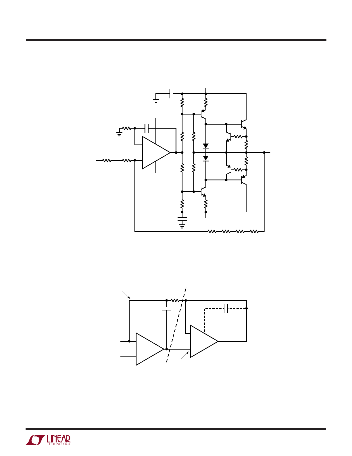
Application Note 86
R
SELECT
TYPICAL
INPUT FROM DAC
*
HEAT SINK
**
VISHAY VHP-100 RESISTOR 0.01%
***
1% METAL FILM RESISTOR
6Ω
Figure F3. High Voltage Output Stage Delivers ±100V at 25mA. Multiple
Feedback Resistors Minimize Dissipation and Voltage Coefficient Effects
***
10k
19.994k**
0.005µF
–
LTC1152
+
15V
–15V
1µF
1µF
1M50k
1M50k
125V
Q1
2N5415
Q2
2N3440
–125V
330Ω510Ω
2N2222
1N4148
1N4148
2N2907
330Ω510Ω
Q3
2N3440*
1k
Q5
27Ω
OUTPUT
27Ω
1k
Q6
Q3
2N5415*
100k**100k**100k**100k**
AN86 FF03
FROM TEXT FIGURE 2
(PARTIAL)
2k
0.1µF
0.1µF
(OPTIONAL—
FOR INCREASED
LOAD STABILITY)
C
C
AN86 FF04
FROM
MSB
AND LSB
DACs
–
LT1001
+
–
+
LT1206: 250mA OUTPUT
LT1210: 1.1A OUTPUT
Figure F4. LT1206/LT1210 Output Stages Supply 250mA and 1.1A Loads,
Respectively. Remote Sensing Is Usually Necessary to Compensate IR Drops
AN86-39
Page 40

Application Note 86
APPENDIX G
MEASURING DAC SETTLING TIME
Measuring the 20-bit DAC’s output settling time is a
challenging task. Although the time scale involved is
relatively slow, the 5µV LSB step size presents problems.
The issue reduces to obtaining a great deal of gain without
inducing overdrive in the monitoring oscilloscope. Such
overdrive will corrupt the measurement, rendering displayed results meaningless.
Figure G1 is a solution. The DAC output is resistively
balanced against a precision variable reference supply,
adjustable in 0.5µV steps.1 The circuit’s remainder constitutes a clamped, distributed gain of 2000 amplifier. Diode
clamping, placed at each gain stage input, prevents saturation from occurring even with large DAC-reference supply imbalances. The distributed gain allows 10kHz
bandwidth while maintaining clamping effectiveness. The
monitoring oscilloscope, operating at 5mV or 10mV/DIV
(5µV to 10µV at the DAC output), can readily discern 5µV
settling without incurring deleterious overdrive.
Layout and construction of this circuit requires care.
Figure G2 shows construction details. A linear layout
minimizes parasitic feedback paths, preventing oscillation. The DAC input step is fully shielded, preventing
feedthrough to various sensitive points within the amplifier. Finally, the entire circuit is built into a shielded
enclosure to minimize effects of stray RF and pick up.
The circuit is tested by applying a test step that settles
much faster than the DAC. Figure G3 uses a mercury
wetted reed relay based pulse generator to supply the step.
The unit noted is commercially produced, although similar
results are obtainable with standard mercury based reed
relays. When the relay opens the circuit’s output settles
essentially instantaneously (Figure G4) relative to DAC
speed and settling time amplifier bandwidth.
Figure G1’s response is tested by grounding one of its
inputs and driving the other with the pulse generator.
Figure G5 shows settling to within 1ppm (±5µV) in 2ms.
This is much faster than the DAC settles, lending confidence to text Figures 6 and 7 indicated results.
0V TO –5V
IN 0.5µV STEPS
FROM BUFFERED
KVD BIASED FROM
–5V REFERENCE
OUTPUT
0V TO 5V
*
VISHAY VHD-200 RATIO SET 10ppm MATCHING
1N4148
1N5712
CONNECT OUTPUT DIRECTLY TO
OSCILLOSCOPE. DO NOT USE CABLE
TO SET ZERO, GROUND BOTH INPUTS
AND ADJUST “ZERO” FOR V
FROM
DAC
20k*
20k*
OUT
= <1mV
5pF
+
LT1008
–
5pF
5pF
5.1k
9k
1k
+
LT1008
–
5.1k
9k
1k
+
LT1008
–
10k
ZERO
5.1k
9k
1k
10Ω909k
–15V15V
Figure G1. Clamped, Distributed Gain-of-2000 Amplifier Permits
DAC Settling Time Measurement Without Saturation Effects
Note 1: See Appendix C for details on such a supply.
+
LT1008
–
20pF
5.1k
5.1k
5.1k
OUTPUT
AN86 FG01
AN86-40
Page 41
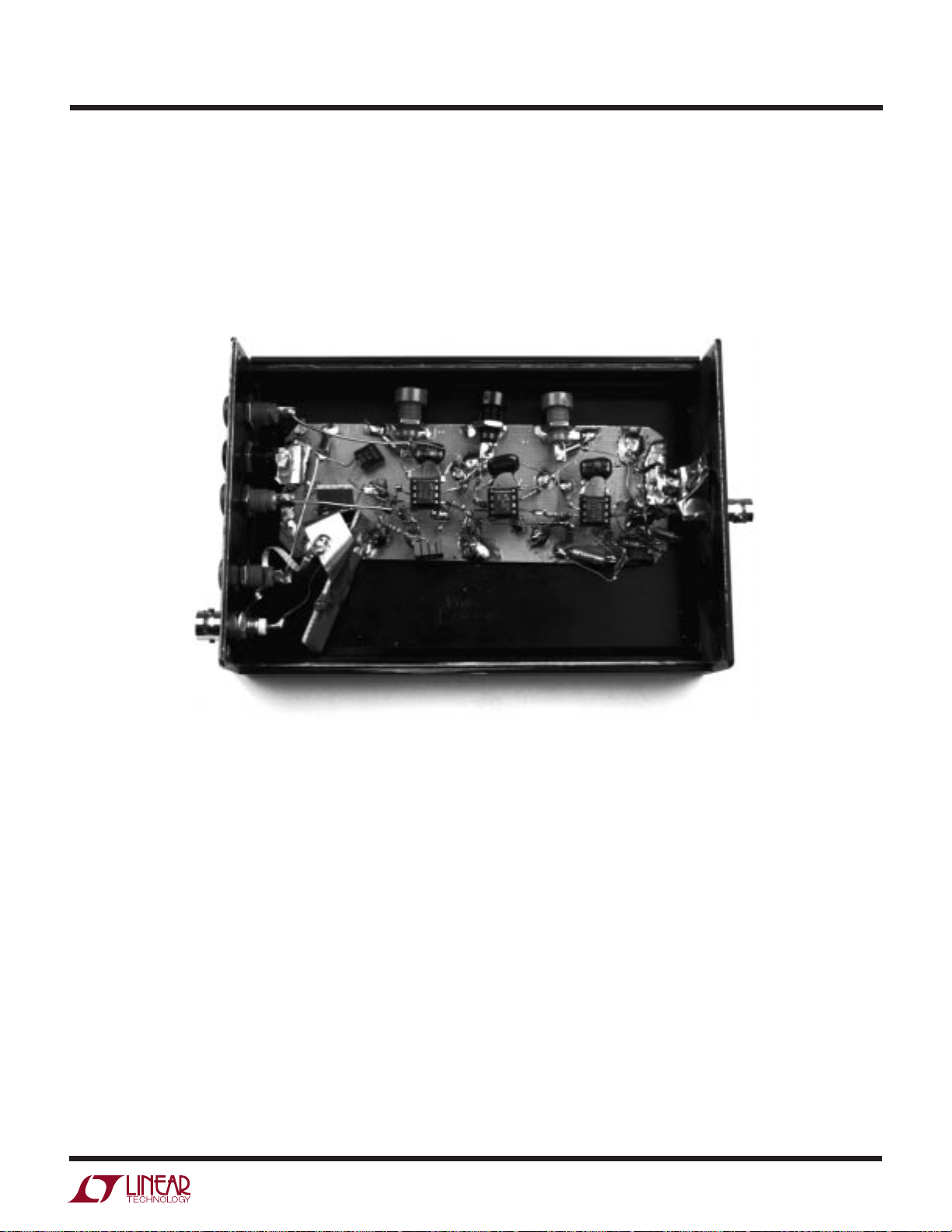
Application Note 86
AN86 FG02.tif
Figure G2. Settling Time Amplifier Construction. Bandwidth Is Only 10kHz, Although Gain of 2000 Necessitates Layout Care to Avoid
Parasitic Feedback Induced Oscillation. Input (Photo Lower Left) Is Fully Shielded, Preventing Radiative Feedthrough to Amplifier.
Enclosure Shields Circuit from Stray RF and Pickup
AN86-41
Page 42

Application Note 86
TEKTRONIX
067-0608-00
FROM
PULSE
GENERATOR
PULSE
IN
+V
Hg REED RELAY
50Ω
OUTPUT
TO DAC INPUT OF
SETTLE CIRCUIT
(GROUND SETTLE CIRCUIT
REFERENCE INPUT)
25ms
5V
30ms
AN86 FG03
Figure G3. Reed Relay Based Pulser Supplies Clean Step to Test Settling Time Circuit
AN86 FG03.tif
Figure G4. Mercury Wetted Reed Relay Opens in 5 Nanoseconds, Settles Quickly to Zero.
500MHz Ring-Off Derives from Source-Termination Impedance Mismatch
10µV/DIV
HORIZ = 2ms/DIV AN86 FE03.tif
Figure G5. Settling Time Circuit Responds to Test Step with 2ms Settling to ±1ppm (±5µV)
AN86-42
Page 43
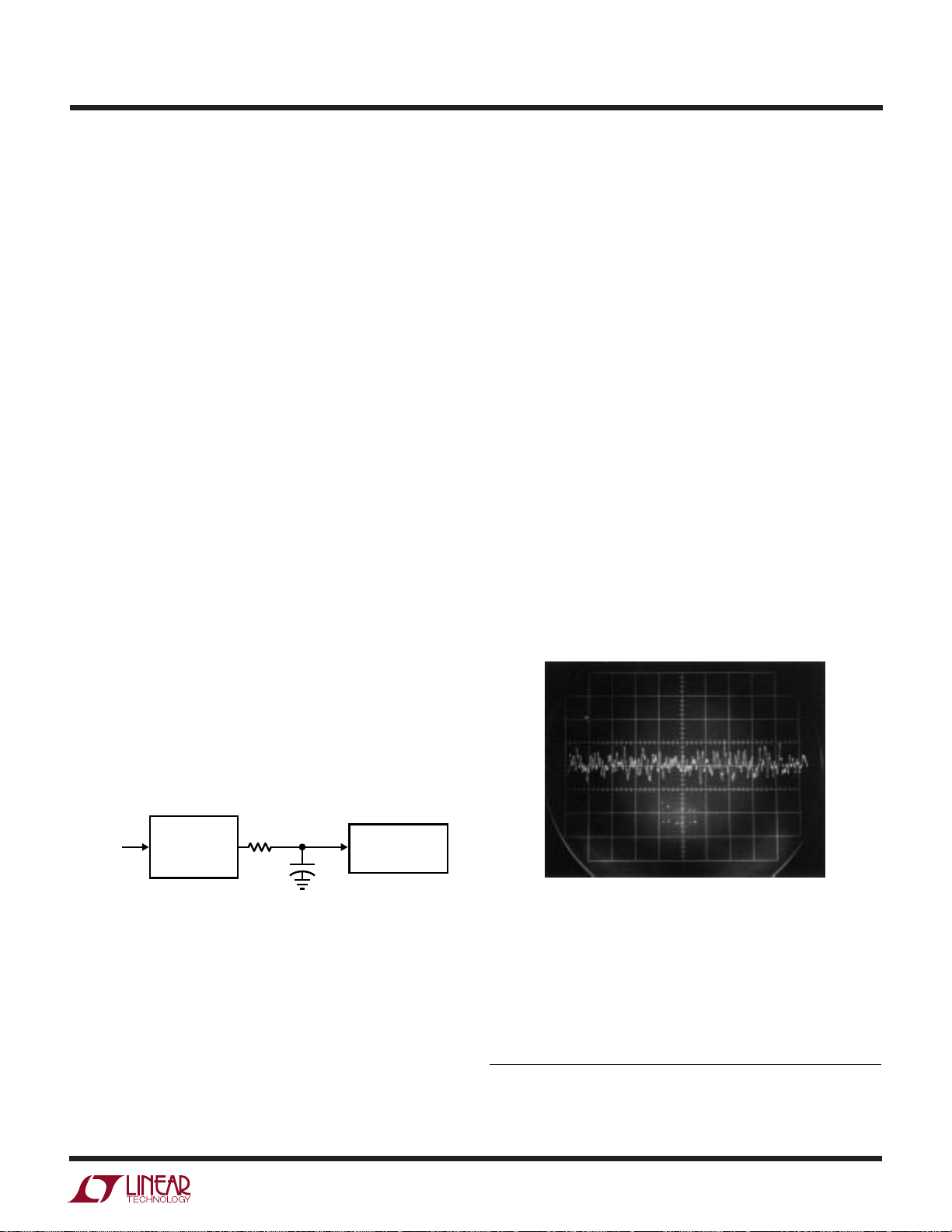
APPENDIX H
MICROVOLT LEVEL NOISE MEASUREMENT
Application Note 86
Verifying DAC output noise requires a quiet, high gain
amplifier at the oscilloscope. Figure H1 shows one way to
take the measurement. The input preamplifier, operating
at a gain of 1000, supplies a high pass cutoff at 0.1Hz. It
drives the oscilloscope via a 10Hz discrete low pass filter.
The oscilloscope, set to 1mV/DIV, indicates 1µV/DIV
referred to the preamplifier input. Figure H2 indicates DAC
output noise well below an LSB, about 0.9µV. Equipment
limitations set measurement noise floor at 0.2µV.
Figure H3 shows the noise measurement test setup. Note
that the signal levels involved dictate a completely shielded,
coaxial path from breadboard to oscilloscope.
Figure H4 lists some applicable high sensitivity amplifiers
suitable for the noise measurement. Current generation
oscilloscopes rarely have greater than 2mV/DIV sensitivity, although older instruments offer more capability. The
figure lists representative preamplifiers and oscilloscope
plug-ins suitable for noise measurement. These units
feature wideband, low noise performance. It is particularly
significant that many of these instruments are no longer
produced. This is in keeping with current instrumentation
trends, which emphasize digital signal acquisition as
opposed to analog measurement capability.
The monitoring oscilloscope should have exceptional trace
clarity. In the latter regard high quality analog oscilloscopes are unmatched. The exceptionally small spot size
of these instruments is well-suited to low level noise
measurement.1 The digitizing uncertainties and raster
scan limitations of DSOs impose display resolution penalties. Many DSO displays will not even register the fine
structure of the noise waveform.
FROM
DAC
OUTPUT
Figure H1. Microvolt Noise Measurement Necessitates High
Gain Preamplifier for Oscilloscope. Preamplifier and Discrete
Filter Set 0.1Hz to 10Hz Measurement Bandpass
PREAMPLIFIER
A = 1000
HIGH PASS
CUTOFF = 0.1Hz
1.6k
(10Hz)
+
10µF
OSCILLOSCOPE
1mv/DIV = 1µV/DIV
AN86 FH01
500nV/DIV
2s/DIV AN86 F04.tif
Figure H2. Indicated DAC Output Noise in a 0.1Hz to 10Hz
Bandpass Is Below 1µV, About 0.2LSB. Equipment
Limitations Set Measurement Noise Floor at 0.2µV
Note 1: In our work we have found Tektronix types 453, 453A, 454,
454A, 547 and 556 excellent choices. Their pristine trace presentation
is ideal for discerning small signals of interest against a noise floor
limited background.
AN86-43
Page 44

Application Note 86
Figure H3. Noise Measurement Test Setup Includes Shielded DAC Breadboard (Foreground), Preamplifier
(Left) and Low Pass Filter Attached to Oscilloscope (Center). Measurement Path Is Fully Coaxial
AN86-44
AN86 FH03.tif
Page 45

Application Note 86
INSTRUMENT MODEL MAXIMUM
TYPE MANUFACTURER NUMBER BANDWIDTH SENSITIVITY/GAIN AVAILABILITY COMMENTS
Differential Amplifier Tektronix 1A7/1A7A 500kHz/1MHz 10µV/DIV Secondary Market Requires 500 Series Mainframe,
Settable Bandstops
Differential Amplifier Tektronix 7A22 1MHz 10µV/DIV Secondary Market Requires 7000 Series Mainframe,
Settable Bandstops
Differential Amplifier Tektronix 5A22 1MHz 10µV/DIV Secondary Market Requires 5000 Series Mainframe,
Settable Bandstops
Differential Amplifier Tektronix ADA-400A 1MHz 10µV/DIV Current Production Standalone with Optional Power
Supply, Settable Bandstops
Differential Amplifier Tektronix AM-502 1MHz 100,000 Secondary Market Standalone with Optional Power
Supply, Settable Bandstops
Differential Amplifier Preamble 1822 10MHz Gain = 1000 Current Production Standalone, Settable Bandstops
Differential Amplifier Stanford Research SR-560 1MHz Gain = 50000 Current Production Standalone, Settable Bandstops,
Systems Battery or Line Operation
Figure H4. Some Applicable High Sensitivity, Low Noise Amplifiers.
Trade-Offs Include Compatibility, Sensitivity and Availability
APPENDIX I
VOLTAGE REFERENCES
Figure I1 lists some voltage reference options for use with
the DAC. The self-contained types are convenient and
easily applied. The LM199A and the LTZ1000A require
external circuitry but offer higher performance. All choices
must be trimmed to establish absolute DAC accuracy. The
LTZ1000A offers the highest stability and is discussed
below.
Figure I2 shows the LTZ1000A and its support circuitry.
A1 senses LTZ1000A die temperature and accordingly
controls the IC heater via the 2N3904. A2 controls reference current. The Zener reference is sensed via Kelvin
connections, minimizing voltage drop effects. A single
point ground eliminates return current mixing and the
attendant errors that would be produced.
INITIAL TEMPERATURE LONG-TERM
TYPE VOLTAGE ACCURACY DRIFT STABILITY COMMENTS
LTZ1000A 7.2V Minimum 7V 0.05ppm/°C 4ppm/Yr Typical Highest Stability Zener Available. Requires
Maximum 7.5V External Heater Control and Reference Buffer Circuitry
LM199A 6.95V 2% 0.5ppm/°C 10ppm/Yr Typical Self-Contained, Including Heater Control Circuitry.
LT1021 5V, 7V, 10V 0.05V (7V) 2ppm/°C (7V) 20ppm/kHr Noncumulative Fully Self-Contained. Trimmable
LT1027 5V 0.02% 2ppm/°C 20ppm/kHr Noncumulative Fully Self-Contained. Trimmable
LT1236 5V, 10V 0.05% 5ppm/°C 20ppm/kHr Noncumulative Fully Self-Contained. Trimmable
Figure I3 offers choices for reference buffering. All employ
a chopper stabilized amplifier augmented with a buffer
output stage. Buffer error is extremely low, as noted in
Appendix C’s discussion. I3a, a simple unity-gain stage,
transmits the input to the output with low error and
minimal reference loading. I3b takes moderate gain, allowing a 7V reference input to produce (in this case) 10V
at the output. I3c offers two ways to get 5V from the
nominal 7V input. A precision divider lightly loads
the reference in one case; the 5V output is taken at the
LT1010. Reference loading is avoided by placing the
divider at the output (optional case shown) and driving the
A-to-D reference input from the divider output, which is
permissible.
Zener Output Is Unbuffered
Figure I1. Reference Choices Compared for Output Voltage, Accuracy
and Stability. Highest Stability Types Require External Circuitry
AN86-45
Page 46

Application Note 86
2N3904
R1 THROUGH R5:
VISHAY VHP-100 0.1%
1k
A1
LT1013
ZENER + SENSE
+
V
15V
3
R4
13k
R3
70k
+
–
10k
1M
0.1µF
8
6
TEMP
SENSOR
7
4
5
7
R2
70k
1N4148
+
A2
LT1013
–
ZENER – SENSE
HEATER,
UNLABELED
AND
ZENER = LTZ1000A
PIN NUMBERS APPEAR
FOR INDIVIDUAL
LTZ1000A ELEMENTS
1
HEATER
2
0.1µF
R5
1k
1N4148
R1
120Ω
0.022µF
ZENER – FORCE
HEATER RETURN
Figure I2. 7V Reference Includes A1 Heater Control Amplifier, A2 Zener Current Regulator
and LTZ1000A Zener. Note Zener Kelvin Connections and Single Point Ground
10k
0.1µF
–
TO ZENER
SENSE
TO ZENER
SENSE
12.9k**
LTC1150
+
–
LTC1150
+
LT1010
5k**
0.1µF
LT1010
OUT = 7.2V NOMINAL
OUT = 10V NOMINAL
SINGLE
POINT
GROUND
AN86 FI02
AN86-46
–
TO ZENER
SENSE
VISHAY VHP-100 – 1%
*
VISHAY VHD-200 RATIO SET – 0.1%
**
22k*
+
50k*
Figure I3. Chopper Stabilized Reference Buffer Options Include Unity Gain (a),
10V (b) and 5V (c) Output. Trimming Is Required for Absolute Accuracy
LTC1150
0.1µF
10k
LT1010
OUT = 5V NOMINAL
2.2k**
OUT = 5V NOMINAL
5k**
OPTIONAL, DELETE INPUT DIVIDER.
SEE TEXT
AN86 I03
Page 47

Application Note 86
DEGREES CENTIGRADE
25 30 35 40 45
MICROVOLTS REFERRED TO 25°C
AN86 FJ02
3.0
2.8
2.6
2.4
2.2
2.0
1.8
1.6
1.4
1.2
1.0
0.8
0.6
0.4
0.2
0
APPENDIX J
CABLES, CONNECTIONS, SOLDER, COMPONENT
CHOICE, TERROR AND ARCANA
Subtle parasitic effects can have pronounced and seemingly inexplicable effects on low level circuit performance.
Perhaps the most prevalent detractor to microvolt level
circuitry is unintended thermocouples. Considerable discussion for dealing with thermocouples appeared in Appendix C and should be considered preliminary to this
section’s material.
In 1822, Thomas Seebeck, an Estonian physician, accidentally joined semicircular pieces of bismuth and copper
(Figure J1) while studying thermal effects on galvanic
arrangements. A nearby compass indicated a magnetic
disturbance. Seebeck experimented repeatedly with different metal combinations at various temperatures, noting
relative magnetic field strengths. Curiously, he did not
believe that electric current was flowing and preferred to
describe the effect as “thermomagnetism.” He published
his results in a paper, “Magnetische Polarisation der
Metalle und Erze durch Temperatur-Differenz” (see References).
JUNCTION
In low drift circuits, unwanted thermocouples are probably the primary source of error. Connectors, switches,
relay contacts, sockets, wire and even solder are all
candidates for thermal EMF generation. It is relatively clear
that connectors and sockets can form thermal junctions.
However, it is not at all obvious that junctions of wire from
different manufacturers can easily generate 200nV/°C—
four times a precision amplifier’s drift specification! Figure J2 shows a plot obtained for such a wire junction. Even
solder can become an error term at low levels, creating a
junction with copper or Kovar wires or PC traces (see
Figure J3). Figure J4 lists thermocouple potentials for
some common materials found in electronic assemblies.
N
WE
S
COMPASS
Figure J1. The Arrangement for Dr. Seebeck’s
Accidental Discovery of “Thermomagnetism”
Subsequent investigation has shown the “Seebeck Effect”
to be fundamentally electrical in nature, repeatable and
quite useful. Thermocouples, by far the most common
transducer, are Seebeck’s descendants. Unfortunately,
unintended and unwanted thermocouples are also
Seebeck’s progeny.
COPPER
JUNCTION
BISMUTH
AN86 FJ01
Figure J2. Thermal EMF Generated by Two “Identical”
Copper Wires Due to Oxidation and Impurities
100
50
0
IN MICROVOLTS
–50
THERMALLY PRODUCED VOLTAGE
–100
SOLDER-COPPER JUNCTION DIFFERENTIAL TERMPERATURE
SLOPE ≈ 1.5µV/°C BELOW 25°C
64% Sn/36% Pb
60% Cd/40% Sn
SLOPE ≈ 160nV/°C BELOW 25°C
10 20 30 40 50
0
SOURCE: NEW ELECTRONICS 2/6/77
AN86 FJ03
Figure J3. Solder-Copper Thermal EMFs. Cd/Sn Has Notably
Lower Activity but Is Toxic, Not Available and Not Recommended
AN86-47
Page 48

Application Note 86
The unusually energetic response of Cu-CuO necessitated
the treatment described in Appendix C (Figure C7 and
associated text) for cleaning DVM and Kelvin-Varley divider connections. Readers finding this figure’s information seemingly academic should be awakened by Figure
J5. This chart lists thermoelectric potentials for commonly employed laboratory connectors. Thermocouple
activity of some types is more than 20 times greater than
others. Be careful!
Minimizing thermal EMF induced errors is possible if
judicious attention is given to circuit board layout. In
general, it is good practice to limit the number of junctions
in the signal path. Avoid connectors, sockets, switches
and other potential error sources to the extent possible. In
some cases this will not be possible. In these instances,
attempt to balance the number and type of junctions in the
signal path so that differential cancellation occurs. Doing
this may involve deliberately creating and introducing
junctions to offset unavoidable junctions. This can be a
tricky procedure. Repeated deliberate temperature excursions may be necessary to determine the optimal number
and placement of added junctions. Experimentation, tempered by a healthy reserve of patience and abundance of
time, is required. This practice, borrowed from standards
lab procedures, can be quite effective in reducing thermal
EMF originated drifts. Figure J6 shows a simple example
where a nominally unnecessary resistor is included to
promote such thermal balancing. For remote signal sources
connectors may be unavoidable. In these cases, choose a
connector specified for relatively low thermal EMF activity
and ensure a similarly balanced approach in routing signals through the connector along the circuit board and to
circuitry. If some imbalance is unavoidable, deliberately
introduce an intentional counterbalancing junction. In all
cases maintain the differencing junctions in close physical
proximity, which will keep them at the same temperature.
Avoid drafts and temperature gradients, which can introduce thermal imbalances and cause problems. Figure J7
shows the LTC1150 set up in a test circuit to measure its
temperature stability. The lead lengths of the resistors
connected to the amplifier’s inputs are identical. The
thermal capacity each input sees is also balanced because
of the symmetrical connection of the resistors and their
identical size. Thus, thermal EMF induced shifts are equal
in phase and amplitude and cancellation occurs. Very
slight air currents can still affect even this arrangement.
Figure J8 shows a strip chart of output noise with the
circuit covered by a small styrofoam cup (HANDI-KUP
TM
Company Model H8-S) and with no cover in “still” air. This
data illustrates why it is often prudent to enclose low level
circuitry inside some form of thermal baffle.
AN86-48
MATERIALS POTENTIAL (µV/°C)
Cu-Cu < 0.2
Cu-Ag 0.3
Cu-Au 0.3
Cu-Cd/Sn 0.3
Cu-Pb/Sn 1 to 3
Cu-Kovar 40
Cu-Si 400
Cu-CuO 1000
Source: Low Level Measurements,
Keithley Instruments, 1984
(see References)
Figure J4. Thermoelectric Potentials for Various Materials
Indicates Inadvisability of Mixing Materials in Signal Path.
Cu-Cu Connections (Chart Top) Must Be Kept Clean or
5000:1 Degradation Occurs As They Oxidize (Chart Bottom)
HANDI-KUP is a trademark of WinCup.
Page 49

Application Note 86
THERMOELECTRIC
CONNECTION TYPE DESCRIPTION POTENTIAL (µV/°C)
BNC-BNC Mate 0.4
BNC-Banana Adapter 0.35
BNC-BNC “Barrel” Adapter 0.4
Male/Female Banana Mate Sample #1 0.35
Male/Female Banana Mate Sample #2 1.1
Male/Female Banana Mate (Type Specified 0.07
for Low Thermal Activity) Sample #3
Copper Lug-Copper Banana Binding Post 0.08
Copper Lug-Standard Banana Binding Post 0.5
Plated Lug-Copper Banana Binding Post 1.7
Figure J5. Measured Thermoelectric Potentials for Some Common Laboratory Connectors.
Pronounced Difference Between “Banana” Samples Is Due to Manufacturer’s Materials Choice. Note
That Copper Lug/Copper Banana Post Has 20× Lower Activity Than Plated Lug/Copper Banana Post
AN86-49
Page 50
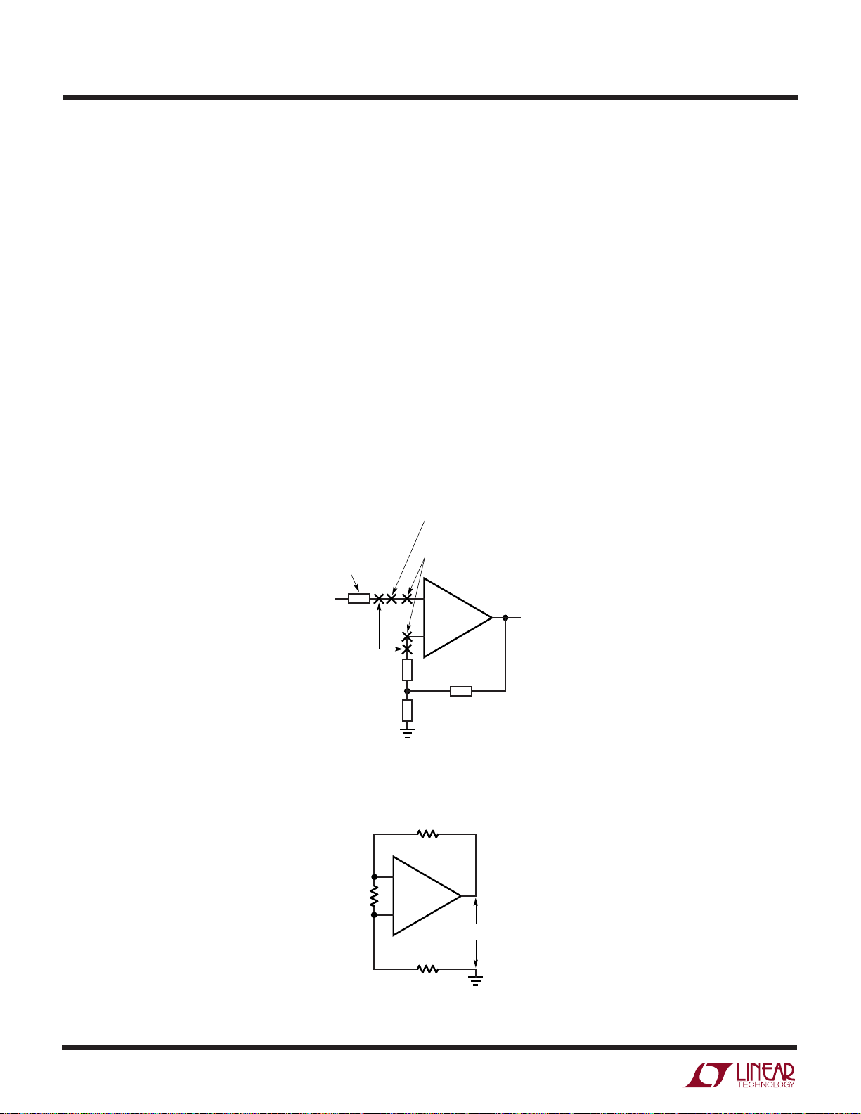
Application Note 86
Thermal EMFs are the most likely, but not the only,
potential low level error source. Electrostatic and electromagnetic shielding may be required. Power supply transformer fields are notorious sources of errors often
mistakenly attributed to amplifier DC drift and noise. A
transformer’s magnetic field impinging on a PC trace can
easily generate microvolts across that conductor in accordance with well known magnetic theory. The circuit cannot
distinguish between this spurious signal and the desired
input. Attempts to eliminate the problem by rolling off
circuit response may work, but often the filtered version of
the undesired pickup masquerades as an unstable DC
term. The most direct approach is to use shielded transformers but careful layout may be equally effective and
less costly. A circuit that requires the transformer to be
close by to achieve a good quality grounding scheme may
be disturbed by the transformer’s magnetic field. An RF
NOMINALLY UNNECESSARY
RESISTOR USED TO
THERMALLY BALANCE OTHER
INPUT RESISTOR
choke connected across a scope probe can determine the
presence and relative intensity of transformer fields, aiding layout experimentation.
Another source of parasitic error is stray leakage current.
Such leakage currents must be prevented from influencing circuit operation. The simplest way to do this is to
connect leakage sensitive points via teflon standoffs.
Because the points never contact the PC board, stray
leakage currents do not affect them. Although this approach is effective, its implementation may not be acceptable in production. Guarding is another technique for
minimizing board leakage effects. The guard is a PC trace
completely encircling the leakage sensitive points. This
trace is driven at a potential equal to that of the point,
preventing leakage to the “guarded” point. On PC boards,
the guard should enclose the node(s) to be protected.
Guarding was used to eliminate the effects of capacitor
surface leakage in Appendix C’s Figure C7.
DELIBERATE SPLICE MAY BE DESIRABLE
TO BALANCE OTHER JUNCTIONS
LEAD WIRE/SOLDER/COPPER
TRACE JUNCTION
+
OUTPUT
RESISTOR LEAD, SOLDER,
COPPER TRACE JUNCTION
Figure J6. Typical Thermal Layout Considerations Emphasize Minimizing and Differencing
Parasitic Thermocouples. Thermal Mass at Amplifier Inputs Should Be Equal, Allowing
Differenced Parasitic Thermocouple Outputs to Arrive Matched In Phase and Amplitude
100Ω
Figure J7. Amplifier Drift Test Circuit. Thermal EMFs and Thermal
Capacity at Each Input Must Be Similar for Cancellation to Occur
–
AN86 FJ06
50k
–
LTC1150
+
EOS × 1000
50k
AN86 FJ06
AN86-50
Page 51

Application Note 86
AN86 FJ08.tif
Figure J8. Effect of Thermal Baffle on Low Frequency Amplifier Noise in “Still” Air. Amplifier Is Covered
By Small Cup in Upper Trace, Uncovered in Lower Trace. Instability Worsens If Air Movement Increases
AN86-51
Page 52

Application Note 86
AN86-52
Linear Technology Corporation
1630 McCarthy Blvd., Milpitas, CA 95035-7417
(408) 432-1900 ● FAX: (408) 434-0507
●
www.linear-tech.com
an86f LT/TP 0101 4K • PRINTED IN USA
LINEAR TECHNOLOGY CORPORATION 2001
 Loading...