

Page 1
Application Note 76
May 1999
OPTI-LOOP Architecture Reduces Output Capacitance and
Improves Transient Response
John Seago
INTRODUCTION
Removing output capacitors saves money and board
space. Linear Technology’s OPTI-LOOPTM architecture
allows you to use the output capacitors of your choice and
compensate the control loop for optimum transient
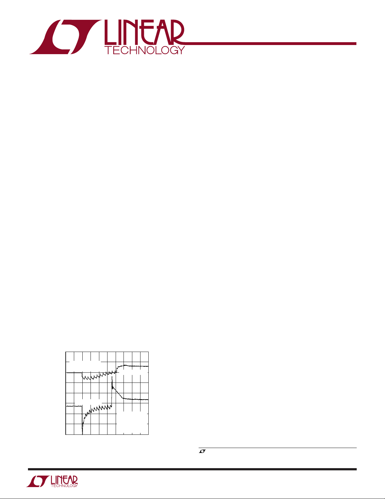
response and loop stability. Figure 1 shows the dramatic
improvement possible with the OPTI-LOOP architecture.
With the improvement shown in Figure 1, less capacitance
is required or less expensive capacitors can be used. Load
dynamics and supply tolerances will predict the minimum
output capacitance required. The quality of loop compensation determines how close you can get to this minimum
capacitance requirement in a real world system.
One of the least understood areas of power supply design
is control loop compensation. Because of this, some
manufacturers provide loop compensation inside the regulator IC. Internal compensation works best with one set of
operating conditions and is sensitive to output capacitor
characteristics. Consequently, more expensive output
capacitors may be required to stabilize the loop because of
the sensitivities of the internal IC compensation. The
OPTI-LOOP architecture is intended to allow circuit
designers to squeeze the most performance out of the
output capacitors of their choice.
OPTI -LOOP
COMPENSATION
C
OUT
= 1500µF
WHAT IS LOOP COMPENSATION?
Loop compensation is the adjustment of the control loop
frequency response to assure loop stability and optimize
the transient response of the power supply. The frequency
response is determined by the gain and phase of the loop’s
reaction to load current changes at all frequencies. A Bode
plot is used to show the gain and phase of the frequency
response.
LOOP COMPENSATION BASICS
This application note contains a brief refresher course in
control loop basics. Frequency response is characterized
by the effects of poles and zeros. Each pole has a corner
frequency, caused by a resistance and capacitance, that
determines the beginning of a 20dB/decade drop in voltage gain. The pole also causes the phase to decrease by
90°, starting roughly one decade before the corner frequency and ending about one decade after the corner
frequency. A zero has the opposite effect of a pole. It
causes the gain to increase by 20dB/decade starting at its
“RC” corner frequency and it adds 90° of phase shift,
starting one decade before the corner frequency and
ending one
decade after the corner frequency. The effects of poles and
zeros are additive, so that two poles at the same frequency
cause a 40dB/decade roll-off in gain and a 180° phase shift
over two decades. If a pole and zero occur at the same
frequency, their effects cancel.
COMPETITION
OUTPUT VOLTAGE (50mV/DIV)
TIME (10µs/DIV)
Figure 1. Improved Transient Response with
OPTI-LOOP Architecture
VIN = 15V
= 1.6V
V
O
I
= 30mA to 7A
O
= 1500µF
C
OUT
DSOL8 F01
The crossover frequency of the loop determines the bandwidth and transient response of the power supply. The
crossover frequency is the frequency at which the loop
gain is one (0dB). The higher the crossover frequency, the
faster the power supply can respond to changes in load
current.
, LTC and LT are registered trademarks of Linear Technology Corporation.
OPTI-LOOP is a trademark of Linear Technology Corporation.
AN76-1
Page 2
Application Note 76
In a voltage mode DC/DC switching regulator system, the
buck inductor and output capacitor form a double pole at
their resonant frequency, causing a 40dB/decade gain
roll-off and 180° phase shift. Since the inductor’s effect on
a current mode control loop is largely cancelled by the
current loop, it is generally easier to compensate a current
mode regulator than a voltage mode regulator.
The first requirement of loop compensation is stability. If
the error amplifier’s feedback becomes positive when the
loop gain equals one, the regulator will oscillate. A loop
oscillation appears as a sine wave riding on the DC output
voltage at the unity-gain frequency of the control loop.
This oscillation will generally occur in the frequency range
of 1kHz to 20kHz. Don’t confuse switching frequency
ripple or higher frequency ringing with a loop instability.
If a network analyzer is available, stability margins can be
determined by measuring the gain and phase of the loop
and observing the resulting Bode plot. The phase margin
is the difference between the signal phase and –360°
when the voltage gain is one (0dB). A 60° phase margin is
preferred, but 45° is usually acceptable. The gain margin
is the amount of negative gain present when the signal
phase is zero (– 360°). A gain margin of – 10dB is normally
considered acceptable. Generous gain and phase margins
are very important because actual component values vary
over temperature and component values differ from unit to
unit in production, causing the loop’s voltage gain and
phase to vary accordingly. If the component values cause
the phase to go to zero when the voltage gain is one, the
regulator will oscillate. The goal is to provide the best gain
and phase margins with the highest crossover frequency
possible. A high crossover frequency results in a quick
response to load current changes whereas high gain at low
frequencies results in fast settling of the output voltage.
Nonideal components and amplifier gain limitations generally force a trade-off between high crossover frequency
and large stability margins.
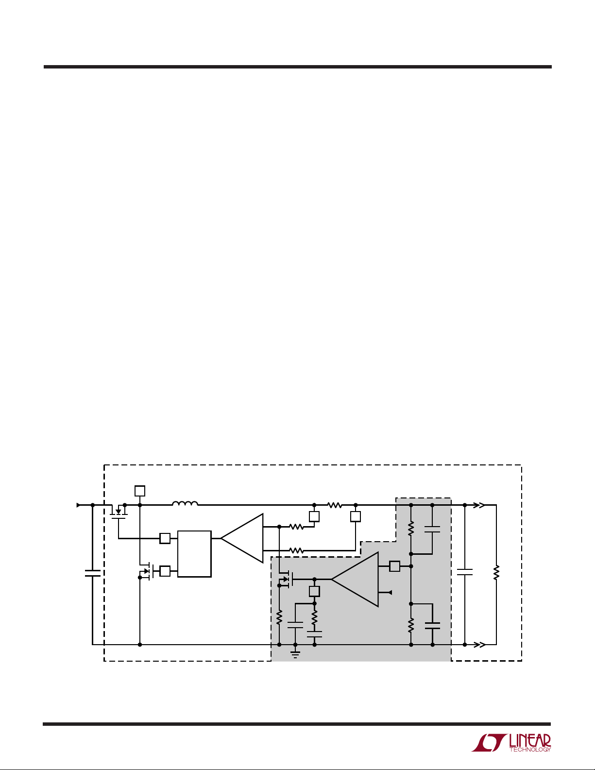
THE CONTROL LOOP
Figure 2 shows the simplified control loop for the LTC®1628
and LTC1735/LTC1736 current mode, synchronous buck
regulators. The control loop has both DC gain and AC
frequency response characteristics. The DC loop consists
of the feedback resistors, the error amplifier, the DC
resistance of the ITH pin components, the current comparator, the sense resistor and the load resistor. The AC
loop consists of the DC loop plus the output capacitor,
capacitors C1 and C2 and the AC impedance of the ITH pin
components.
INPUT
C
IN
AN76-2
TOP
MOSFET
BOTTOM
MOSFET
SWITCH
NODE
(LTC1735/LTC1736)
INDUCTOR
TG
BG
LTC1628
MOSFET
CONTROL
LOGIC
+
CURRENT
COMP
–
MODULATOR ERROR AMPLIFIER
30k
30k
R
SENSE
SENSE
(10mV TO 65mV)
0V TO 75mV
(0.3V TO 2.2V)
0.3V TO 2.4V
I
TH
C4
R3
C3
+
ERROR
AMP
gm = 1.4mS
SENSE
+
–
–
V
OSENSE
0.8V
Figure 2. Basic Control Loop of Current Mode, Switching Regulator
OUTPUT
R1
C1
C
R
OUT
LOAD
C2
R2
AN76 F02
Page 3

Application Note 76
DC GAIN
DC gain is the small-signal loop gain under static test
conditions. Load regulation is determined by DC gain, so
the higher the gain, the lower the change in output voltage
for a given DC load current variation. The DC gain is the
product of the feedback resistor attenuation, the error
amplifier voltage gain and modulator gain. The modulator
consists of the current comparator, the MOSFETs and
their drivers, the inductor, sense resistor, output capacitor
and load resistance: basically the power path.
The feedback divider attenuation is:
A
= V
V(FB)
where: V
V
is the output voltage of the power supply.
OUT
REF/VOUT
is 0.8V for products in the LTC1735 family and
REF
The error amplifier voltage gain is:
A
= g
V(EA)
where: g
m(EA)ZITH
is the transconductance of the error ampli-
m(EA)
fier, 1.4mS for products in the the LTC1735 family and
Z
is the output impedance of the error amplifier in
ITH
parallel with any impedance connected to the ITH pin.
g
m(MOD)
= (V
RSENSE(MAX)/RSENSE
)/∆V
ITH(MAX)
= (0. 075V/0.015Ω)/2.1V = 2.38S
A
V(MOD)
= g
m(MOD)RLOAD
= (2.38S)(3.3V/3A)
= 2.62 = 8.4dB
DC Gain = (A
V(FB)
)( A
V(EA)
)(A
V(MOD)
)
= (0.242)(4592)(2.62) = 2911 = 69.3dB
FREQUENCY RESPONSE
Frequency response is the loop’s reaction to perturbations
at all frequencies and is shown as gain and phase measurements on a Bode plot. The output capacitor and load
resistance largely determine where the error amplifier
poles and zeros need to be placed for optimum transient
response and loop stability.
Output Capacitor Pole and Zero
The gain at very low frequencies is equal to the DC gain.
Normally the first departure from that gain is the pole
created by the load resistance and the output capacitance.
The corner frequency of this pole is:
The transconductance of the modulator must be determined before calculating the modulator gain. The modulator transconductance is:
g
m(MOD)
where: V
R
SENSE
∆V
ITH(MAX)
= (V
RSENSE(MAX)/RSENSE
RSENSE(MAX)
is listed in the data sheet as 75mV,
)/∆V
ITH(MAX)
is the value of the current sense resistor and
is 2.1V for the no-load to full-load output
voltage swing of the error amplifier.
The DC voltage gain of the modulator is:
A
where: g
and R
V(MOD)
m(MOD)
LOAD
= g
m(MOD)RLOAD
is the transconductance of the modulator
= V
OUT/IOUT
.
As an example, the DC gain for the LTC1735/LTC1736 or
the LTC1628 providing 3A at 3.3V is:
A
V(FB)
A
V(EA)
= V
= g
/V
REF
OUT
m(EA)ZITH
= 0.8V/3.3V = 0.242 = –12.3 dB
= (1.4mS)(3.28M) = 4592 = 73.2 dB
where: 3.28M is the typical output impedance of the error
amplifier without any external DC loading on the ITH pin.
fP = 1/(2πRLC
where: RL is the load resistance and C
OUT
)
is the output
OUT
capacitance.
Notice that as the output current goes down, the equiva-
lent load resistance goes up, causing the pole frequency to
decrease. The same is true when the output capacitance
increases, that is, the pole frequency moves lower.
The amount of phase margin is largely determined by the
zero formed by the output capacitance and capacitor ESR.
The corner frequency of this zero is:
fZ = 1/(2πESR • C
OUT
)
It is interesting to note that doubling the number of like
output capacitors will lower the pole frequency by half but
will not change the zero frequency of the output capacitor.
This is true because, as the capacitance doubles, the ESR
is halved, yet the load resistance remains the same.
Consequently, the product of RL and C
product of ESR and C
remains the same. It is desirable
OUT
goes up, but the
OUT
that the crossover frequency be higher than the ESR zero
AN76-3
Page 4
Application Note 76
frequency because the phase shift of the ESR zero is very
helpful in achieving adequate phase margin.
Different types of capacitors have different amounts of
ESR per µF of capacitance. The ESR of the output capacitor
determines the output ripple voltage under static load
conditions and greatly affects the output response to
transient loads. For a 3A output, the inductor ripple current
should be about 1A
ESR should be about 0.05Ω for a 50mV
. Therefore, the output capacitor
P-P
output voltage
P-P
ripple. The difference in frequency response between
Panasonic’s Specialty Polymer output capacitors and aluminum electrolytic output capacitors, with 0.05Ω of ESR,
is shown in Figures 3 and 4.
40
47µF
6.3V
30
0.05Ω
20
= 1.1Ω
R
L
10
0
GAIN (dB)
–10
–20
–30
–40
GAIN
PHASE
110
Figure 3. Frequency Response of Specialty Polymer
Capacitor Used in 3.3V, 3A Power Supply Output
40
1200µF
6.3V
30
0.048Ω
20
RL = 1.1Ω
10
GAIN (dB)
–10
–20
–30
–40
12Hz
0
GAIN
PHASE
110
1
fZ =
2πESR(C
308Hz
100 10k1k
FREQUENCY (Hz)
1
fZ =
2πESR(C
fP =
120Hz
276Hz
100 10k1k
FREQUENCY (Hz)
fP =
)
OUT
fP =
3.08kHz
6.77kHz
fP =
)
OUT
27.6kHz
1.2kHz
fZ = 2.76kHz
1
2πR
LCOUT
677.6kHz
30.8kHz
fZ = 67.76kHz
100k
1
2πR
LCOUT
100k
1M
AN76 F03
1M
AN76 F04
PHASE (DEG)
45
0
–45
–90
–135
PHASE (DEG)
45
0
–45
–90
–135
Aluminum electrolytic capacitors are often selected for
both the input and output of very low cost power supplies.
Figure 3 shows a 3kHz pole for a 47µF, 6.3V, 0.05Ω
Specialty Polymer capacitor. Figure 4 shows a 120Hz pole
for a 1200µF, 6.3V, 0.05Ω aluminum electrolytic capaci-
tor. In order to maintain the 0.05Ω ESR required to meet
the output ripple requirement, the aluminum electrolytic
capacitor requires 25 times the capacitance of the Specialty Polymer capacitor, causing the aluminum electrolytic capacitor to have a pole frequency at 4% of the
specialty polymer capacitor.
The loop compensation must be quite different when
aluminum electrolytic capacitors are used. It is unlikely
that fixed internal compensation will work well with both
types of capacitors. Although bandwidth will suffer when
aluminum electrolytic capacitors are used, using an OPTILOOP architecture, the loop can be optimized for their use
and stable operation achieved. The high ESR zero frequency of the Specialty Polymer capacitors makes the
loop more difficult to compensate, but the bandwidth will
be significantly higher as a result of the extra effort.
The Modulator
The modulator controls the inductor current as a function
of the amplified error signal from the error amplifier. The
transconductance of the modulator, calculated earlier, is
determined by the maximum current allowed through the
sense resistor divided by the maximum voltage swing of
the error amplifier output at the ITH pin. The product of the
modulator transconductance and the load resistance is
the modulator gain for DC. The frequency response of the
modulator is determined by multiplying the modulator
gain at DC times the frequency response of the output
capacitor and the load resistance. This is the same as
changing the 0dB gain reference on Figures 3 and 4 to the
modulator gain level. Consequently, the frequency
response of the modulator is primarily determined by the
output capacitor and the load resistance.
Figure 4. Frequency Response of Aluminum Electrolytic
Capacitor Used in 3.3V, 3A Power Supply Output
AN76-4
Page 5

Application Note 76
The Error Amplifier
The error amplifier provides most of the loop gain. After
selecting the output capacitor, the control loop is compensated by tailoring the frequency response of the error
amplifier. It has a transconductance of 1.4mS and an
output resistance of 3MΩ, so it provides a low frequency
gain of 4600 or 73dB. The loop gain is the product of the
error amplifier gain and the modulator gain, so the frequency response of the error amplifier, the output capacitor and load resistor determine the frequency
response of the loop.
The AC behavior of the error amplifier is determined by C1,
C2, C3, C4, R1, R2 and R3 as shown in Figure 2. The
following relationships are given as a first approximation,
since there is some interaction between the parts. As an
example, the low frequency pole of the error amplifier is
the dominant pole and is determined primarily by C3 and
the output resistance of the error amplifier as shown by:
fP = 1/(2πR
However, R3 and C4 have a small effect on the actual
corner frequency, since the series combination of C3 and
R3 are in parallel with C4, which is in parallel with R
Although all three impedances interact, the resistance of
R3 is small compared to the impedance of C3 at the pole
frequency, so its effect is small. The same is true of C4.
Since the value of C4 is normally small compared to C3,
the primary effect is determined by C3.
Resistor R3 adds a zero to the frequency response to
control gain in the midfrequency range. This zero frequency is:
fZ = 1/(2πR3C3)
Capacitor C4 adds a pole to reduce very high frequency
gain. Although frequently unnecessary for loop stability,
C4 helps to filter the effects of PCB noise and output ripple
voltage from the loop. It is desirable to have the error
amplifier gain be less than zero dB at the switching
frequency. The high frequency pole created by C4 is:
fP = 1/(2πR3C4)
The high frequency zero created by C1 and R1 can be very
important for transient load applications. Capacitor C1
provides phase lead and acts like a speed-up capacitor to
output voltage changes, so it tends to “short-out” R1 and
O(EA)
C3)
O(EA)
.
improve the high frequency response. This zero tends to
produce a positive-going bump in the phase plot. Ideally,
the peak of this bump is centered over the loop’s crossover
frequency. The R1, C1 zero is located at:
fZ = 1/(2πR1C1)
The pole created by R2 and C2 is generally not critical for
loop stability. It is frequently set at one half to one third of
the switching frequency and is primarily used for noise
filtering rather than loop compensation. The effect of C2 is
normally countered by the value of R3. The R2, C2 pole
frequency can be calculated by:
fP = 1/(2πR2C2)
ITH PIN COMPONENT VALUES
Selecting the best values for the loop compensation components is not as simple as selecting pole and zero
frequencies for the ideal crossover frequency. Several
other factors should be taken into account. The slew rate
and amplitude of the load transient largely determine the
ESR requirement of the output capacitor. The amount of
capacitance used at the output is primarily determined by
the type of capacitor used and partially determined by the
load transient characteristics.
PCB-generated noise can have a considerable effect on the
operation of a power supply. Problems caused by PCB
noise should be corrected by layout improvements but
this is not always possible. Proper decoupling and loop
bandwidth limiting can significantly reduce the effects of
PCB noise on regulator operation. However, reducing loop
bandwidth will also reduce dynamic performance.
Good transient response and PCB noise reduction are
opposing requirements when determining the values of
the ITH pin components. The final loop compensation
must have good stability margins. There are no equations
that will yield component values to optimize the loop
transient response, give good PCB noise reduction and
provide the required stability margins. The equations
given for pole and zero frequencies are handy references
for predicting the effect a part change will have on the
frequency response. Although gain can be calculated
reasonably accurately, phase calculations tend to have
large errors because of the many parasitics in the power
path.
AN76-5
Page 6

Application Note 76
The best procedure for optimizing the compensation component values in your circuit is to start with the values that
are recommended in the regulator data sheet. This will
generally result in a stable, but probably less than optimal
loop compensation. Check the output for any signs of loop
oscillation. If the loop is oscillating, try raising the value of
C4 to a large value, 0.01uF. This will most likely produce
a very sluggish but stable system to begin testing. Connect
the load pulse test circuit of Figure 8 to the board and apply
load steps approximately 25% of full load to see how the
loop responds to these perturbations.
If the response is not as desired, remove the ITH pin
components R3, C3 and C4. Connect an RC substitution
box, through a short twisted pair of wires, between the I
pin and SGND of the regulator. It is a good idea to
terminate the wires from the RC substitution box with a
47pF capacitor located at C4. Set the substitution box for
a series RC connection. Then, by adjusting the values of R
and C, you can dial in the optimal response. Read the
section “The Effect of Loop Compensation Components
on Large-Signal Transients” presented later and use
Figures 9 through 21 as a guide in determining which way
to vary R and C.
Avoid excessive ringing in the transient waveform. Point C
in Figures 6 and 7 shows a single overshoot bump that is
acceptable. Two bumps constitute ringing which indicates
poor phase margin. Once satisfactory compensation is
obtained, install the selected component values on the
board and verify the performance is similar to what was
obtained with the RC box. Due to the effects of noise
pickup and parasitics, there may be a little difference in the
behavior of the system using the substitution box compared to using real parts on the board.
If stability margins cannot be measured, stable performance can be predicted if each compensation component
value can be doubled or halved without causing excessive
ringing in the transient waveform. The last step in the
frequency compensation process should be to individually change the values of C1, C2, C3, C4 and R3 to 50% and
to 200% of their final value. If one value causes excessive
ringing because of this change, compensation component
values should be revaluated.
One thing to keep in mind is that no amount of fiddling with
the compensation will make up for having inadequate
output capacitors for the desired transient response. The
TH
goal is to obtain the best possible response from the
chosen power path components. If this doesn’t meet the
system requirements, the only solution is to add more
output capacitors (to reduce ESR) or lower the inductor
value and live with the increased output ripple.
In most cases, the final values selected for the loop
compensation components will be a compromise
between the best transient performance and the best PCB
noise performance. Obviously, improving the board layout to decrease PCB noise is preferred over reducing loop
bandwidth. The OPTI-LOOP architecture lets the designer
decide how to optimize his circuit and still meet loop
stability requirements. The final value set must provide
adequate stability margins.
LARGE-SIGNAL vs SMALL-SIGNAL RESPONSE
As the load conditions change, the loop rapidly responds
to the new requirements. The amount and rate of load
change determines whether the loop response is called a
large-signal response or a small-signal response. The
difference between large-signal and small-signal response
is whether the control loop maintains control of the output.
Often this can be seen by looking at the output of the error
amplifier. If the ITH pin voltage is between 0.3V and 2.4V,
the loop is normally in control of the output and the load
variation creates a small-signal response. If the ITH pin
voltage is less than 0.3V or equal to 2.4V, the error
amplifier is “railed” and the regulator is not operating in a
linear region. An exception to the 0.3V to 2.4V rule is when
the error amplifier is in slew limit. When the error amplifier
is in slew limit, it does not control the loop because the
load transient is occurring faster than the error amplifier
can respond, so the output capacitors satisfy the transient
current until the inductor current can “catch up.” During
static operation the voltage on the ITH pin should be
between 0.3V and 2.2V and is proportional to the load
current.
The rules of loop compensation only apply to linear
operation. Large-signal response temporarily takes the
loop out of operation. However, the loop must respond
gracefully going into and out of large-signal response.
Large-signal response occurs when the amplitude and
rate of load current change are beyond what the supply can
respond to. The wider the loop bandwidth, the faster the
load transient the loop can respond to.
AN76-6
Page 7

Application Note 76
The regulator’s large-signal response is determined by the
ESR of the output capacitor, the inductance of the inductor, the input voltage and the bandwidth of the control
loop. When the load change requires a large-signal
response from the regulator, the slew rate of the error
amplifier is very important. If R3 is too small or capacitors
C3 or C4 are too large, it will take longer for the error
amplifier’s output voltage to rail. During the time between
the application of the load transient and the turn-on of the
top MOSFET, the output capacitor must supply all of the
current required by the load. Current supplied by the
output capacitor develops a voltage drop across the ESR
that subtracts from the output voltage. The lower the ESR,
the lower the voltage loss when the output capacitor
supplies load current.
After the top MOSFET turns on, the higher the input voltage
and the lower the buck inductor value, the faster the output
voltage will return to normal. The relationship of voltage,
current and inductance is shown as:
LI
∆=∆t
E
L
where: EL is equal to VIN – V
∆I = the inductor current change during ∆t, where ∆t = the
time required for the inductor current to increase to the
new load current level.
A lower inductor value produces a higher output current
slew rate at the expense of higher output voltage ripple.
POWER SUPPLY TRANSIENT RESPONSE
System Supplies
One of the most important applications of the OPTI-LOOP
architecture is loop compensation in transient load applications. The system supply in most products today
includes 5V and 3.3V. Most load transients on 5V supplies
are caused by digital circuits and motors. Digital circuit
transients are short in duration and vary from a few
miliamps to several amps in amplitude. Load transients
caused by floppy drives and other motors range in current
from 0.5A to several amps during a period of 50ms to
seconds, depending on how long it takes the motor to spin
up. A properly designed circuit with adequate bandwidth
can easily handle motor load transients.
, L = inductance value,
OUT
Most 3.3V supplies power digital and memory circuits
where the transients are fast, short in duration and vary
from miliamps to amps. The majority of digital circuit and
memory transients should be handled by local decoupling
capacitors at each IC. Local IC decoupling slows down and
averages the actual transient load requirements of each
IC so that the power supply control loop can handle the
perturbations.
Core Voltage Supply
The transient requirements of modern CPU core supplies
require large-signal response from the regulator. Consequently, the entire core voltage supply should be optimized for the needs of the CPU. The core voltage supply
should be located as close to the CPU as possible, operate
at the highest frequency possible with the lowest value of
inductor possible and it should take its input power from
the 5V power supply rather than the raw battery voltage. By
operating the CPU regulator from the 5V supply, it can
switch at a much higher frequency with a lower inductor
value and higher efficiency. By keeping the voltage stepdown ratio relatively small, the loop dynamics can be
optimized.
Figure 5 shows the LTC1736 used as a core voltage
regulator capable of supplying 10.2A from a 5V input
supply at an output voltage selected by the five VID control
lines. Typical output voltages range from 1.3V to 1.6V.
Figure 6 shows a close-up of the large-signal response of
the LTC1736 at the load. The load current changes from
0.2A to 10.2A in about 80ns. Point A shows the effect of
ESL and trace inductance between the power supply and
the load. Point B shows the effect of the ESR of the output
capacitors and Point C shows where the buck inductor
current starts to supply load current.
Figure 7 shows a picture of the output voltage when the
load current rapidly changes from 10.2A to 0.2A. When the
load current changes from full load to light load, the
inductor current cannot change instantaneously so it
discharges its stored energy into the output capacitor,
developing a voltage drop across the capacitor ESR and
producing an ESL spike due to the fast change of the load
current. The ESL spike and the voltage drop across the
ESR cause a temporary rise in output voltage.
AN76-7
Page 8

Application Note 76
PGOOD
C3, 330pF
C4, 100pF
C2, 47pF
C6, 39pF
C7, 0.1µF
C1,47pF
R3, 33k
C5, 1000pF
1
2
3
4
5
6
7
8
9
10
11
12
C
OSC
RUN/SS
I
TH
FCB
SGND
PGOOD
SENSE
SENSE
V
FB
V
OSENSE
VID0
VID1
R6, 100k
R7, 100k
U1
LTC1736
–
+
EXT V
BOOST
INT V
PGND
VID V
VID4
VID3
VID2
SW
V
BG
24
TG
23
22
21
IN
20
CC
19
18
17
CC
16
CC
15
VID4
14
VID3
13
VID2
VID1
VID0
+
Q1, FDS6680A
C8, 0.22µF
D1
CMDSH-3
C9
4.7µF
VID
INPUT
C10
1µF
0.78µH
Q2, Q3
FDS6680A
X 2
MBRS340T3
Figure 5. Core Voltage Supply with VID Control
D2
L1
C11
0.1µF
C12
+
150µF
6.3V
R4
0.004Ω
C12, C13 = PANASONIC EEFUEOJ151R
C14 TO C17 = PANASONIC EEFUEOG181R
C18, C19 = TAIYO YUDEN LMK550BJ476KM
L1 = COILCRAFT D05022-781HC
R4 = IRC LRF2512-01-R004-J
U1 = LINEAR TECHNOLOGY LTC1736CG
AN76 F05
+
R5
10Ω
C13
150µF
6.3V
1.6V AT 10.2A
+
C14, C15
180µF
4V
X 2
INPUT
5V
OUTPUT
V
OSENSE
LOCATE
CAPACITORS
NEAR LOAD
C18, C19
47µF
+ +
10V
X5R
X 2
C16, C17
180µF
4V
X 2
B
50mV/DIV
C
1.6V
A
A: INDUCTANCE SPIKE
B: ESR VOLTAGE DROP
C: INDUCTOR CURRENT TO LOAD
1µs/DIV
AN76 F06
Figure 6. Close-Up View of Output Voltage During
Low Current-to-High Current Transistion
A
C
1.6V
50mV/DIV
B
A: INDUCTANCE SPIKE
B: ESR VOLTAGE
C: INDUCTOR CURRENT = LOAD CURRENT
1µs/DIV
AN76 F07
Figure 7. Close-Up View of Output Voltage During
High Current-to-Low Current Transistion
AN76-8
Page 9

Application Note 76
R1
2.2Ω
5W
SLEW RATE
CONTROL
R3
10k
R4
51Ω
PULSE GENERATOR
100Hz TO 1kHz, 5V
AN76 F08
R2
2.2Ω
10W
Q1
IRLZ44
TO 3.3V
OUTPUT
GND
A
Inductance Delays Transient Response
The load transient amplitude primarily determines the ESR
required for the output capacitors. However, the inductance between the output capacitors and the CPU determines the initial voltage sag at the CPU. This inductance is
made up of the ESL of the output capacitors, trace inductance and connector inductance.
The core voltage regulator should be located very close to
the CPU but some of the output capacitors should be
located even closer. The trace lengths should be absolutely as short as possible between the power inputs of the
CPU and the body of the bulk ceramic capacitors. These
ceramic capacitors should be selected to supply the leading edge transient current while the ESL of the other
capacitors delays their contribution to the new load
requirement. Additional low ESR tantalum or Specialty
Polymer capacitors should be placed as close as possible
to the ceramic capacitors. The rest of the output capacitors
should be very close to the output of the core voltage
regulator, but still less than 0.5" away from the filter
capacitors located at the CPU.
A simple calculation shows the delaying effect of inductance at transient speeds.
XL = 2πfL
where: XL is the impedance of inductance, f is the frequency equal to 1/(actual load transition time) and L is the
inductance of interest.
An XL of 1.25Ω can be calculated using the general rule of
20nH per inch of trace length, two 0.5" traces and a 100ns
transition time. Since package inductances and trace
inductance are in series with the ESR, the delaying effect
of XL and ESR add to cause the leading edge voltage sag
at the load. After ESL and the trace inductance charge up
to the output current, the voltage drop across the ESR
continues to decrease the output voltage. The effects of
ESR and XL are shown at points A and B in both Figures 6
and 7. Clearly, series inductance must be very low (less
than 1nH) for these designs to operate successfully.
Measuring Transient Response
Transient response should be measured across a ceramic
capacitor as close to the input power pins of the CPU or
other dynamic load as possible. Good high frequency
measurement techniques are required. A common practice is to solder bus wire leads to the ends of a 1µF
capacitor nearest the power pins on the CPU. Extend these
bus wire leads up from the board about 0.5". Disassemble
the scope probe by removing the grabber so that the
ground ring and center pin are exposed. Carefully touch
the ground ring to the bus wire connected to the ground
side of the 1µF capacitor and touch the probe center pin to
the bus wire connected to the other side of the 1µF
capacitor. This measurement technique will avoid most of
the signal pickup common to oscilloscope measurements
in noisy environments. Remember to check the transient
response over the full range of input voltages and possible
load current changes.
For preliminary testing, try using the load pulser circuit
shown in Figure 8. It can be modified to test a wide variety
of power supply circuits. Resistor R2 sets the minimum
load current while both R1 and R2 determine the maximum load current. Resistor R4 provides a 50Ω termination for the square wave generator that drives Q1. The slew
rate control, R3, controls the rate at which current is taken
from the power supply under test.
For breadboard testing with the load pulser, change the
values of R1, R2 and R3 as required. Measure the transient
response across the last output capacitor using the raisedbus-wire and disassembled-scope-probe measurement
technique.
Figure 8. Load Pulser Circuit
AN76-9
Page 10

Application Note 76
The load pulser is a very simple circuit that can be used for
general purpose loop response testing. The disadvantage
of this circuit is the amount of inductance in the switchedcurrent loop. This inductance slows the load current slew
rate and causes ringing on the rising and falling edges.
This simple test circuit is useful for observing the settling
performance of the control loop but will not give good
information on absolute transient response amplitude. A
much more sophisticated test setup is required to evaluate
this behavior. The best transient response testing can be
done with the real load on the final PCB.
Another benefit of the OPTI-LOOP architecture is that
simple passive component value changes can be made to
fine tune the transient response and loop compensation
on the final board, at any point in the development program, without board modifications.
The Effect of Loop Compensation Components on
Large-Signal Transients
The circuit shown in Figure 5 was used to demonstrate the
effect of individually changing the loop compensation
component values by a factor of 10. Figure 9 shows the
normal transient response with the values shown in the
schematic. The frequency response of this circuit is shown
in the Bode plot of Figure 10. The Bode plot indicates that
this circuit has been optimized for fast transient response.
Figures 11 and 12 show the effects of changing C3 to 10pF
and 3300pF, respectively. This capacitor normally determines the low frequency pole of the error amplifier. As the
capacitance value goes down, the pole frequency goes up.
Figure 11 shows a slight additional ringing as the overshoot returns to normal. Figure 12 shows the effect of
decreasing the low frequency pole, thereby reducing the
low frequency gain. Although the peak-to-peak amplitude
of the transient didn’t change, it took much longer for the
loop to return the output to normal. The Figure 13 Bode
plot shows that increasing C3 to 3300pF caused the phase
margin to drop from 47° down to 33° and decreased the
gain margin to –7dB.
50mV/DIV
50mV/DIV
TRANSIENT CURRENT
0.2A TO 10.2A
AN76 F09
Figure 9. Transient Response with Normal
Compensation Values Shown on Schematic
50
LTC1736
40
= 5V
V
IN
30
20
10
0
GAIN (dB)
–10
–20
–30
–40
110
C3 = 330pF
C4 = 100pF
C1 = 47pF
R3 = 33k
CROSSOVER
FREQUENCY = 55kHz
GAIN MARGIN
= –9.5dB
100 10k1k
FREQUENCY (Hz)
PHASE
MARGIN
47.1°
100k
180
120
60
0
–60
–120
–180
1M
AN76 F10
Figure 10. Bode Plot of LTC1736 Circuit
TRANSIENT CURRENT
0.2A TO 10.2A
1.6V
AN76 F11
Figure 11. Transient Response with C3
Changed from 330pF to 10pF
1.6V
PHASE (DEG)
AN76-10
Page 11

TRANSIENT CURRENT
0.2A TO 10.2A
Application Note 76
TRANSIENT CURRENT
0.2A TO 10.2A
50mV/DIV
AN76 F12
Figure 12. Transient Response with C3
Changed from 330pF to 3300pF
50
LTC1736
40
= 5V
V
IN
C3 = 3300pF
30
C4 = 100pF
20
10
0
GAIN (dB)
–10
–20
–30
–40
110
C1 = 47pF
R3 = 33k
CROSSOVER
FREQUENCY = 56kHz
100 10k1k
FREQUENCY (Hz)
PHASE
MARGIN
33°
GAIN MARGIN
= –7dB
100k
1M
AN76 F13
Figure 13. Bode Plot of LTC1736 Circuit
with C3 Changed from 330pF to 3300pF
1.6V
180
PHASE (DEG)
120
60
0
–60
–120
–180
50mV/DIV
50mV/DIV
1.6V
AN76 F14
Figure 14. Transient Response with R3
Changed from 33k to 330k
TRANSIENT CURRENT
0.2A TO 10.2A
1.6V
AN76 F15
Figure 15. Transient Response with R3
Changed from 33k to 3.3k
Figures 14 and 15 show the effects of changing R3 to 330k
and 3.3k, respectively. This resistor sets the midfrequency
gain and the zero frequency of the error amplifier. Increasing R3 to 330k increased the midfrequency gain and
decreased the zero frequency without much effect on the
transient response. Decreasing R3 to 3.3k increased the
zero frequency and decreased the midfrequency gain,
which caused high frequency ringing and an increase in
peak-to-peak transient response. The high frequency ringing is an indication that the phase margin is dangerously
low. Figure 16 shows a phase margin of 20.4° and a gain
margin of –26dB. This increase in gain margin cannot
improve circuit stability with a phase margin of 20.4°.
50
LTC1736
40
= 5V
V
IN
C3 = 330pF
30
C4 = 100pF
20
10
0
GAIN (dB)
–10
–20
–30
–40
110
C1 = 47pF
R3 = 3.3k
CROSSOVER
FREQUENCY = 28.8kHz
100 10k1k
FREQUENCY (Hz)
PHASE
MARGIN
20.4°
GAIN MARGIN
= –26dB
100k
AN76 F16
Figure 16. Bode Plot of LTC1736 Circuit
with R3 Changed from 33k to 3.3k
AN76-11
180
120
60
0
–60
–120
–180
1M
PHASE (DEG)
Page 12

Application Note 76
Figures 17 and 18 show the effects of changing C4 to 10pF
and 1000pF, respectively. This capacitor normally determines the high frequency pole of the error amplifier.
Decreasing C4 to 10pF increased the high frequency pole
but had little effect on the transient response. This will
make the circuit more susceptible to noise however. By
increasing C4 to 1000pF, the high frequency pole
decreased so far that the peak-to-peak transient response
doubled, with significant high frequency ringing on the
rising and falling edges of the transient waveform. Figure
19 shows a phase margin of 14.4°, about 30% of the phase
margin obtained when C4 = 100pF.
Figures 20 and 21 show the effects of changing C1 to 5pF
and 470pF. This capacitor provides a little phase lead to
improve transient response. No change is apparent when
the value drops to 5pF but a slight improvement in peakto-peak transient response can be observed when the
value is increased to 470pF.
These waveforms show the type of changes that occur as
one value is changed at a time. No damage will occur to the
circuit or the load if the incremental changes are within a
10-to-1 range. If the top feedback resistor is open, the
connection to the V
OSENSE
pulled high, the output voltage will increase until it equals
the input voltage. Care should be taken to avoid this
condition because output capacitors can be damaged,
load resistors overtaxed or CPUs destroyed.
pin is opened or the ITH pin is
TRANSIENT CURRENT
0.2A TO 10.2A
50mV/DIV
- DSOL8 F18
Figure 18. Transient Response with C4
Changed from 100pF to 1000pF
50
LTC1736
40
V
= 5V
IN
C3 = 330pF
30
C4 = 1000pF
C1 = 47pF
20
R3 = 33k
10
0
GAIN (dB)
–10
–20
–30
–40
110
CROSSOVER
FREQUENCY = 18.6kHz
GAIN MARGIN
100 10k1k
FREQUENCY (Hz)
= –24dB
Figure 19. Bode Plot of LTC1736 Circuit
with C4 Changed from 100pF to 1000pF
PHASE
MARGIN
14.4°
100k
1M
AN76 F19
1.6V
180
PHASE (DEG)
120
60
0
–60
–120
–180
TRANSIENT CURRENT
0.2A TO 10.2A
50mV/DIV
Figure 17. Transient Response with C4
Changed from 100pF to 10pF
AN76-12
AN76 F17
1.6V
50mV/DIV
TRANSIENT CURRENT
0.2A TO 10.2A
1.6V
DSOL8 F20
Figure 20. Transient Response with C1
Changed from 47pF to 5pF
Page 13

Application Note 76
TRANSIENT CURRENT
0.2A TO 10.2A
50mV/DIV
Figure 21. Transient Response with C1
Changed from 47pF to 470pF
1.6V
AN76 F21
Common Values for System Supply Compensation
The dual version of the LTC1735, the LTC1628, shares the
identical control circuitry of the LTC1735 and as such, has
some distinct advantages over previous system power
(5V and 3.3V) solutions. In addition, the LTC1628 operates the two controller top switches 180° out of phase to
minimize RMS input current. Since the system power
requirements are less stringent than the CPU core requirements, OPTI-LOOP architecture allows the use of significantly smaller output capacitors than were previously
required. Special Polymer capacitors offer extremely low
ESR but have less capacitance density than other capacitor types. OPTI-LOOP compensation provides the key to
using the small capacitance values while providing extremely good performance, small physical size, and low
overall cost.
Oscilloscope photos and Bode plots are included in
Figures 22 and 23, illustrating the benefit of the OPTILOOP architecture for the LTC1628 5V output using the
basic circuit in Figure 24. The compensation components
are changed as indicated in each figure for different values
and types of output capacitor. The top two waveforms in
each photo are the output voltage at the vertical sensitivity
indicated in the top left corner and the output current at 1
ampere per division with a time scale of 100µs per divi-
sion. The lower two traces are the same as above but at a
time scale of 5µs per division. A 0.5A to 2A load step is
used for a typical transient condition. The expanded scale
indicates the response time of the switching regulator is
normally several microseconds. A 47µF capacitor having
low ESR offers a very acceptable output capacitor solution
in applications requiring lowest cost and/or size. A 100µF
capacitor can be used where an extra margin of stability
and low ripple voltage are required. The 150µF to 220µF
capacitance may be required in applications that require
extremely low ESR for zero to full designed load current
transient steps. Using two small 47µF capacitors provide
stability, low ESR
and
a margin of safety in the event of a
single capacitor failure.
Table 1 lists suggested OPTI-LOOP compensation values
for other types of output capacitors. Figure 24 was also
used to verify the selected values in Table 1. Final compensation value selection should be fine tuned after the PC
layout is done since the quality of the layout will affect the
loop behavior.
AN76-13
Page 14

Application Note 76
47µF Panasonic SP
VO = 5V
100mV/DIV
V
= 5V
O
100mV/DIV
60
50
40
30
20
10
GAIN (dB)
0
VIN = 15V
V
O
–10
= 3A
I
O
C8 = 470pF
–20
R8 = 6.8k
–30
100 1k 10k 100k 1M
GAIN
= 5V
FREQUENCY (Hz)
I
O
1A/DIV
I
O
1A/DIV
PHASE
AN76F22a2
180
160
120
90
PHASE (DEG)
60
30
0
–30
–60
–90
100µF Panasonic SP
VO = 5V
50mV/DIV
= 5V
V
O
50mV/DIV
60
50
40
30
20
10
GAIN (dB)
0
VIN = 15V
= 5V
V
O
–10
= 3A
I
O
C8 = 220pF
–20
R8 = 15k
–30
100 1k 10k 100k 1M
GAIN
FREQUENCY (Hz)
I
O
1A/DIV
I
O
1A/DIV
PHASE
AN76F22b2
180
160
120
90
PHASE (DEG)
60
30
0
–30
–60
–90
150µF Panasonic SP
= 5V
V
O
50mV/DIV
= 5V
V
O
50mV/DIV
60
50
40
30
20
10
GAIN (dB)
0
VIN = 15V
= 5V
V
O
–10
= 3A
I
O
C8 = 100pF
–20
R8 = 15k
–30
100 1k 10k 100k 1M
FREQUENCY (Hz)
GAIN
I
O
1A/DIV
I
O
1A/DIV
PHASE
AN76F22c2
180
160
120
90
PHASE (DEG)
60
30
0
–30
–60
–90
Figure 22. LTC1628 Transient Response and Frequency Response with Panasonic SP Capacitors
47µF Sanyo OS-CON 120µF Sanyo OS-CON 220µF Sanyo OS-CON
VO = 5V
100mV/DIV
V
= 5V
O
100mV/DIV
60
50
40
30
20
10
GAIN (dB)
0
VIN = 15V
= 5V
V
O
–10
= 3A
I
O
C8 = 330pF
–20
R8 = 10k
–30
100 1k 10k 100k 1M
FREQUENCY (Hz)
GAIN
I
O
1A/DIV
I
O
1A/DIV
PHASE
AN76F23a2
180
160
120
90
PHASE (DEG)
60
30
0
–30
–60
–90
= 5V
V
O
50mV/DIV
= 5V
V
O
50mV/DIV
60
50
40
30
20
10
GAIN (dB)
0
VIN = 15V
= 5V
V
O
–10
= 3A
I
O
C8 = 150pF
–20
R8 = 10k
–30
100 1k 10k 100k 1M
GAIN
FREQUENCY (Hz)
I
O
1A/DIV
I
O
1A/DIV
PHASE
AN76F23b2
180
160
120
90
PHASE (DEG)
60
30
0
–30
–60
–90
V
= 5V
O
50mV/DIV
= 5V
V
O
50mV/DIV
60
50
40
30
20
10
GAIN (dB)
0
VIN = 15V
V
–10
I
O
C8 = 100pF
–20
R8 = 10k
–30
100 1k 10k 100k 1M
O
= 3A
= 5V
GAIN
FREQUENCY (Hz)
I
O
1A/DIV
I
O
1A/DIV
PHASE
AN76F23c2
180
160
120
90
PHASE (DEG)
60
30
0
–30
–60
–90
AN76-14
Figure 23. LTC1628 Transient Response and Frequency Response with Sanyo OS-CON Capacitors
Page 15

Application Note 76
28
FLTCPL
C16
GND
C2,180µF,4V
4.7µF
IN
V
5V TO
30V
SP CAP
+
D2
Q2b
Q2a
OUT1
V
5V
4A PK
SP CAP
+
R1,0.015Ω
L1,8µH
Q1a
D1
Q1b
MBRM
140T3
C1,150µF,6V
50V
22µF
C18
0.1µF
R11,10Ω
MBRM
140T3
OUT2
V
R2,0.015Ω
L2,8µH
3.3V
4A PK
AN76 F22
SWITCHING FREQUENCY = 300kHz
D3, D4 = CMDSH-3TR
L1, L2 = SUMIDA CEP123-8ROMC
Q1, Q2 = FDS8936A
+
C3
0.1µF
27
26
25
24
IN
TG1
SW1
V
BOOST1
D3
D4
C15
1µF
23
22
21
20
CC
EXTV
CC
INTV
PGND
BG1
C4
0.1µF
19
18
17
16
15
BG2
BOOST2
SW2
TG2
RUN/SS2
C5,0.1µF
RUN/SS1
1
C13,180pF
SENSE+SENSE1–V
2
3
C11
1000pF
OSENSE1
4
R3,105k,1%
R5
20k,1%
FREQSET
5
STBYMD
6
FCB
7
U1
LTC1628
TH1
I
8
C7,100pF
R7,15k
OUT
SGND
3.3V
9
10
C8,100pF
33pF
C10
C19C21C20
0.01µF × 3
C9
TH2
I
11
33pF
R8,15k
V
12
OSENSE2
+
SENSE2–SENSE2
13
14
C12
1000pF
R4,63.4k,1%
R6,20k,1%
C14,180pF
C6,0.1µF
Figure 24. Dual Output System Supply for 5V and 3.3V
R9
1M
Information furnished by Linear Technology Corporation is believed to be accurate and reliable.
However, no responsibility is assumed for its use. Linear Technology Corporation makes no representation that the interconnection of its circuits as described herein will not infringe on existing patent rights.
R12
1M
R10
1M
TP1
3.3V
LDO
TP2
5V
AN76-15
Page 16

Application Note 76
Table 1. Output Capacitor and Compensation on DC236A (LTC1628 Demo Board)
Test Conditions: VIN =15V, V
Switching Frequency = 265kHz, Load Step = 1.5A to 2.6A
Output Capacitor
Panasonic SP 47µF/6.3V*1 27pF 100pF 22k 33pF
Sanyo Oscon 47µF/6.3V*1 27pF 470pF 15k 33pF
Sanyo Poscap TPC 150µF/4V*1 27pF 100pF 22k 33pF
Sanyo Poscap TPC 100µF/6V*1 27pF 100pF 22k 33pF
Sanyo Poscap TPC 68µF/10V*1 27pF 100pF 22k 33pF
AVX Tantalum TPS 220µF/6.3V+10µF Ceramic
Test Conditions: VIN =15V, V
Switching Frequency = 265kHz, Load Step = 0A to 2A
Panasonic SP 56µF/4V*1 100pF 150pF 15k 33pF
Test Conditions: VIN =15V, V
Switching Frequency = 265kHz, Load Step = 0.5A to 3A
Panasonic SP*2 56µF/4V+10µF Ceramic 27pF 100pF 22k 33pF
Sanyo Oscon 150µF/6.3V+10µF Ceramic 27pF 100pF 22k 33pF
Sanyo Poscap TPC 150µF/4V*1+ Cer 10µF*2 27pF 100pF 33k 33pF
Sanyo Poscap TPB 150µF/6.3V*2+ Cer 10µF*2 27pF 100pF 33k 33pF
AVX Tantalum TPS 220µF/6.3V*1+Cer 10µF*1 27pF 100pF 33k 33pF
AVX Tantalum TPS 330µF/6.3V*1+Cer 10µF*1 27pF 100pF 33k 33pF
= 3.3V/3A,
OUT
= 3.3V/3A,
OUT
= 3.3V/3A,
OUT
Compensation
C13,C14 C7,C8 R7,R8 C9,C10
27pF 100pF 33k 33pF
CONCLUSION
Control loop compensation is a very involved subject. The
ability to improve the output voltage transient response is
quite valuable. Optimizing circuit performance for transient load applications without constraints on output
capacitors allows the designer to get the most out of the
power components. The fear that fixed compensation
Linear Technology Corporation
AN76-16
1630 McCarthy Blvd., Milpitas, CA 95035-7417
(408) 432-1900 ● FAX: (408) 434-0507
●
www.linear-tech.com
inside a regulator IC can lead to loop oscillation under
certain conditions is valid, since the loop frequency
response varies so much with different types of output
capacitors. The OPTI-LOOP architecture provides the
mechanism for obtaining the maximum performance from
the lowest cost power supply.
an76 LT/TP 0599 4K • PRINTED IN USA
LINEAR TE CHNO LOGY CORP O R ATION 1999
 Loading...