

Page 1
Application Note 70
October 1997
A Monolithic Switching Regulator with 100µV Output Noise
“Silence is the perfectest herald of joy ...”
Jim Williams
INTRODUCTION
Size, output flexibility and efficiency advantages have
made switching regulators common in electronic apparatus. The continued emphasis on these attributes has
resulted in circuitry with 95% efficiency that requires
minimal board area. Although these advantages are welcome, they necessitate compromising other parameters.
Switching Regulator “Noise”
Something commonly referred to as “noise” is a primary
concern. The switched mode power delivery that permits
the aforementioned advantages also creates wideband
harmonic energy. This undesirable energy appears as
radiated and conducted components commonly labeled
as “noise.” Actually, switching regulator output “noise” is
not really noise at all, but coherent, high frequency residue
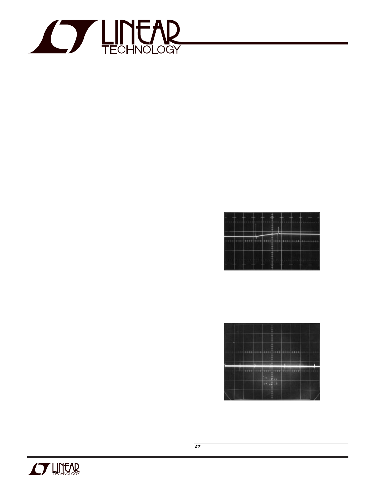
directly related to the regulator’s switching.1 Figure 1
shows typical switching regulator output noise. Two distinct characteristics are present. The slow, ramping output
ripple is caused by finite storage capacity of the regulator’s
output filter components. The quickly rising spikes are
associated with the switching transitions. Figure 2 shows
another switching regulator output. In this case the ripple
has been eliminated by adequate filtering and linear
postregulation, but the wideband spikes remain. It is these
fast spikes that cause so much difficulty in systems. Their
high frequency content often corrupts associated circuitry, degrading performance or even disabling operation. Noise gets into adjacent circuitry via three paths. It is
conducted out of the regulator output lead, it is conducted
back to the driving source (“reflected” noise) and it is
radiated. The multiple transmission paths combine with
the high frequency content to make noise suppression
difficult. Unconscionable amounts of bypass capacitors,
ferrite beads, shields, Mu-metal and aspirin have been
expended in attempts to ameliorate noise-induced effects.
10mV/DIV
(AC COUPLED)
1µs/DIV AN70 F01
Figure 1. Typical Switching Regulator Output “Noise.”
Wideband Spikes Are Difficult to Suppress, Causing System
Interference Problems. Ripple Component Has Low Harmonic
Content, Is Relatively Easily Filtered
20mV/DIV
(AC COUPLED)
Note 1. Noise contains no regularly occurring or coherent components. As such, switching regulator output “noise” is a misnomer.
Unfortunately, undesired switching related components in the
regulated output are almost always referred to as “noise.” As such,
although technically incorrect, this publication treats all undesired
output signals as “noise.” See Appendix B, “Specifying and Measuring
Something Called Noise.”
50µs/DIV AN70 F02
Figure 2. Linear Regulator Eliminates Ripple, but
Wideband Spikes Remain. Peak-to-Peak Amplitude
Exceeds 30mV (Just Visible Near 2nd, 5th and 8th
Vertical Graticule Divisions)
, LTC and LT are registered trademarks of Linear Technology Corporation.
AN70-1
Page 2
Application Note 70
Alternate approaches involve synchronizing switching
regulator operation to the host system or turning off
switching during critical system operation (an “interrupt
driven” power supply). Another approach places critical
system operations between switch cycles, literally running between electronic rain drops.
2
The difficulty of debugging a noise-laden system and the
compromises involved in synchronized approaches could
be eliminated with a low noise switching regulator. An
inherently low noise switching regulator is the most
attractive approach because it eliminates noise concerns
while maintaining system flexibility.
A Noiseless Switching Regulator Approach
The key to an inherently low noise regulator is to minimize
harmonic content in the switching transitions. Slowing
down the switching interval does this, although power
dissipated during the transition causes some efficiency
loss. Reducing switch repetition rate can largely offset the
losses, resulting in a reasonably efficient design with
small magnetics and the desired low noise. Noise reduction by restricting harmonic generation has been
employed before, although the implementations were
complex and narrowly applicable.3 A monolithic approach,
broadly usable over a range of magnetics and applications, is described here.
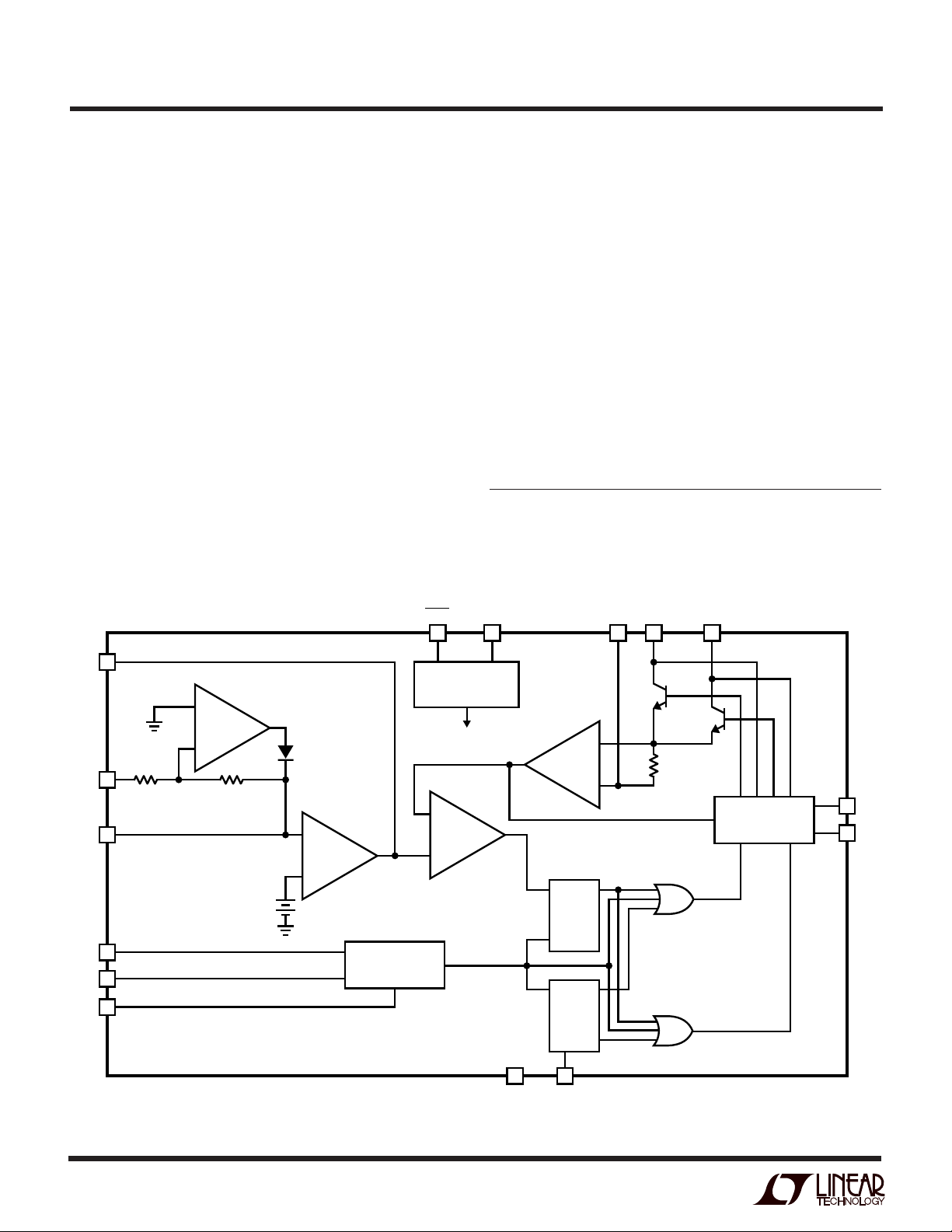
A Practical, Low Noise Monolithic Regulator
Figure 3 describes the LT®1533, a monolithic regulator
designed for low noise switching supplies. Figure 4 details
the pin functions. Figure 3’s functional blocks show a fairly
conventional push-pull architecture with a major exception. The push-pull approach has good magnetics utilization (power transfer is always occurring in the transformer; the core does not store energy) and pulls current
Note 2: See References 2 and 3 for details and practical examples of
these techniques.
Note 3: See Appendix A, “A History of Low Noise DC/DC Conversion.”
See also References 4 through 10.
NFB
SYNC
SHDN V
V
C
LDO REGULATOR
IN
+
NEGATIVE
FEEDBACK
AMP
–
INTERNAL V
CC
CURRENT
PGND COL A COL B
+
AMP
1A
OUTPUT
DRIVERS
–
–
FB
1.25V
R
T
C
T
–
g
m
ERROR
AMP
+
+
OSCILLATOR
+
COMP
SQ
FF
R
Q
T
FF
QB
BK
SLEW CONTROL
R
VSL
R
CSL
Figure 3. LT1533 Simplified Block Diagram. 1A Slew-Controlled Output Stages Provide Low Noise Switching
AN70-2
GND DUTY
AN70 F03
Page 3
Application Note 70
COL A, COL B: Output transistor collectors which switch out-ofphase.
DUTY: Grounding this pin forces the outputs to switch at a 50%
duty cycle. This pin must float if not used.
SYNC: Used to synchronize to an external clock. Float or tie to
ground if unused.
CT: Oscillator timing capacitor.
RT: Oscillator timing resistor.
FB: Used for positive output voltage sensing.
NFB: Used for negative output voltage sensing.
GND: Analog ground pin.
PGND: High current ground return. Should be returned to
ground via ≈ 50nH (≅1" of PC trace or wire, or a small ferrite
bead). See Appendix F or schematic (Figures 5 and 26) notes for
details. In some package options, this pin may be internally
connected to “GND” pin.
VC: Frequency compensation node.
SHDN: Normally high. Grounding this pin shuts the part down.
I
= 20µA.
SHDN
R
: Current slew control resistor.
CSL
R
: Voltage slew control resistor.
VSL
VIN: Input supply pin. 2.7V to 30V range. Undervoltage lockout
at 2.55V.
Figure 4. LT1533 Short Form Pin Function Descriptions
continuously from the source. The even, continuous current drain from the source eliminates the fast, high peak
currents required by flyback and other approaches. The
source sees a benign load and is not corrupted. The
switches also receive nonoverlapping drive, ensuring they
do not conduct simultaneously. Simultaneous conduction
would cause excessive, quickly rising currents, degrading
efficiency and generating noise.
The design’s most significant aspect is the output stage.
Each 1A power transistor operates inside a broadband
control loop. The voltage across each transistor and the
current through it are sensed and the loop controls slew
rate of each parameter. The voltage and current slew rates
are independently settable by external programming
resistors. This ability to control the switching’s rate-ofchange makes low noise switching regulation practical.
Operating the switching transistors in a local loop permits
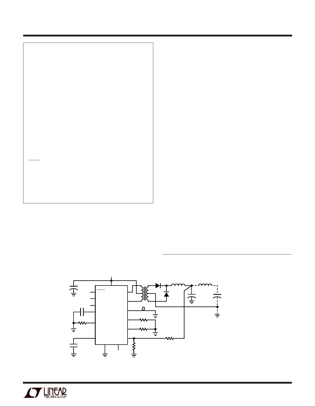
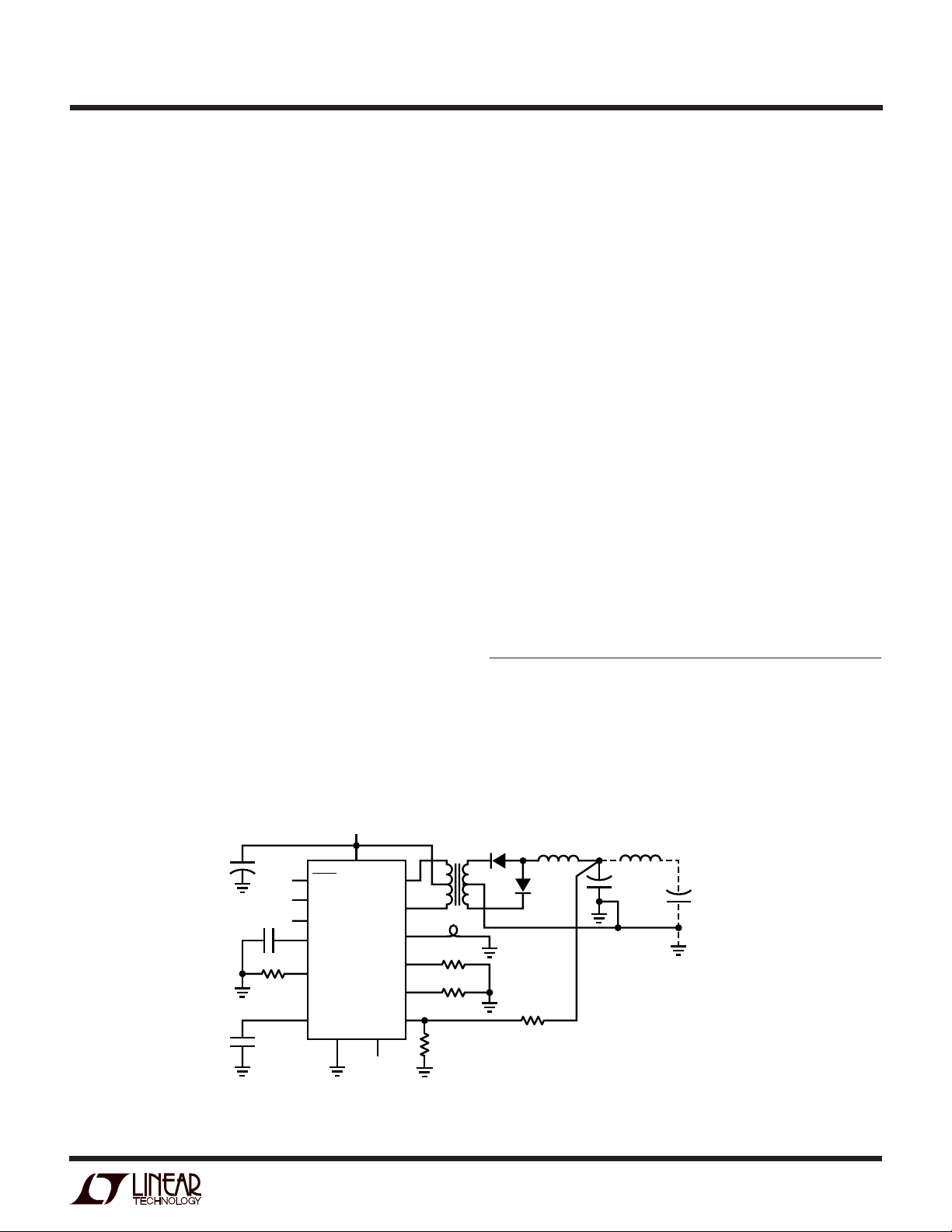
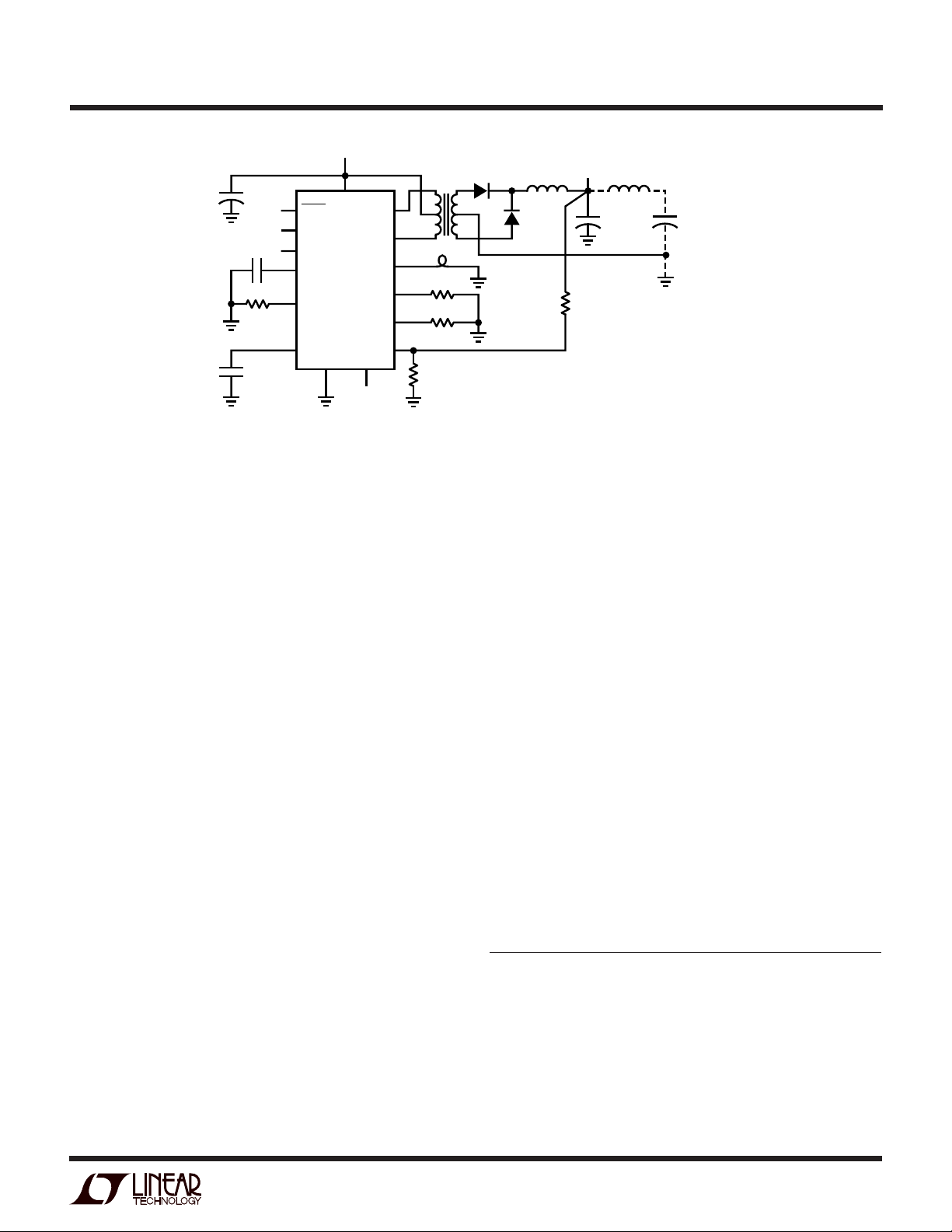
predictable, wide range control over a variety of situations.4 Figure 5 is a 40kHz, 5V to 12V converter using the
LT1533 in a push-pull, “forward” configuration. The feedback resistor’s ratio produces a 12V output. A two-section
LC filter provides high ripple attenuation, although a single
section will give good performance. It is particularly
noteworthy that high frequency noise content (as opposed
to the 40kHz fundamental related ripple) is unaffected by
output filter characteristics. This is so simply because
there is so little high frequency energy developed in this
circuit. If there’s nothing there, it doesn’t need to be
filtered!
L2 provides compensation for the output current control
loop. In practice, L2 may be a length of PC trace, a small
inductor, a coiled section of wire or a ferrite bead. See
Appendix F, “Magnetics Considerations” for complete
discussion.
Note 4: Patent pending.
L3
+
AN70 F05
100µH
OPTIONAL
(SEE TEXT)
C3
47µF
12V
+
47µF
5V
1N4148
+
4.7µF
11
SHDN
3
DUTY
4
3300pF
18k
0.01µF
SYNC
5
C
6
R
10
V
14
V
IN
COL A
COL B
LT1533
PGND
NFB
R
VSL
R
CSL
FB
89
T
T
C
GND
T1
2
15
L2
16
15k
13
15k
12
7
R2
2.49k
1%
L1, L3: COILTRONICS CTX100-3
L2: 22nH TRACE INDUCTANCE, FERRITE BEAD OR
T1: CTX02-13665-X1 (SEE APPENDIX F FOR DETAILS)
L1
100µH
1N4148
R1
21.5k
1%
INDUCTOR (SEE APPENDIX F) COILCRAFT B-07T TYPICAL
Figure 5. 100µV Noise 5V-to-12V Converter. Output LC Section May
Be Deleted If Low Frequency Ripple Is Acceptable
AN70-3
Page 4
Application Note 70
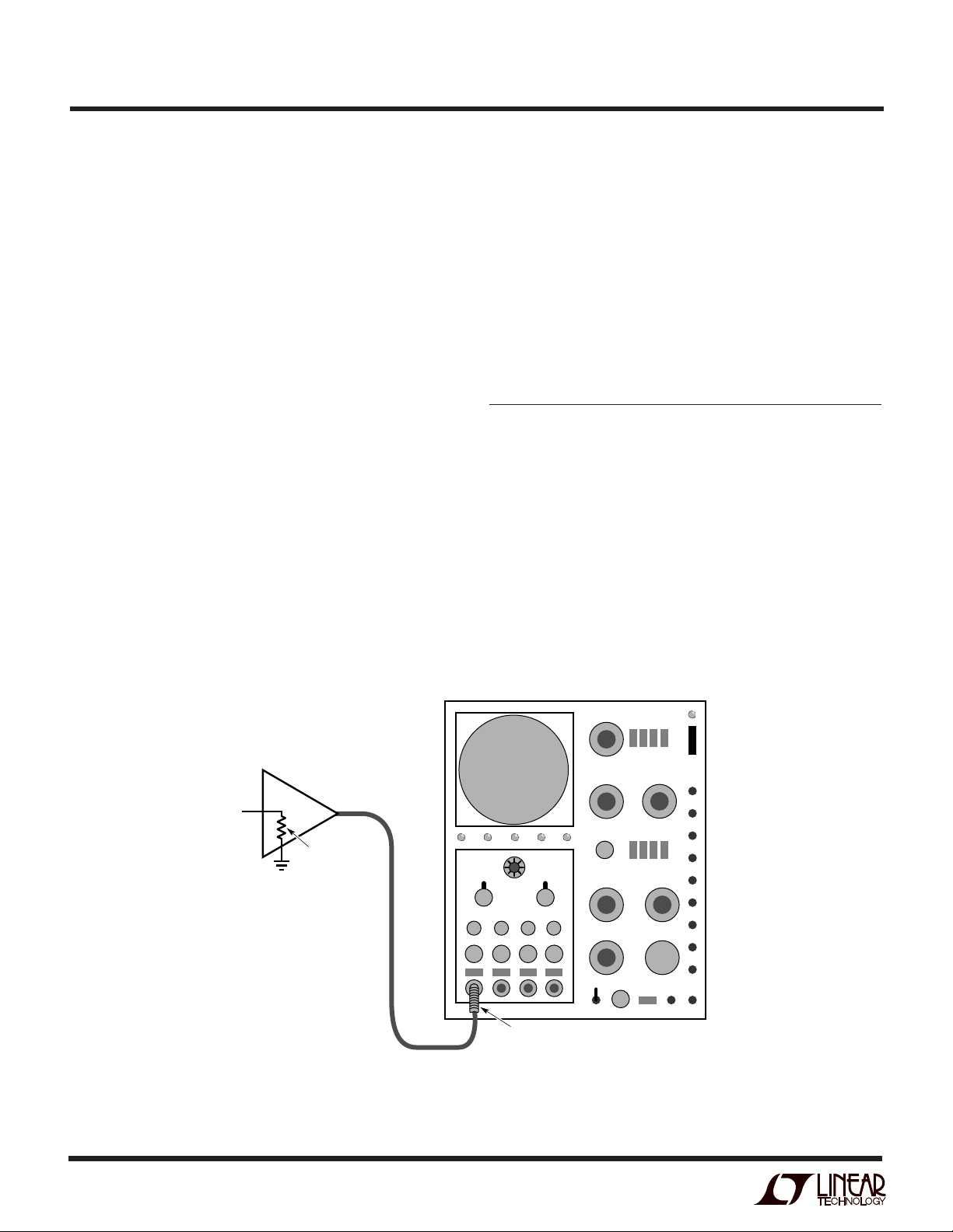
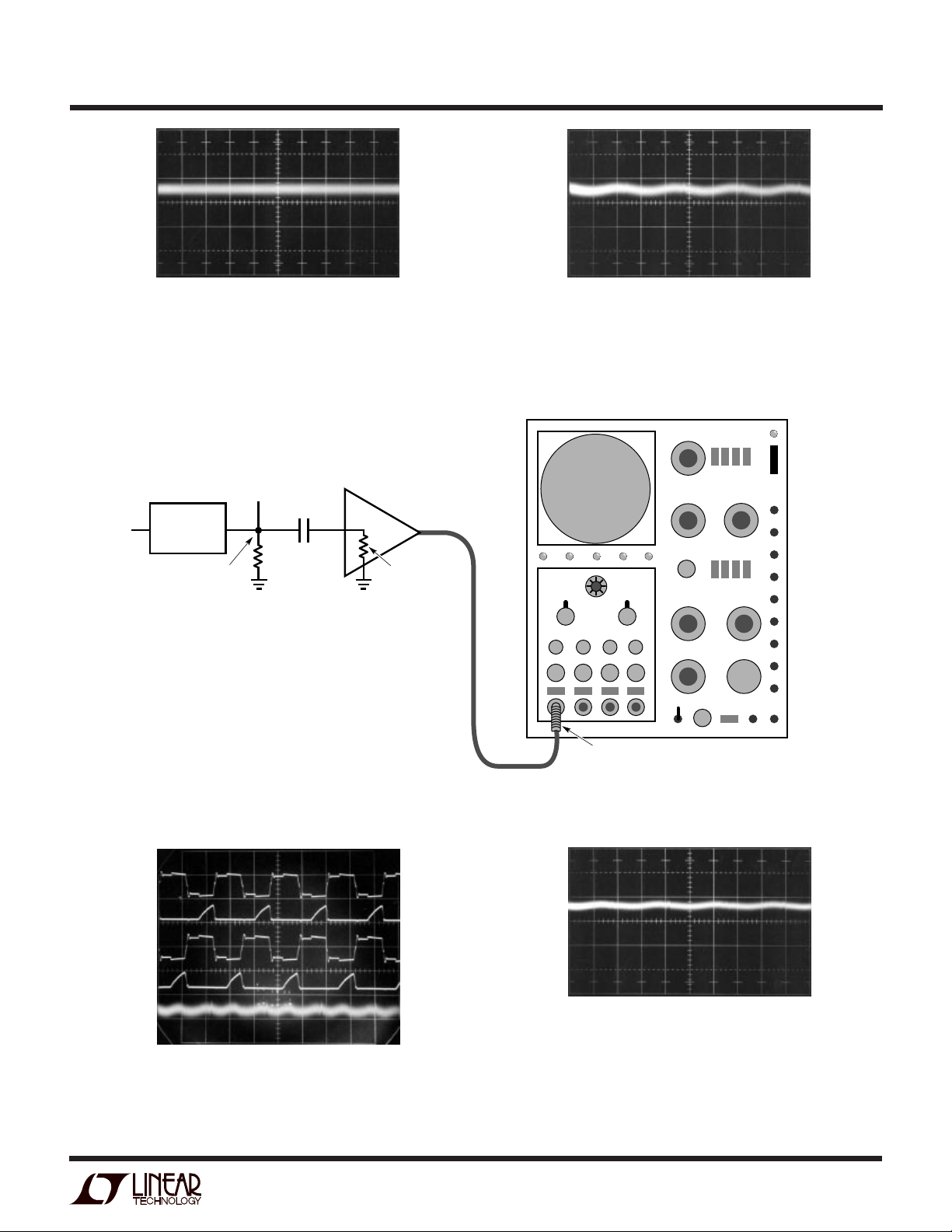
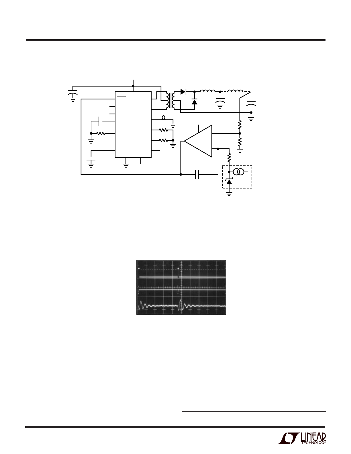
Measuring Output Noise
Measuring the LT1533’s unprecedented low noise levels
requires care.5 Figure 6 shows a test setup for taking the
measurement. Good connection and signal handling technique combined with judicious instrumentation choice
should yield a 100µ V noise floor in a 100MHz bandwidth.
This corresponds to the noise of a 50Ω resistor in a
100MHz bandwidth.
Before measuring regulator output noise, it is good practice to verify test setup performance. This is done by
running the test setup with no input. Figure 7 shows a
noise base line of 100µ V in a 100MHz bandwidth, indicating the instrumentation is operating properly. Measuring
Figure 5’s noise involves AC coupling the circuit’s output
into the test setup’s input. Figure 8 shows this. Coaxial
connections must be maintained to preserve measurement integrity.6 Figure 9’s waveforms detail circuit operation. Traces A and C are switching transistor collector
voltages, B and D are the respective transistor currents.
The test setup’s output, representing circuit output noise,
is Trace E. Wideband spiking and ripple, just visible in the
noise floor, is inside 100µ V, even in a 100MHz bandpass.
7
This is spectacularly good performance and is, in fact,
actually better than the photo shows. Removing all probes
from the breadboard leaves only Trace E’s coaxial connection. This eliminates any possible ground loop-induced
error.8 Figure 10’s trace shows 40kHz ripple with about the
same amplitude as in Figure 9. Switching related spikes,
just faintly outline in the noise, are reduced.
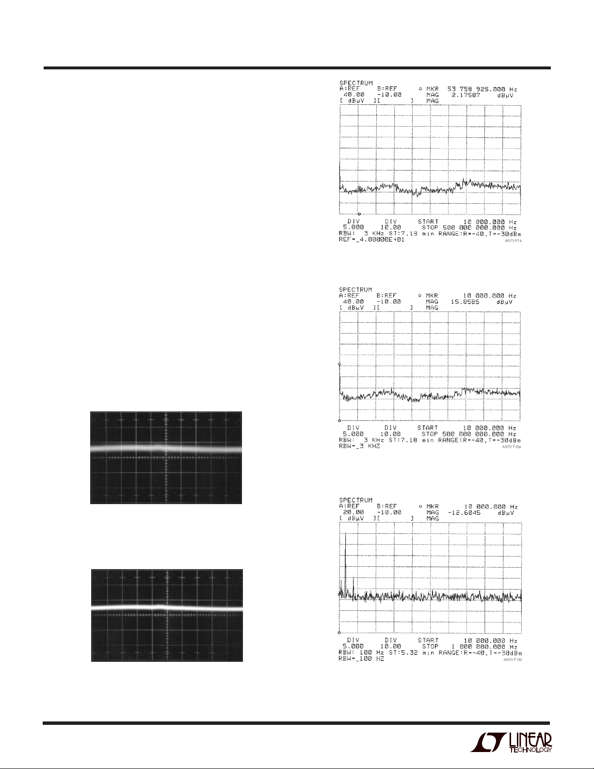
Measurement bandwidth is reduced to 10MHz in Figure
11, attenuating test fixture amplifier noise. Switching and
ripple residue amplitude and shape do not change, indicating no signal activity beyond this frequency. Figure 12’s
Note 5: Equipment selection and measurement techniques are detailed in
Appendix B, “Specifying and Measuring Something Called Noise.” See also
Appendix C, “Probing and Connection Techniques for Low Level,
Wideband Signal Integrity.”
Note 6: Again, see Appendices B and C for extended treatment of these
and related issues.
Note 7: It is common industry practice to specify switching regulator noise
in a 20MHz bandpass. There can be only one reason for this, and it is a
disservice to users. See Appendix B for tutorial on observed noise versus
measurement bandwidth.
Note 8: See Appendix C for related discussion and techniques for
triggering oscilloscopes without invasively probing the circuit.
OSCILLOSCOPE
0.01V/DIV VERTICAL SENSITIVITY
100µV/DIV REFERRED TO AMPLIFIER INPUT
HP461A
AMPLIFIER
X40dB
INPUT
Z
= 50Ω
IN
Figure 6. Test Setup Noise Baseline Is 100µV
50Ω Resistor Noise Limited. BNC Cable Connections and Terminations Provide Coaxial
Environment, Ensuring Wideband, Low Noise Characteristics
BNC
CABLE
50Ω TERMINATOR
HP-11048C OR
EQUIVALENT
in 100MHz Bandwidth. Performance Is
P-P
AN70 F06
AN70-4
Page 5
Application Note 70
100µV/DIV
20µs/DIV AN70 F07
Figure 7. Oscilloscope Verifies Test Setup 100µV Noise Floor in
100MHz Bandwidth. Indicated Noise Is That of a 50Ω Resistor
HP461A
COUPLING
V
OUT
CAPACITOR
SWITCHING
REGULATOR
V
IN
UNDER TEST
BNC CABLE
AND
CONNECTORS
HP-10240B
LOAD
(AS DESIRED)
AMPLIFIER
× 40dB
Z
IN
= 50Ω
100µV/DIV
10µs/DIV
AN70 F07
Figure 10. Removing Probes from Figure 9’s Test Eliminates
Ground Loops, Slightly Reducing Observed Noise. Switching
Artifacts Are Just Discernible Above Noise Floor
OSCILLOSCOPE
0.01V/DIV VERTICAL SENSITIVITY
100µV/DIV REFERRED TO AMPLIFIER INPUT
BNC
CABLE
Figure 8. Connecting Figure 5’s Circuit to the Test Setup. Coaxial Connections Must Be
Maintained to Preserve Measurement Integrity
A = 10V/DIV
B = 1A/DIV
C = 10V/DIV
D = 1A/DIV
E = 100µV/DIV
20µs/DIV AN70 F09
Figure 9. Waveforms for Figure 5 at 100mA Loading. Traces
A and C Are Voltage; B and D are Current, Respectively.
Switching Transistion’s Noise Signature Appears in Trace E,
the Circuit’s Output Noise
100µV/DIV
50Ω TERMINATOR
HP-11048C OR
EQUIVALENT
10µs/DIV AN70 F11
AN70 F08
Figure 11. Reducing Measurement Bandwidth to 10MHz
Attenuates Amplifier Noise. Switching Residue
Characteristics Remain Unchanged, Indicating No Signal
Activity Beyond This Frequency
AN70-5
Page 6
Application Note 70
horizontal expansion of Figure 10 returns to 100MHz
bandpass. The switching spike appears in the center
screen region. At 2µs/division sweep, there is no wide-
band activity observable. Figure 13, a 10MHz bandpass
version of Figure 12, retains all signal information, further
suggesting no signal power beyond 10MHz.
Figure 14 is the noise floor of an HP4195A spectrum
analyzer in a 500MHz sweep. When Figure 5’s circuit is AC
coupled into the analyzer, the output (Figure 15a) is
essentially identical. The analyzer is unable to detect
switching-induced noise in a 500MHz bandpass. Some
40kHz fundamental-related components are detectable in
Figure 15b’s 1MHz wide plot, although the rest of the
sweep is analyzer noise limited. Additional filtering or a
linear postregulator could eliminate the 40kHz ripplerelated residue if desired.
The preamplified oscilloscope is a more sensitive tool for
these measurements because its triggered operation has
the advantage of synchronous detection. This is
demonstratable by free running the preamplified oscilloscope sweep; the switching-related components are
indistinguishable in the noise background.
Figure 14. Noise Floor of Test Fixture and HP-4195A
Spectrum Analyzer in a 500MHz Sweep
100µV/DIV
2µs/DIV AN70 F12
Figure 12. Horizontal Expansion of Figure 10 Shows No
Wideband Components. Switching Originated Noise Appears in
Center Screen Region
100µV/DIV
2µs/DIV AN70F13
Figure 13. A 10MHz Band Limited Version of Figure 12. As Before,
Signal Information Is Retained, Although Amplifier Noise Is
Reduced. Results Indicate No Signal Power Beyond 10MHz
Figure 15a. Figure 5’s Circuit Connected to the Spectrum
Analyzer Produces Essentially Identical Results to Figure
14. Circuit’s Noise Is Undetectable
Figure 15b. Reducing Analyzer Sweep to 1MHz Width
Reveals 40kHz Related Components. Remainder of Plot
Is Analyzer Noise Floor Limited, Even in Sensitive
455kHz Band
AN70-6
Page 7
Figure 16 studies ripple at the first LC filter section output.
The ripple’s 40kHz fundamental is clearly seen, although
no wideband spikes are visible. Figure 17 horizontally
expands Figure 14’s time scale, but high frequency harmonics and spikes are not observable.
Low frequency noise is rarely a concern, although Figure
18 shows it is inside 50µV in a 10Hz to 10kHz bandpass.
Input current noise is usually of more interest. Excessive
“reflected” noise can corrupt the regulator’s driving source,
causing system level interference. Figure 19 shows Figure
5’s input current as DC with a small, 40kHz fundamentalrelated sinusoidal component. There is no high frequency
content, and the sinusoidal variations are easily handled
by the driving source.
System-Based Noise “Measurement”
In the final analysis, the effect of switching regulator
output noise on the system it is powering is the ultimate
test. Appendix K, “System-Based Noise “Measurement,”
presents results when the LT1533 is used to power a
16-bit A/D converter.
Application Note 70
5mV/DIV
10µs/DIV AN70 F16
Figure 16. Ripple at Figure 5’s First LC Output Has No
Wideband Spikes
5mV/DIV
2.5µs/DIV AN70 F17
Figure 17. Time Expansion of Previous Figure. No High
Frequency Content Is Visible
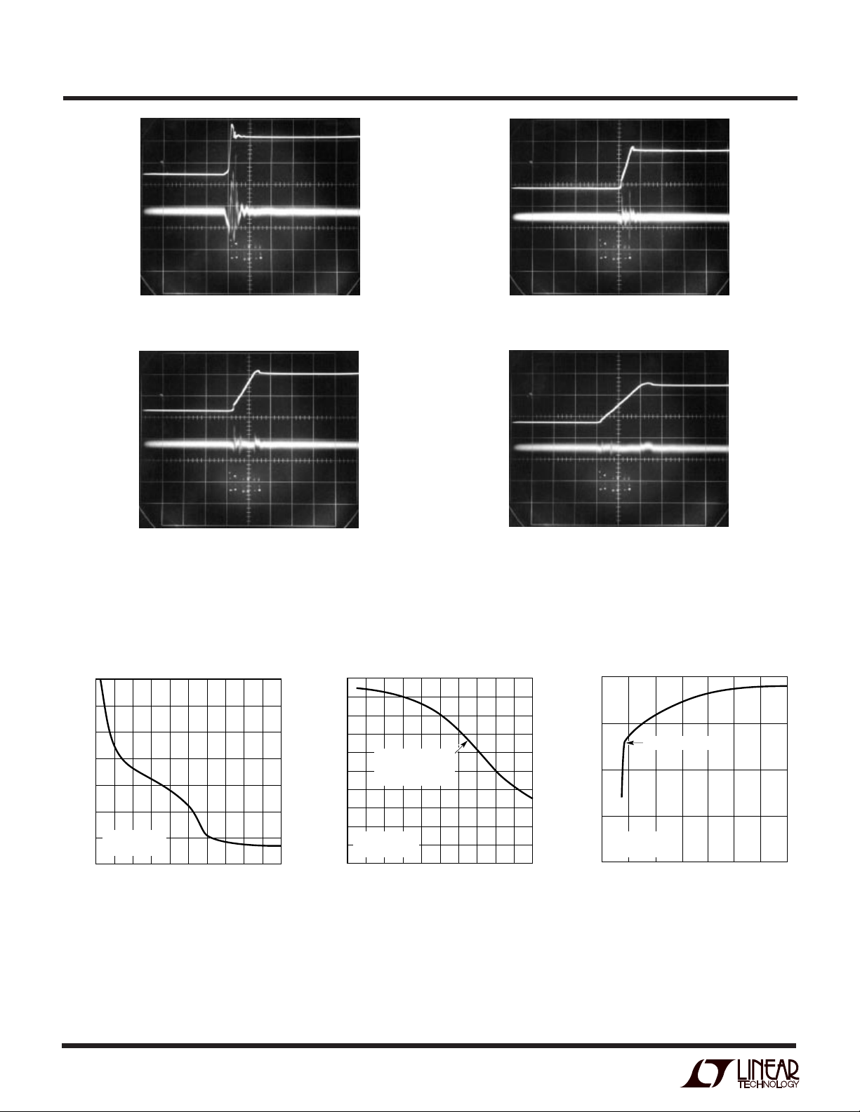
Transition Rate Effects on Noise and Efficiency
In theory, simply setting transition rate to low values will
achieve low noise. Practically, such an approach, while
workable, wastes power during transitions, lowering efficiency. A good compromise sets transition time at the
fastest rate permitting desired noise performance. The
LT1533’s slew adjustments allow easy determination of
this point. Figure 20’s photographs dramatically demonstrate the relationship between transition time and output
noise for Figure 5’s circuit. The sequence shows > 5:1
noise reduction as switch transition time slows from
100ns (20a) to 1µ s (20d). Figure 20d’s displayed noise is
actually lower, as the probing-induced error caused by
monitoring the switch corrupts the measurement.
9
Figure 21 graphically summarizes Figure 20’s information. Significant noise reduction coincides with descending transition slew time until about 1.3µ s. Little additional
noise benefit occurs beyond this point. Figure 22 shows
efficiency fall-off with slew time. There is a 6% penalty
between 100ns and 1.3µs, the same region where noise
performance improves by a factor of 5 (per previous
Note 9: See Appendix C, “Probing and Connection Techniques for Low
Level, Wideband Signal Integrity” for guidance.
50µV/DIV
10ms/DIV
Figure 18. Low Frequency Noise in a 10Hz to 10kHz
Bandpass
10mA/DIV
AC COUPLED
ON 200mA
DC LEVEL
10µs/DIV AN70 F19
Figure 19. Figure 5’s Small Sinusoidal Input Current
Variations Contain No High Frequency Content and Are
Easily Absorbed by Input Supply
AN70 F18
AN70-7
Page 8
Application Note 70
A = 5V/DIV
B = 100µV/DIV
A = 5V/DIV
B = 100µV/DIV
500ns/DIV AN70 F20a
(a)
500ns/DIV AN70 F20a
(c)
A = 5V/DIV
B = 100µV/DIV
500ns/DIV AN70 F20b
(b)
A = 5V/DIV
B = 100µV/DIV
500ns/DIV AN70 F20a
(d)
Figure 20. Output Noise (Trace B) vs Different Switch Slew Rates (Trace A). Highest Slew Rate
(Figure a) Causes Largest Noise. Retarding Slew Rate (Figures b and c) Decreases Noise Until
Lowest Noise Performance Is Achieved (Figure d)
700
600
500
400
300
200
f = 40kHz
100
PEAK-TO-PEAK WIDEBAND NOISE (µV)
= 100mA
I
LOAD
0
0
400
1200 1600
800
SLEW TIME (ns)
2000
AN70 F21
Figure 21. Figure 5’s Noise vs Slew Time
at 40kHz Switching Frequency. Noise
Reduction Beyond 1.3µs Is Minimal
80
78
76
74
72
70
68
EFFICIENCY (%)
66
64
62
60
1.3µs SLEW TIME =
f = 40kHz
= 100mA
I
LOAD
0
400
<100µV NOISE
(SEE FIGURE 21)
800
SLEW TIME (ns)
1200 1600
2000
AN70 F22
Figure 22. Figure 5’s Efficiency Drops 6%
as Slew Time Extends to 1.3µs. Operation
Beyond This Point Gains Little Noise
Performance (See Previous Curve) with
6% Efficiency Penalty
80
75
1.3µs SLEW TIME
70
EFFICIENCY (%)
65
f = 40kHz
= 100mA
I
LOAD
60
100 200 300 400 700
0
WIDEBAND PEAK-TO-PEAK NOISE (µV)
500 600
AN70 F23
Figure 23. Efficiency vs Noise for Figure
5. Data Shows Significant Efficiency FallOff for Noise Below 80µV
AN70-8
Page 9
Application Note 70
figure). There is an additional 6% penalty beyond 1.3µs,
although no significant noise reduction occurs (again, per
Figure 21). As such, operation in this region is undesirable.
Figure 23 clearly shows the inflection point in the efficiency versus noise trade-off.
10
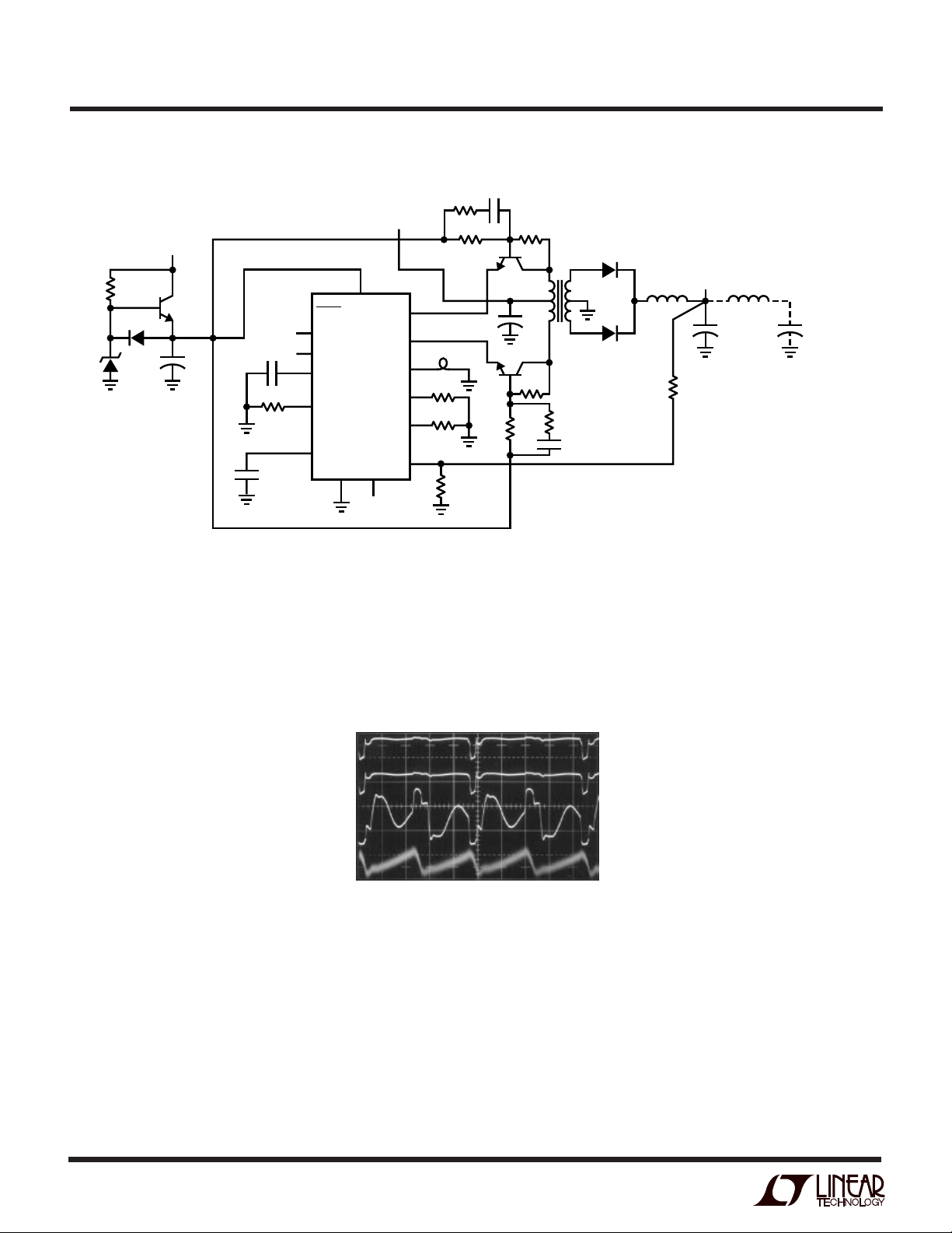
Negative Output Regulator
The LT1533 has a separate feedback input that directly
accepts negative inputs.11 This permits negative outputs
without the usual discrete level shifting stage. Figure 24’s
5V to –12V converter is similar to Figure 5’s circuit, except
that the negative output is fed back to the negative feedback input. The feedback scale factor change is necessitated by the higher effective reference voltage. In all other
respects, the circuit (and its performance) is similar to
Figure 5.
Floating Output Regulator
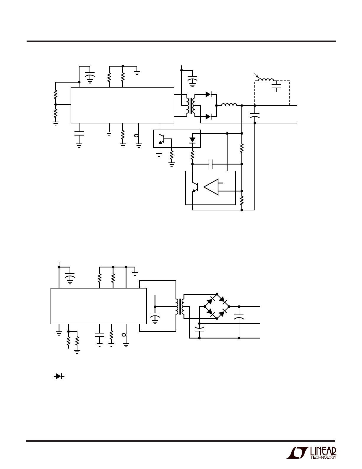
Figure 25’s isolation stage permits a fully floating, regulated output. The LT1431 shunt regulator compares a
portion of the output to its internal reference and drives the
optoisolator with the error signal. The optoisolator’s collector output biases the LT1431’s VC pin, closing a feedback loop to regulate circuit output. The 0.22µ F capacitor
stabilizes the loop and the 240kΩ resistor biases the
optoisolator into a favorable operating region. This circuit’s
operation and characteristics are similar to Figure 5 with
the added benefit of the isolated output.
5V
+
4.7µF
11
SHDN
3
DUTY
4
3300pF
18k
0.01µF
SYNC
5
C
6
R
10
V
14
V
IN
COL A
COL B
LT1533
PGND
R
R
NFB
FB
89
VSL
CSL
T
T
C
GND
T1
2
15
L1
16
15k
13
15k
12
7
R2
2.4k
1%
Floating Bipolar Output Converter
Grounding the LT1533’s “DUTY” pin and biasing FB forces
the device into its 50% duty cycle mode. Figure 26’s output
is full wave rectified with respect to T1’s secondary center
tap, producing bipolar outputs. The forced 50% duty cycle
combined with no feedback means the outputs are
unregulated, proportioning to T1’s drive voltage. An output inductor is usually not required, as in Figure 5’s
“forward” converter. At the very highest output currents,
some inductance may be necessary to limit inrush current.
If this is not done, the circuit may not start. Typically, linear
regulators provide regulation.
12
Figure 26’s waveforms appear in Figure 27. Collector
voltage (Traces A and C) and current (Traces B and D) are
shown, along with the indicated output noise (Trace E). In
this case linear regulators and an output filter are in use.
In Figure 28 all probes except the coaxial output connection are removed. This eliminates probing induced
parasitics,13 allowing a higher fidelity signal presentation.
Here, the switching residuals are barely detectable in the
noise floor. Removing the optional output filter (Figure 29)
allows linear regulator contributed noise and switching
spikes to rise, but noise is still below 300µV
Note 10: The noise and efficiency characteristics appearing in Figures
20 to 23 were generated at the bench in about ten minutes. All you
CAD modeling types out there might want to think about that.
Note 11: See Figure 3’s Block Diagram.
Note 12: See Appendix E, “Selection Criteria for Linear Regulators.”
Note 13: See Appendix C, “Probing and Connection Techniques for
Low Level, Wideband Signal Integrity,” for relevant discussion.
L3
100µH
+
AN70 F24
OPTIONAL
(SEE TEXT)
C3
47µF
–12V
C4
+
47µF
1N4148
L1: 22nH INDUCTOR. COILCRAFT B-07T TYPICAL,
L2, L3: COILTRONICS CTX100-3
T1: COILTRONICS CTX02-13665-X1 (SEE APPENDIX F)
L2
100µH
1N4148
R1
9.6k
1%
TRACE INDUCTANE OR BEAD (SEE APPENDIX F)
P-P
.
Figure 24. A Negative Output Version of Figure 5. LT1533’s Negative Feedback Input Requires
Minimal Configuration Changes. Noise Performance Is Identical to Positive Output Version
AN70-9
Page 10
Application Note 70
F
+
5V
4.2k
820Ω
L1: 22nH INDUCTOR. COILCRAFT B-07T,
TRACE INDUCTANCE OR BEAD. SEE APPENDIX F
L2: COILTRONICS CTX100-3
T1: COILTRONICS CTX-02-13665-X1. SEE APPENDIX F
V
8
FB
C
4.7µF
IN
T
5961610
3300pF
R
VSL
GND
15k
121314
R
CSL
LT1533
R
T
15k
PGND V
18k
L1
22nH
COL A
COL B
C
2
15
4N28
240k
5V
+
4.7µF
T1
1k
OUT
GND
1N4148
1N4148
0.22µF
LT1431
OPTIONAL SECOND
LC SECTION
(SEE TEXT)
L2
100µH
+V
IN
2.5V
–
FB
+
+
9.5k
1%
2.5k
1%
Figure 25. An Optoisolated Output Variant of Figure 5. Loop Closure to VC Pin Bypasses LT1533
Error Amplifier, Enhancing Loop Stability. Noise Performance is Maintained.
L3
TO OUTPUT
COMMON
47µF
AN70 F25
OUTPUT
12V
OUTPUT
COMMON
5V
+
4.7µF
14 13 12
V
IN
GND FB
3300pF
43k
L1: 22nH INDUCTOR. COILCRAFT B-07T TYPICAL,
PC TRACE, OR FERRITE BEAD. SEE APPENDIX F
T1: COILTRONICS CTX-02-13666-X1. SEE APPENDIX F
10k
5V
: 1N4148
15k
R
VSL
LT1533
C
T
R
CSL
R
T
6 5
18k
15k
32
DUTY
PGND
COL A
COL B
L1
5V
+
151689
4.7µF
T1
17V
+
100µF
100µF
+
TO OPTIONAL
LINEAR REGULATORS
AND/OR LC FILTERS,
TYPICALLY 100µH/47µ
–17V
OUTPUT
COMMON
AN70 F26
Figure 26. A Bipolar, Floating Output Converter. Grounding “DUTY” Pin and Biasing FB Puts Regulator into 50%
Duty Cycle Mode. Floating, Unregulated Outputs Proportion to T1’s Center Tap Voltage. Linear Regulators Are
Optional
AN70-10
Page 11
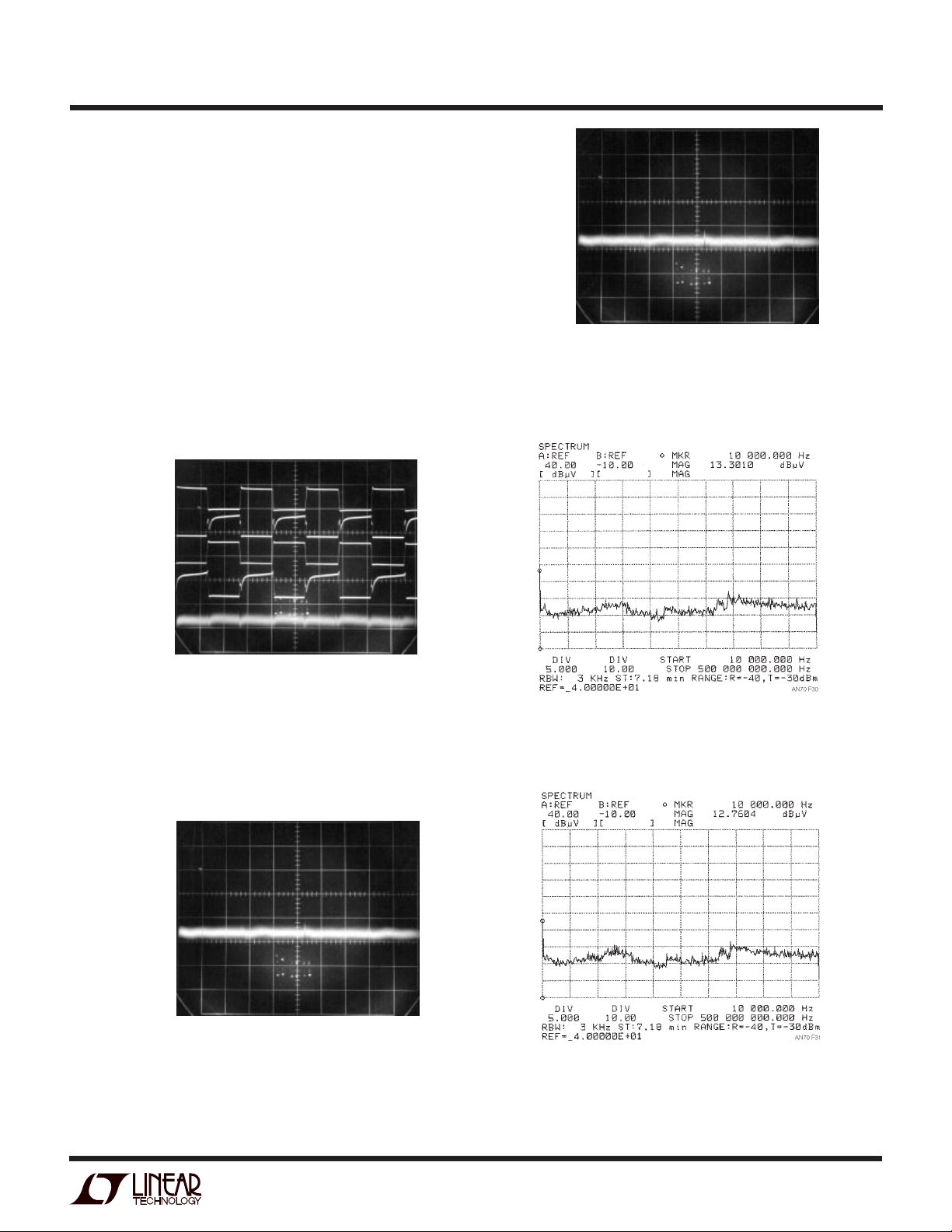
As in Figure 5’s case, spectrum analyzer measurements
are instrument limited. Figure 30 shows the analyzer’s
noise floor in a 500MHz sweep when monitoring the
unpowered Figure 26’s breadboard. In Figure 31, the
breadboard is powered, but analyzer output is noise
limited and essentially indistinguishable from the
unpowered case. Similarly, Figure 32’s 1MHz wide “poweron” plot is identical to Figure 33’s noise floor limited
“power-off” sweep. Note that linear postregulation is in
use and the 40kHz fundamental components are not
detectable. Figure 5’s circuit did not have linear
postregulation and 40kHz fundamental residue appeared
in Figure 15b.
A = 10V/DIV
B = 500mA/DIV
Application Note 70
500µV/DIV
10µs/DIV
Figure 29. Removing Optional LC Filter Causes Linear
Regulator-Contributed Noise and Switching Spikes to Rise.
Peak-to-Peak Noise Is Still <300µV
AN72 F29
C = 10V/DIV
D = 500mA/DIV
E = 100µV/DIV
20µs/DIV
Figure 27. Waveforms for the Floating Output Converter
at 100mA Loading. Linear Postregulator and Optional LC
Filter Are Employed. Slew-Controlled Collector Voltage
(Traces A and C) and Current (Traces B and D) Produce
Output (Trace E) with Under 100µV Noise
100µV/DIV
AN70 F27
Figure 30. HP4195A Analyzer’s Noise Floor in a 500MHz
Sweep When Connected to Unpowered Figure 26
10µs/DIV AN70 F28
Figure 28. Removing All Probes Except Coaxial Output
Connection Reveals Figure 27’s True Noise Figure.
Switching Residue Is Just Detectable in Amplifier Noise
Figure 31. Figure 26’s “Power-On” Output Noise Is
Undetectable in Analyzer’s Noise Floor Limited
500MHz Sweep
AN70-11
Page 12
Application Note 70
Figure 32. Linear Postregulation Eliminates 40kHz
Fundamental-Related Components in 1MHz Sweep
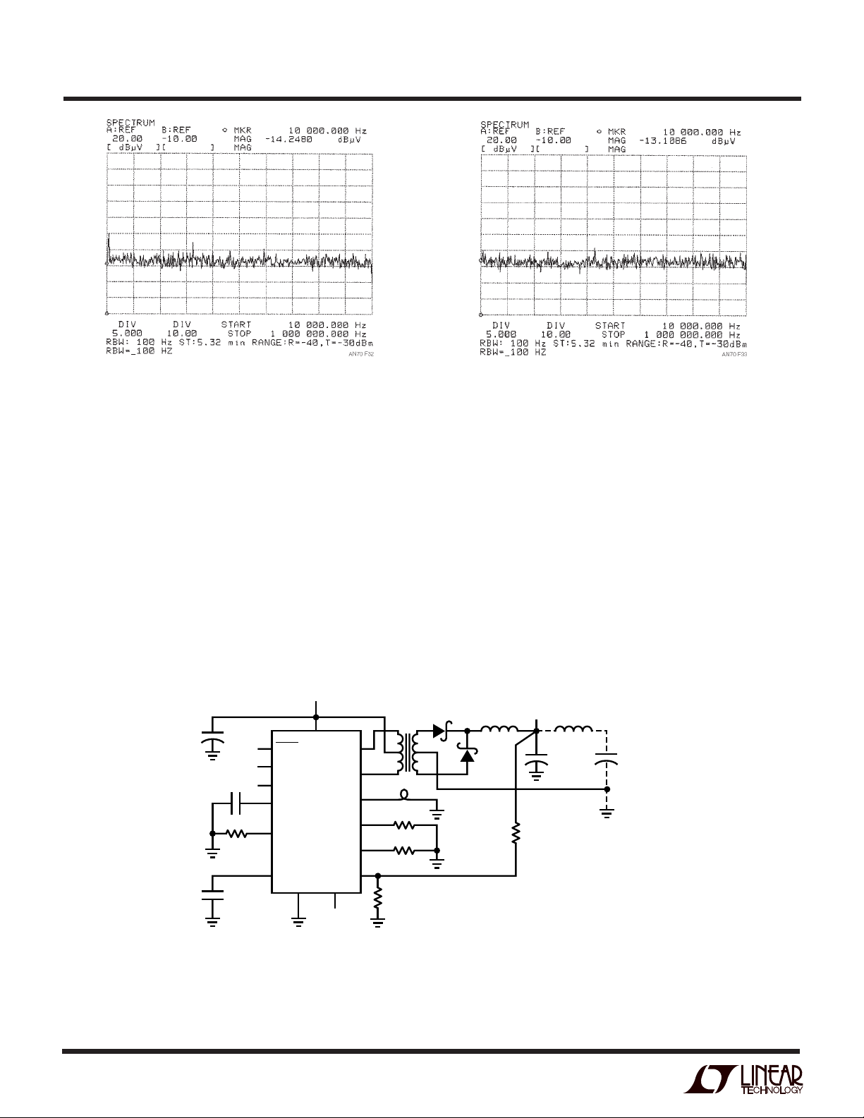
Battery-Powered Circuits
The basic configurations may be battery-powered for use
in portable apparatus. Figure 34, similar to Figure 5, runs
from 2.7V
(e.g., three NiCd batteries), producing 12V
MIN
output. This design induces no noise-based error when
powering a fast 16-bit A/D converter, something almost
no DC/DC converter can do. Appendix K contributes
compelling testimony to this somewhat boastful claim.
2.7V TO 4V
(3 NiCd BATTERIES)
+
4.7µF
11
SHDN
3
DUTY
4
3300pF
18k
0.01µF
SYNC
5
C
6
R
10
V
14
V
IN
COL A
COL B
GND
LT1533
PGND
R
R
NFB
VSL
CSL
FB
89
T
T
C
T1
2
15
L2
16
15k
13
15k
12
7
R2
4.99k
1%
Figure 33. Turning Circuit Power Off Verifies Figure 32’s
Plot Is Analyzer Noise Floor Limited. Sweep Results Are
Identical to Figure 32’s “Power-On” Data
Figure 35 also operates from three NiCd cells, producing
a 9V output. This design achieves 100µV output noise,
qualifying it as the electronic equivalent of a 9V battery.
Performance Augmentation
In some cases it may be desirable to augment LT1533
performance characteristics. Usually, this involves additional circuitry, and may necessitate trading off performance in one area to gain the desired benefit.
L3
L1
1N5817
1N5817
L1, L3: COILTRONICS CTX100-3
L2: 22nH TRACE INDUCTANCE, FERRITE BEAD OR
INDUCTOR (SEE APPENDIX F) COILCRAFT B-07T TYPICAL
T1: CTX02-13665-X1 (SEE APPENDIX F FOR DETAILS)
100µH
5V
+
R1
15k
1%
AN70 F34
OUT
C3
47µF
OPTIONAL FOR
()
100µH
LOWEST RIPPLE
+
47µF
AN70-12
Figure 34. Circuit Delivers 5V from Three NiCd Batteries, Has 100µV Wideband Output
Noise. This Design Contributes No Noise-Based Error When Powering a 16-Bit A/D
Converter (See Appendix K)
Page 13
Application Note 70
2.7V TO 4V
(3 NiCd BATTERIES)
1N4148
+
4.7µF
11
SHDN
3
DUTY
18k
0.01µF
4
SYNC
5
C
6
R
10
V
3300pF
14
V
IN
COL A
COL B
LT1533
PGND
NFB
R
VSL
R
CSL
FB
89
T
T
C
GND
T1
2
15
L2
16
15k
13
15k
12
7
R2
3.48k
1%
L1, L3: COILTRONICS CTX100-3
L2: 22nH TRACE INDUCTANCE, FERRITE BEAD OR
T1: CTX02-13665-X1 (SEE APPENDIX F FOR DETAILS)
L1
9V
100µH
1N4148
R1
21.5k
1%
INDUCTOR (SEE APPENDIX F) COILCRAFT B-07T TYPICAL
Figure 35. Electronic Equivalent of 9V Battery Operates from Three NiCd Cells.
Output Noise Is Below 100µV
OUT
+
AN70 F35
L3
OPTIONAL FOR
()
100µH
LOWEST RIPPLE
C3
47µF
+
47µF
Low Quiescent Current Regulator
The LT1533 has a quiescent current of about 6mA. Figure
36’s circuit reduces this figure to 100µA by running an
on-off control loop around the device. The control loop
replaces the normal error amplifier, achieving regulation
by switching the IC in and out of shutdown in accordance
with loop demands.
Comparator C1 compares a scaled version of the output
with its internal reference and biases the regulators shutdown pin. Loop hysteresis is obtained by utilizing the
phase shift (e.g., time delay) of the output LC components.
In a normal continuously closed loop this phase shift must
be minimized and compensated. In this case it promotes
the desired hysteretic control characteristic. Local AC
positive feedback at C1 ensures clean transitions. Figure
37 shows the loop at work. When circuit output drops
below the regulation point, C1’s output (Trace A) goes
high. This enables the regulator and it responds with a
burst of drive (Trace B) to the transformer. The output is
restored and C1 goes low until the next cycle. During C1’s
low time the regulator is shut down, resulting in the
extremely low quiescent current noted. The loop’s on-off
control characteristic causes low frequency output noise
related to LC tank ring. Trace C shows 600µV peaks,
although no wideband components are observable.
High Voltage Input Regulator
The LT1533’s IC process limits collector breakdown to
30V. A complicating factor is that the transformer swings
to 2× supply. Thus, 15V represents the maximum allowable input supply. Many applications require higher voltage inputs and Figure 38 uses a cascoded14 output stage
to achieve such high voltage capability. This 24V-to-50V
converter is reminiscent of previous circuits, except that
Q1 and Q2 appear. These devices, interposed between the
IC and the transformer, constitute a cascoded high voltage
stage. They provide voltage gain while isolating the IC
from their large collector voltage savings.
Normally, high voltage cascodes are designed to simply
supply voltage isolation. Cascoding the LT1533 presents
special considerations because the transformers instantaneous voltage and current information must be accurately transmitted, albeit at lower amplitude, to the LT1533.
If this is not done, the regulator’s slew control loops will
Note 14: The term “cascode,” derived from “cascade to cathode,” is
applied to a configuration that places active devices in series. The
benefit may be higher breakdown voltage, decreased input capacitance, bandwidth improvement, etc. Cascoding has been employed in
op amps, power supplies, oscilloscopes and other areas to obtain
performance enhancement. The origin of the term is clouded and the
author will mail a magnum of champagne to the first reader correctly
identifying the original author and publication.
AN70-13
Page 14
Application Note 70
(3 Ni-Cd BATTERIES)
+
4.7µF
L1, L3: COILTRONICS CTX100-3
L2: 22nH TRACE INDUCTANCE, FERRITE BEAD OR
T1: CTX02-13665-X1 (SEE APPENDIX F FOR DETAILS)
11
SHDN
3
DUTY
3300pF
4
SYNC
5
C
T
18k
6
R
T
10
V
C
0.01µF
INDUCTOR (SEE APPENDIX F) COILCRAFT B-07T TYPICAL
2.7V TO 4V
V
IN
LT1533
GND
14
COL A
COL B
PGND
R
R
NFB
OPTIONAL
L3
()
SEE TEXT
100µH
12V
C3
47µF
21.5k
1%
150k
+
2.32k
1%
47µF
1.18V
V
INTERNAL
Z
TO LTC1440
AN70 F36
1N4148
5V
C1
LTC1440
10pF
L1
100µH
+
–
+
1N4148
T1
2
15
L2
16
15k
13
VSL
15k
12
CSL
7
FB
89
Figure 36. Hysteretic “Burst ModeTM” Loop Lowers Quiescent
Current to 100µA While Maintaining Low Output Noise
A = 5V/DIV
B = 10V/DIV
C = 500µV/DIV
(10kHz HIGH PASS)
1ms/DIV
AN70 F37
Figure 37. Operating Waveforms for the Low Quiescent Current Converter.
Comparator Output (Trace A) Restores Output Voltage by Turning LT1533
On (Trace B). Output Noise Shows LC Ringing (Trace C), Although High
Frequency Content Is Negligible
AN70-14
Burst Mode is a trademark of Linear Technology Corporation.
Page 15

Application Note 70
not function, causing a dramatic output noise increase.
The AC compensated resistor dividers associated with the
Q1-Q2 base collector biasing serve this purpose. Q3 and
associated components provide a stable DC termination
for the dividers. Figure 39 shows waveforms for Q1’s
operation (Q2 is identical, although of opposing phase).
Trace A is Q1’s emitter, Trace B its base and Trace C the
collector. T1’s ring-off obscures the fact that waveform
fidelity is maintained through the cascode, although inspection reveals this to be the case. Additional testimony
is given by circuit output noise (Trace D), which measures
about 100µV peak.
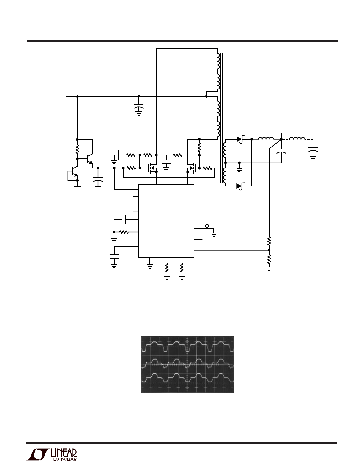
24V-to-5V Low Noise Regulator
Figure 40 extends Figure 38’s cascoding technique in a
step-down design.15 Inputs from 20V to 50V are converted to a 5V/2A capacity output. Q3 and Q4 protect the
regulators VIN pin from the high input voltages. The
cascode must accommodate 100V transformer swings. In
this instance MOSFETs (Q1-Q2) are utilized, although the
divider technique is necessarily retained. RC gate damper
networks prevent transformer swings coupled via gatechannel capacitance from corrupting the cascode’s waveform transfer fidelity. Figure 41 shows that resultant
cascode response is faithful, even with 100V swings.
Trace A is Q1’s source, with Traces B and C its gate and
drain, respectively. Under these conditions, at 2A output,
noise is inside 400µV peak. Note that Q3 and Q4 protect
the regulator from excessive input voltages.
10W, 5V to 12V Low Noise Regulator
Figure 42 boosts the regulator’s 1A output capability to
over 5A. It does this with simple emitter followers (Q1Q2). Theoretically, the followers preserve T1’s voltage and
current waveform information, permitting the LT1533’s
slew control circuitry to function. In practice, the transistors must be relatively low beta types. At 3A collector
current their beta of 20 sources ≈150mA via the Q1-Q2
base paths, adequate for proper slew loop operation.
16
The follower loss limits efficiency to about 68%. Higher
input voltages minimize follower-induced loss, permitting
efficiencies in the low 70% range.
Figure 43 shows noise performance. Ripple measures
4mV (Trace A) using a single LC section, with high
frequency content just discernible. Adding the optional
second LC section drops ripple below 100µV (Trace B),
and high frequency content is seen (note ×50 vertical
scale factor change) to be inside 180µV.
7500V Isolated Low Noise Supply
A final form of performance augmentation is extremely
high voltage isolation. This is often required in situations
where circuitry must withstand high common mode voltage effects. Figure 44 is similar to Figure 25’s isolated
supply, except that it has 7500V (peak) breakdown capability. Transformer and optoisolator changes permit this.
The remaining operating and performance characteristics
are identical to Figure 25.
Note 15: This circuit was developed from a design by Jeff Witt of
Linear Technology Corporation.
Note 16: Operating the slew loops from follower base current was
suggested by Bob Dobkin of Linear Technology Corporation.
AN70-15
Page 16
Application Note 70
24V
10k
3300pF
18k
0.01µF
11
SHDN
3
DUTY
4
SYNC
5
C
T
6
R
T
10
V
C
1N4148
1N752
5.6V
Q3
+
1µF
GND
V
IN
LT1533
9
14
24V
(20V TO 30V)
COL A
COL B
PGND
R
VSL
R
CSL
FB
NFB
8
0.003µF
68Ω
360Ω
2
15
L2
16
15k
13
15k
12
7
R2
2.49k
1%
3.3k
Q1
+
Q2
T1
47µF
3.3k
68Ω
360Ω
L1: COILTRONICS CTX100-3
L2: 22nH TRACE INDUCTANCE, FERRITE BEAD OR
Q1, Q2: ZETEX ZTX-853
Q3: 2N2222A
T1: CTX-02-13665-X1 (SEE APPENDIX F FOR DETAILS)
MUR-110
L1
100µH
50V
OPTIONAL FOR
()
100µH
LOWEST RIPPLE
+ +
47µF
MUR-110
R1
97.6k
1%
0.003µF
INDUCTOR (SEE APPENDIX F) COILCRAFT B-07T TYPICAL
AN70 F38
47µF
Figure 38. A 50V Output Low Noise Regulator. Cascoded Bipolar Transistors Accommodate 60V
Transformer Swings, Permitting 24V (20VIN to 30VIN) Powered Operation
A = 5V/DIV
B = 5V/DIV
C = 20V/DIV
D = 100µV/DIV
1µs/DIV AN70 F39
Figure 39. Cascode Transmits Instantaneous Voltage and Slew
Information, Permitting LT1533 to Maintain Low Noise Output. Trace A
is Q1 Emitter, Trace B Is Its Base and Trace C the Collector.
Transformer Ring-Off Obscures Cascode Action, but Study Reveals
Faithful Transmission. Output (Trace D) Has 100µV Noise
AN70-16
Page 17
Application Note 70
SYNC
DUTY
SHDN
PGND
NFB
FB
R
VSL
R
CSL
LT1533
V
IN
COL A
COL B
14
215
16
8
7
4
3
11
5
6
10
1500pF
0.002µF
17k
0.01µF
0.002µF
L2
10µF
10k
1k
+
L1
100µH
L3
100µH
5V
OUT
13
12
7.5k
1%
2.49k
1%
220µF
MBRS140
L1, L3: COILTRONICS CTX100-3
L2: 22nH TRACE INDUCTANCE, FERRITE BEAD OR
INDUCTOR (SEE APPENDIX F) COILCRAFT B-07T TYPICAL
Q1, Q2: MTD6N15
T1: COILTRONICS VP4-0860
AN70 F40
100µF
C
T
R
T
V
C
OPTIONAL
SEE TEXT
()
+
10k
12k
GND
9
24V
IN
(20V TO 50V)
Q3
MPSA42
Q4
2N2222
4.7µF
10k
9
4
3
10
1
12
2
11
7
6
T1
5
8
Q2
1k
220Ω
10k
220Ω
MBRS140
+
+
Q1
Figure 40. A Low Noise 24V-(20VIN to 50VIN)-to-5V Converter. Cascoded MOSFETs Withstand 100V
Transformer Swings, Permitting LT1533 to Control 5V/2A Output
Figure 41. MOSFET-Based Cascode Permits Regulator to Control 100V Transformer
A = 20V/DIV
B = 5V/DIV
(AC COUPLED)
C = 100V/DIV
10µs/DIV
AN70 F41
Swings While Maintaining Low Noise 5V Output. Trace A Is Q1’s Source, Trace B Q1’s
Gate and Trace C the Drain. Waveform Fidelity Through Cascode Permits Proper Slew
Control Operation
AN70-17
Page 18
Application Note 70
5V
+
4.7µF
11
SHDN
3
DUTY
4
1500pF
18k
0.01µF
SYNC
5
C
6
R
10
V
14
V
IN
T
LT1533
T
C
GND
COL A
COL B
PGND
NFB
2
15
16
L2
10k
13
R
VSL
10k
12
R
CSL
7
FB
89
R2
2.49k
1%
1N4148
330Ω
0.003µF
680Ω
1N5817
1N5817
L1
300µH
AN70 F42
12V
L3
()
33µH
LOWEST RIPPLE
+ +
100µF
OPTIONAL FOR
100µF
0.05Ω
Q1
T1
+
4.7µF
Q2
R1
21.5k
1%
Q1, Q2: MOTOROLA D45C1
0.05Ω
330Ω
1N4148
L1: COILTRONICS CTX300-4
L2: 22nH TRACE INDUCTANCE, FERRITE BEAD OR
INDUCTOR (SEE APPENDIX F) COILCRAFT B-07T TYPICAL
L3: COILTRONICS CTX33-4
T1: COILTRONICS CTX-02-13949-X1
: FERRONICS FERRITE BEAD 21-110J
Figure 42. A 10W Low Noise 5V-to-12V Converter.
Q1-Q2 Provide 5A Output Capacity While Preserving LT1533’s Voltage/Current Slew Control.
Efficiency Is 68%. Higher Input Voltages Minimize Follower Loss, Boosting Efficiency Above 71%
A = 5mV/DIV
B = 100µV/DIV
2µs/DIV
AN70 F41
Figure 43. Waveforms for Figure 42 at 10W Output. Trace A Shows Fundamental
Ripple with Higher Frequency Residue Just Discernible. Optional LC Section
Produces Trace B’s 180µV
Wideband Noise Performance
P-P
AN70-18
Page 19
Application Note 70
+
IN
T
4.7µF
14
R
GND
5
3300pF
5V
4.2k
820Ω
L1: 22nH INDUCTOR. COILCRAFT B-07T,
TRACE INDUCTANCE OR BEAD. SEE APPENDIX F
L2: COILTRONICS CTX100-3
T1: COILTRONICS CTX-02-13950. SEE APPENDIX F
V
5
FB
C
15k
13 12
R
VSL
LT1533
9
R
15k
CSL
T
18k
PGND V
Figure 44. A 7500V Isolation Version of Figure 25.
Transformer and Optoisolator Are Changed to Achieve Isolation
and Noise Immunity. Circuit Operation Is as Before
L1
22nH
C
10166
COL A
COL B
MOC-8112
5V
+
4.7µF
2
15
1N4148
T1
1N4148
1k
OUT
GND
OPTIONAL SECOND
0.22µF
–
+
LT1431
L2
100µH
+V
IN
2.5V
FB
LC SECTION
(SEE TEXT)
9.5k
1%
2.5k
1%
L3
TO OUTPUT
COMMON
+
47µF
AN70 F44
OUTPUT
12V
OUTPUT
COMMON
Note: This Application Note was derived from a manuscript originally
prepared for publication in EDN magazine.
AN70-19
Page 20

Application Note 70
REFERENCES
1. Shakespeare, William, “Much Ado About Nothing,”
II, i, 319, 1598-1600.
2. Williams, Jim, “Design DC/DC Converters to Catch
Noise at the Source,” Electronic Design, October
15, 1981, page 229.
3. Williams, Jim, “Conversion Techniques Adapt
Voltages to Your Needs,” EDN, November 10, 1982,
page 155.
4. Tektronix, Inc. “Type 535 Operating and Service
Manual,” CRT Circuit, 1954.
5. Tektronix, Inc. “Type 454 Operating and Service
Manual,” CRT Circuit, 1967.
6. Tektronix, Inc. “7904 Oscilloscope Operating and
Service Manual,” Converter-Rectifiers, 1972.
7. Hewlett-Packard Co. “1725A Oscilloscope Operating
and Service Manual,” High Voltage Power Supply,
1980.
8. Arthur, Ken, “Power Supply Circuits,” High Voltage
Power Supplies, Tektronix Concept Series, 1967.
9. Williams, Jim and Huffman, Brian, “Some Thoughts
on DC/DC Converters,” Low Noise 5V to ±15V
Converter and Ultralow Noise 5V to ±15V Converter,
pages 1 to 5, Linear Technology Corporation
Application Note 29, 1988.
10. Williams, Jim and Huffman, Brian, “Precise Converter Designs Enhance System Performance,”
EDN, October 13, 1988, pages 175 to 185.
12. Williams, Jim, “High Speed Amplifier Techniques,”
Linear Technology Corporation Application Note 47,
1991.
13. Witt, Jeff, “The LT1533 Heralds a New Class of Low
Noise Switching Regulators,” Linear Technology,
Vol. VII, No. 3, August 1997, Linear Technology
Corporation.
14. Morrison, Ralph, “Noise and Other Interfering
Signals,” John Wiley and Sons, 1992.
15. Morrison, Ralph, “Grounding and Shielding Techniques in Instrumentation,” Wiley-Interscience,
1986.
16. Sheehan, Dan, “Determine Noise of DC/DC Converters,” Electronic Design, September 27, 1973.
17. Hewlett-Packard Co. “HP-11941A Close Field Probe
Operation Note,” 1987.
18. Terrien, Mark, “The HP-11940A Close Field Probe:
Characteristics and Application to EMI Troubleshooting,” RF and Microwave Symposium, available
from Hewlett-Packard Co.
19. Pressman, A.I., “Switching and Linear Power
Supply, Power Converter Design,” Hayden Book
Co., Hasbrouck Heights, New Jersey, 1977.
20. Chryssis, G., “High Frequency Switching Power
Supplies, Theory and Design,” McGraw Hill, New
York, 1984.
11. Tektronix, Inc. “Type 1A7A Differential Amplifier
Instruction Manual,” Check Overall Noise Level
Tangentially, pages 5-36 and 5-37, 1968.
AN70-20
Page 21

APPENDIX A
A HISTORY OF LOW NOISE DC/DC CONVERSION
Application Note 70
Why are batteries low noise power sources? Why do 60Hz
AC power line derived linear regulators have low output
noise? As with most innocent questions, thoughtful
answers provide surprising insights. These sources have
low output noise because they have low harmonic energy
content. A 60Hz fundamental driven supply produces
some harmonic activity, but power becomes very small
well inside 1kHz. A battery is even better.
These conclusions set a direction towards designing low
noise DC/DC converters. If the goal is low noise, the key is
reduction of harmonic energy, in particular, wideband
harmonics. This simple guideline is central to LT1533
operation, although refinements are necessary for a generally applicable IC.
History
The notion of minimizing harmonics in DC/DC conversion
to get low output noise is not new. Oscilloscopes have
used this technique to generate high voltage CRT accelerating potentials without degrading instrument operation.
1
Designing a 10,000V output DC/DC converter that does
not disrupt a 500MHz, high sensitivity vertical amplifier is
challenging.
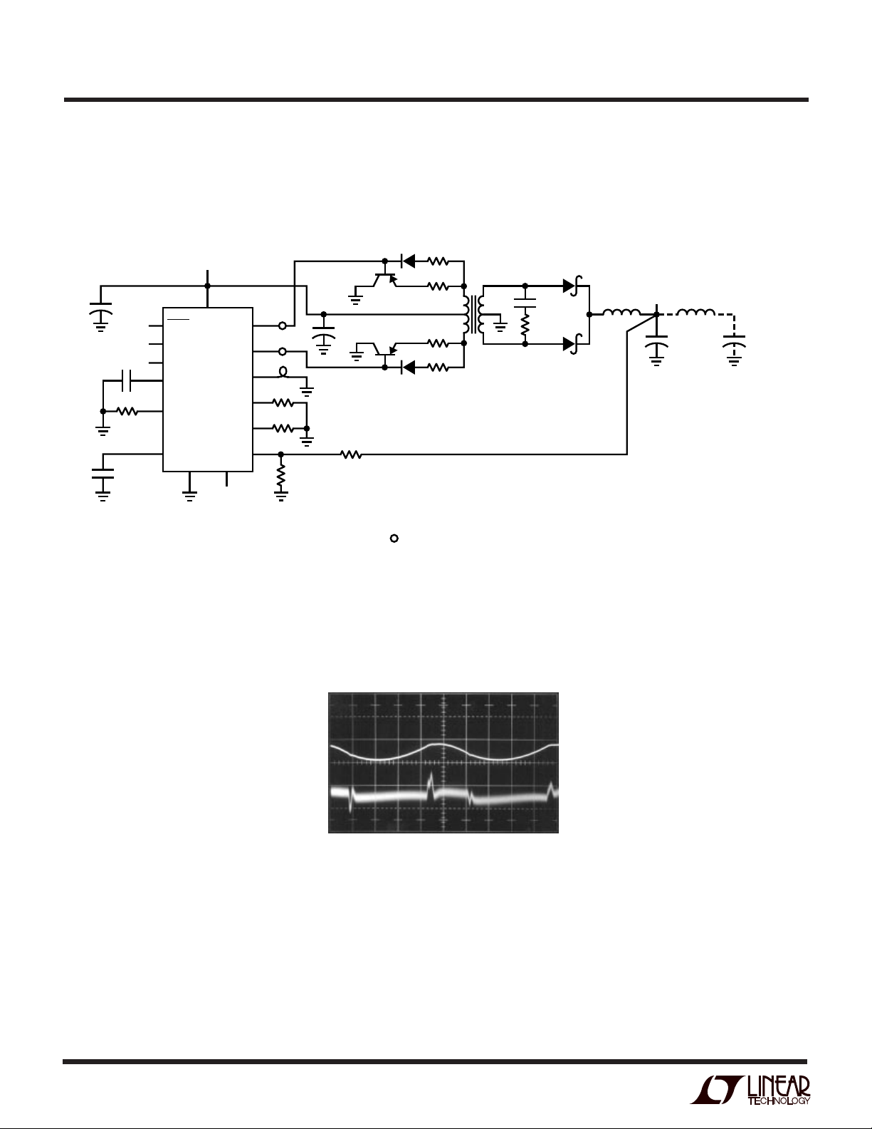
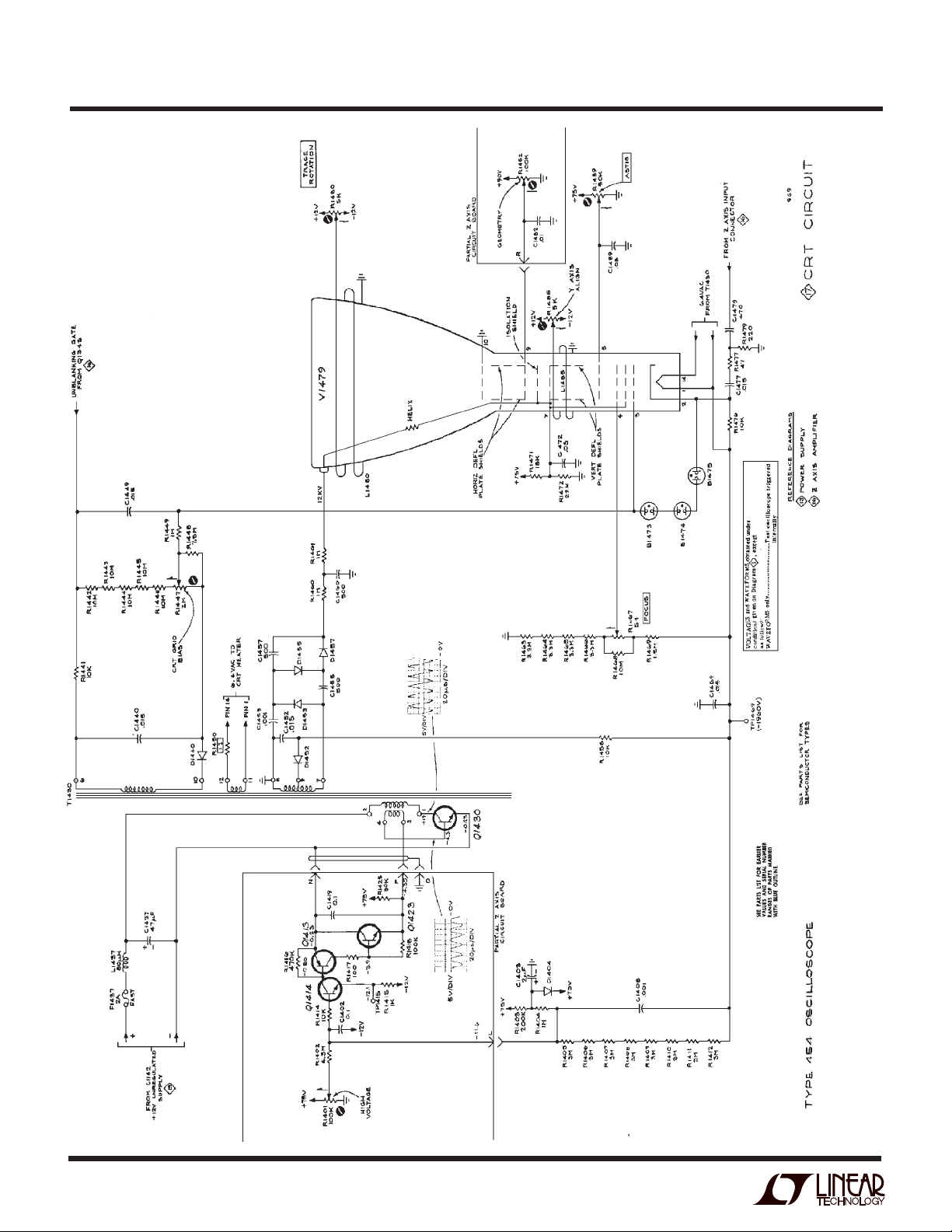
Figure A1 shows the CRT DC/DC converter from a Tektronix
454 oscilloscope. Q1430, configured as a modified Hartley
power oscillator, drives T1430. T1430’s output is multiplied by the diode-capacitor tripler, producing 12,000V.
Feedback to Q1414 is summed against a 75V derived
reference, closing a regulation loop around the power
oscillator.
The sine wave transformer drive (see waveforms in the
figure) has low harmonic content, resulting in the desired
low conducted and radiated noise. This approach is not
very efficient—Q1430 operates in its linear region—but
the power loss is acceptable in a 125W instrument.
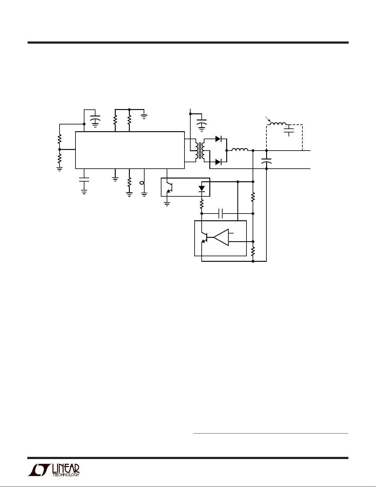
Tektronix 7000 series oscilloscopes used a resonant, offline converter to power the entire instrument. As before,
CRT high voltage was generated separately (see Footnote
1). Figure A2, a partial schematic of a Tektronix 7904
power converter, shows a series resonant network, L1237C1237 in the Q1234-Q1241 drive path. This results in sine
wave drive to output transformer T1310, despite Q1234Q1241’s rectagular waveshape. Feedback (not shown)
closes a loop around this stage, stabilizing its operating
point. The resonant, sine wave transformer drive provides
the desired low noise characteristics with good efficiency.
A less specific example appears in LTC Application Note
29. Figure A3, a partial schematic of Application Note 29’s
Figure 4, shows a sine wave oscillator (A1 based) driving
a power amplifier (A3 and Q2 to Q6). L3, the output
transformer, provides voltage boosted secondary drive to
linear regulators (not shown). This brute force approach
provides a converter with extraordinarily low noise, but is
complex and inefficient. Q4 and Q5, operating in their
linear regions, dissipate considerable power, and efficiency is 30%.
Figure A4’s approach, also from AN29’s Figure 1, achieves
better efficiency. The partial schematic shows source
followers driven from 100Ω-0.003µF edge slow-down
networks. This slows down the transistor’s transitions,
resulting in harmonic reduction and low noise. Unfortunately, the drive scheme is complex and somewhat inflexible, requiring bootstrapped voltages to fully switch the
transistors on and off. Additionally, a transformer change
would require drive rework to maintain efficiency and low
noise characteristics. Finally, the dynamic voltage and
current control in the transistors is passively determined
and not very well controlled.
The LT1533 uses closed-loop control2 around its output
stages to tightly control voltage and current slewing. This
allows a variety of circuits and magnetics to be easily
accommodated, resulting in a true general purpose solution. Text Figure 3 and the associated discussion provide
more LT1533 operating details.
Note 1: Ancillary benefits include eliminating a complex and expensive
high voltage winding in the main power transformer, avoidance of
long, high voltage wire runs and space and weight savings.
Note 2: Patent pending.
AN70-21
Page 22
Application Note 70
Copyright 1967 Tektronix, Inc.
All rights reserved.
Reproduced by permission
AN70-22
Figure A1. Tektronix 454 CRT Circuit Uses Sine Wave Drive for Low Noise DC/DC Conversion.
Efficiency Is Poor, Because Q1430 Remains in Linear Region
Page 23

Application Note 70
Copyright 1972 Tektronix, Inc.
All rights reserved.
Reproduced by permission
Figure A2. Tektronix 7904 Main Inverter Obtains Low Noise by Converting Q1234-Q1241
Rectangular Drive to Sine Wave via L1237-C1237 Resonating Network. Output
Transformer Produces Low Noise Power with Good Efficiency. Approach Is Application
Specific and Inflexible
AN70-23
Page 24

Application Note 70
220Ω
430Ω
8
68Ω
1N4001
1N4001
POWER AMP
50Ω
50Ω
100Ω
0.1Ω
430Ω
+
–
+
–
+
–
+
–
+
A1
LT1006
A3
LT1006
Q5
MJE3055
TO OUTPUT
RECTIFIER/FILTER
AND LINEAR
REGULATION
0.01µF
16kHz
OSCILLATOR
1µF
0.01µF
0.22µF
0.22µF
47µF
Q1
220Ω
680Ω
200k
1k
3.1k
1k
10k
AN70 FA03
20k
10k
1k
1k
1k
8
2k5V820Ω
750Ω
1k
2k
10k
5V
LT1009-2.5
270Ω
(SELECTED VALUE)
1/2
LT1013
A2
OSCILLATOR
STABILITY
LOOP
THERMALLY
MATED
+
10k
Q4
MJE2955
A4
1/2 LT1013
0.22µF
0.1µF
0.1µF
22µF
L4
100µH
5V
IN
4.5V TO 5.5V
0.33µF
620Ω
I
Q
CONTROL
LOOP
+
22µF
+
Q6
Q3
2N2905
Q2
2N2219
330µF
L3
8
1
534
+
Figure A3. Sine Wave-Based DC/DC Converter Appeared in LTC Application Note 29.
Output Noise Is Low, but Circuit Is Complex and Inefficient
AN70-24
Page 25

Application Note 70
22k
0.001µF
CLK
NONOVERLAP
GENERATOR
+
Q1
Q2
POINT “A”
BOOST
OUTPUT
≈17V
0.001µF
0.001µF
100Ω
150k
10k
100Ω
10k
100µF
DC
+
V
Q
74C14
74C14
74C14
FET = MTP3055E
PNP = 2N3906
NPN = 2N3904
L1 = PULSE ENGINEERING, INC. #PE-61592
74C74CLK
D
Q
10k
74C02
10k
74C02
15kHz, 5µs
NONOVERLAP
= ±15V COMMON
= 5V GROUND
= FERRITE BEAD, FERRONICS #21-110J
φ1
φ2
74C14
74C14
LEVEL SHIFTS
1N5817
3
5
Q4
LT1054
BOOST
Q3
1k
DRIVERS
EDGE
SHAPING
100Ω
1k150k
+
100Ω
10µF
2
1N5817
8
+
0.003µF
0.003µF
47µF
Q5
D1
1N5817
+
5V
D
S
1
2
3
S
D
5V
–4V
22µF
AN70 FA4
4
6
7
8
9
L1
OUTPUT
Q6
DC
D3
1N5817
D2
1N5817
TURBO
BOOST
TO OUTPUT
RECTIFIER/FILTER
AND LINEAR
REGULATION
5V
IN
4.5V TO 5.5V
Figure A4. LTC Application Note 29 Circuit Slopes Edge Drive for
Low Noise and Better Efficiency. Gate Drive Circuitry Is Complex
and Poorly Controlled, Making Circuit Inflexible
AN70-25
Page 26

Application Note 70
APPENDIX B
SPECIFYING AND MEASURING SOMETHING CALLED NOISE
Undesired output components in switching regulators
are commonly referred to as “noise.” The rapid, switched
mode power delivery that permits high efficiency conversion also creates wideband harmonic energy. This undesirable energy appears as radiated and conducted components, or “noise.” Actually switching regulator output
“noise” isn’t really noise at all, but coherent, high
frequency residue directly related to the regulator’s switching. Unfortunately, it is almost universal practice to refer
to these parasitics as “noise,” and this publication maintains this common, albeit inaccurate, terminology.
1
Measuring Noise
There are an almost uncountable number of ways to
specify noise in a switching regulator’s output. It is common industrial practice to specify peak-to-peak noise in a
20MHz bandpass.2 Realistically, electronic systems are
readily upset by spectral energy beyond 20MHz, and this
specification restriction benefits no one.3 Considering all
this, it seems appropriate to specify peak-to-peak noise in
a verified 100MHz bandwidth. Reliable low level measurements in this bandpass require careful instrumentation
choice and connection practices.
100µ V of noise. The noise is limited by the amplifier’s 50Ω
noise floor.
4
Figure B4’s presentation of text Figure 5’s output noise
shows barely visible switching artifacts (at vertical graticule lines 4, 6 and 8) in the 100MHz bandpass. Fundamental ripple is seen more clearly, although similarly noise
floor dominated. Restricting measurement bandwidth to
10MHz (Figure B5) reduces noise floor amplitude,
although switching noise and ripple amplitudes are preserved. This indicates that there is no signal power beyond
10MHz. Further measurements as bandwidth is successively reduced can determine the highest frequency content present.
The importance of measurement bandwidth is further
illustrated by Figures B6 to B8. Figure B6 measures a
commercially available DC/DC converter in a 1MHz bandpass. The unit appears to meet its claimed 5mV
P-P
noise
specification. In Figure B7, bandwidth is increased to
10MHz. Spike amplitude enlarges to 6mV
, about 1mV
P-P
outside the specification limit. Figure B8’s 50MHz viewpoint brings an unpleasant surprise. Spikes measure
30mV
—six times the specified limit!
P-P
5
Our study begins by selecting test instrumentation and
verifying its bandwidth and noise. This necessitates the
arrangement shown in Figure B1. Figure B2 diagrams
signal flow. The pulse generator supplies a subnanosecond
rise time step to the attenuator, which produces a <1mV
version of the step. The amplifier takes 40dB of gain
(A = 100) and the oscilloscope displays the result. The
“front-to-back” cascaded bandwidth of this system should
be about 100MHz (t
= 3.5ns) and Figure B3 reveals this
rise
to be so. Figure B3’s trace shows 3.5ns rise time and about
Note 1: Less genteelly, “If you can’t beat ’em, join ’em.”
Note 2: One DC/DC converter manufacturer specifies
20MHz bandwidth. This is beyond deviousness and unworthy of
comment.
Note 3: Except, of course, eager purveyors of power sources who
specify them in this manner.
Note 4: Observed peak-to-peak noise is somewhat affected by the
oscilloscope’s “intensity” setting. Reference 11 describes a method for
normalizing the measurement.
Note 5: Caveat Emptor.
RMS
noise in a
AN70-26
Page 27

Application Note 70
Figure B1. 100MHz Bandwidth Verification Test Setup.
Note Coaxial Connections for Wideband Signal Integrity
AN70-27
Page 28

Application Note 70
100µV/DIV
PULSE
GENERATOR
HP-215A
Z
50Ω
IN
Figure B2. Subnanosecond Pulse Generator and Wideband
Attenuator Provide Fast Step to Verify Test Setup Bandwidth
2ns/DIV AN70B03
ATTENUATOR
HP-355D
1000MHZ<1ns RISE TIME = 350MHz
≈1ns RISETIME
(350MHZ)
<1mV
Z
50Ω
IN
AMPLIFIER
X40dB
HP-461A
150MHZ
= 2.4ns)
(t
r
CASCADED BANDWIDTH ≈ 100MHz
100µV/DIV
50Ω
(≈3.5ns RISE TIME)
OSCILLOSCOPE
TEKTRONIX 454A
150MHZ
(tr = 2.4ns)
AN70 FB2
10µs/DIV AN70 B04
Figure B3. Oscilloscope Display Verifies Test Setup’s
100MHz (3.5ns Rise Time) Bandwidth. Baseline Noise
Derives from Amplifier’s 50Ω Input Noise Floor
100µV/DIV
10µs/DIV AN70 B05
Figure B5. 10MHz Band Limited Version of Preceding
Photo. All Switching Noise Information Is Preserved,
Indicating Adequate Bandwidth
Figure B4. Text Figure 5’s Output Switching Noise Is Just
Discernible in A 100MHz Bandpass
10mV/DIV
50µs/DIV AN70 B06
Figure B6. Commercially Available Switching
Regulator’s Output Noise in a 1MHz Bandpass. Unit
Appears to Meet Its 5mV
Noise Specification
P-P
AN70-28
Page 29

Application Note 70
10mV/DIV
50µs/DIV AN70 B07
Figure B7. Figure A6’s Regulator Noise in a 10MHz Bandpass.
6mV
Noise Exceeds Regulator’s Claimed 5mV Specification
P-P
Low Frequency Noise
Low frequency noise is rarely a concern, because it almost
never affects system operation. Text Figure 5’s low frequency noise is shown in Figure B9. It is possible to reduce
low frequency noise by rolling off control loop bandwidth
(e.g., via a 0.68µF feedback capacitor across R1 and V
C
value of 2000pF in text Figure 5). Figure B10 shows about
a five times improvement when this is done, even with
greater measurement bandwidth. A possible disadvantage is loss of loop bandwidth and slower transient
response.
Preamplifier and Oscilloscope Selection
The low level measurements described require some form
of preamplification for the oscilloscope. Current generation oscilloscopes rarely have greater than 2mV/DIV sensitivity, although older instruments offer more capability.
Figure B11 lists representative preamplifiers and oscilloscope plug-ins suitable for noise measurement. These
20mV/DIV
AN70 B08
50µs/DIV
Figure B8. Wideband Observation of Figure A7 Shows
30mV
Noise—Six Times the Regulator’s Specification!
P-P
units feature wideband, low noise performance. It is
particularly significant that the majority of these instruments are no longer produced. This is in keeping with
current instrumentation trends, which emphasize digital
signal acquisition as opposed to analog measurement
capability.
The monitoring oscilloscope should have adequate bandwidth and exceptional trace clarity. In the latter regard high
quality analog oscilloscopes are unmatched. The exceptionally small spot size of these instruments is well-suited
to low level noise measurement.6 The digitizing uncertainties and raster scan limitations of DSOs impose display
resolution penalties. Many DSO displays will not even
register the small levels of switching-based noise.
Note 6: In our work we have found Tektronix types 454, 454A, 547 and
556 excellent choices. Their pristine trace presentation is ideal for
discerning small signals of interest against a noise floor limited
background.
500µV/DIV 50µV/DIV
10ms/DIV AN70 B09 10ms/DIV AN70 B10
Figure B9. 1Hz to 3kHz Noise Using Standard Frequency
Compensation. Almost All Noise Power Is Below 1kHz
Figure B10. Feedback Lead Network Decreases Low Frequency
Noise, Even as Measurement Bandwidth Expands to 100kHz
AN70-29
Page 30

Application Note 70
INSTRUMENT MODEL MAXIMUM
TYPE MANUFACTURER NUMBER BANDWIDTH SENSITIVITY/GAIN AVAILABILITY COMMENTS
Amplifier Hewlett-Packard 461A 150MHz Gain = 100 Secondary Market 50Ω Input, Stand-Alone
Differential Amplifier Tektronix 1A5 50MHz 1mV/DIV Secondary Market Requires 500 Series Mainframe
Differential Amplifier Tektronix 7A13 100MHz 1mV/DIV Secondary Market Requires 7000 Series Mainframe
Differential Amplifier Tektronix 11A33 150MHz 1mV/DIV Secondary Market Requires 11000 Series Mainframe
Differential Amplifier Tektronix P6046 100MHz 1mV/DIV Secondary Market Stand-Alone
Differential Amplifier Preamble 1855 100MHz Gain = 10 Current Production Stand-Alone, Settable Bandstops
Differential Amplifier Tektronix 1A7/1A7A 1MHz 10µ V/DIV Secondary Market Requires 500 Series Mainframe,
Settable Bandstops
Differential Amplifier Tektronix 7A22 1MHz 10µV/DIV Secondary Market Requires 7000 Series Mainframe,
Settable Bandstops
Differential Amplifier Tektronix 5A22 1MHz 10µV/DIV Secondary Market Requires 5000 Series Mainframe,
Settable Bandstops
Differential Amplifier Tektronix ADA-400A 1MHz 10µV/DIV Current Production Stand-Alone with Optional Power
Supply, Settable Bandstops
Differential Amplifier Preamble 1822 10MHz Gain = 1000 Current Production Stand-Alone, Settable Bandstops
Differential Amplifier Stanford Research SR-560 1MHz Gain = 50000 Current Production Stand-Alone, Settable Bandstops,
Systems Battery or Line Operation
Figure B11. Some Applicable High Sensitivity, Low Noise Amplifiers. Trade-Offs Include Bandwidth, Sensitivity and Availability
APPENDIX C
PROBING AND CONNECTION TECHNIQUES FOR LOW LEVEL, WIDEBAND SIGNAL INTEGRITY
The most carefully prepared breadboard cannot fulfill its
mission if signal connections introduce distortion. Connections to the circuit are crucial for accurate information
extraction. The low level, wideband measurements
demand care in routing signals to test instrumentation.
Ground Loops
Figure C1 shows the effects of a ground loop between
pieces of line-powered test equipment. Small current flow
between test equipment’s nominally grounded chassis
creates 60Hz modulation in the measured circuit output.
This problem can be avoided by grounding all line powered test equipment at the same outlet strip or otherwise
ensuring that all chassis are at the same ground potential.
Similarly, any test arrangement that permits circuit current flow in chassis interconnects must be avoided.
Pickup
Figure C2 also shows 60Hz modulation of the noise
measurement. In this case, a 4-inch voltmeter probe at the
feedback input is the culprit.
connections to the circuit and keep leads short
Minimize the number of test
.
100µV/DIV
Figure C1. Ground Loop Between Pieces of Test
Equipment Induces 60Hz Display Modulation
AN70-30
2ms/DIV AN70 C01
500µV/DIV
5ms/DIV AN70 C02
Figure C2. 60Hz Pickup Due to Excessive
Probe Length at Feedback Node
Page 31

Application Note 70
Figure C3. Poor Probing Technique. Trigger Probe Ground Lead Can
Cause Ground Loop-Induced Artifacts to Appear in Display
AN70-31
Page 32

Application Note 70
Poor Probing Technique
Figure C3’s photograph shows a short ground strap affixed to a scope probe. The probe connects to a point
which provides a trigger signal for the oscilloscope. Circuit output noise is monitored on the oscilloscope via the
coaxial cable shown in the photo.
Figure C4 shows results. A ground loop on the board
between the probe ground strap and the ground referred
cable shield causes apparent excessive ripple in the display.
Minimize the number of test connections to the
circuit and avoid ground loops
100µV/DIV
Figure C4. Apparent Excessive Ripple Results from
Figure C3’s Probe Misuse. Ground Loop on Board
Introduces Serious Measurement Error
.
5µs/DIV AN70 C04
strap is eliminated, replaced by a tip grounding attachment. Figure C8 shows better results over the preceding
case, although signal corruption is still evident.
coaxial connections in the noise signal monitoring path
Maintain
.
Proper Coaxial Connection Path
In Figure C9, a coaxial cable transmits the noise signal to
the amplifier-oscilloscope combination. In theory, this
affords the highest integrity cable signal transmission.
Figure C10’s trace shows this to be true. The former
examples aberrations and excessive noise have disappeared. The switching residuals are now faintly outlined in
the amplifier noise floor.
the noise signal monitoring path
Maintain coaxial connections in
.
Direct Connection Path
A good way to verify there are no cable-based errors is to
eliminate the cable. Figure C11’s approach eliminates all
cable between breadboard, amplifier and oscilloscope.
Figure C12’s presentation is indistinguishable from Figure
C10, indicating no cable-introduced infidelity.
When
results seem optimal, design an experiment to test them.
When results seem poor, design an experiment to test
them. When results are as expected, design an experiment
to test them. When results are unexpected, design an
experiment to test them
.
Violating Coaxial Signal Transmission—Felony Case
In Figure C5, the coaxial cable used to transmit the circuit
output noise to the amplifier-oscilloscope has been
replaced with a probe. A short ground strap is employed
as the probe’s return. The error inducing trigger channel
probe in the previous case has been eliminated; the ’scope
is triggered by a noninvasive, isolated probe.1 Figure C6
shows excessive display noise due to breakup of the
coaxial signal environment. The probe’s ground strap
violates coaxial transmission and the signal is corrupted
by RF.
monitoring path
Maintain coaxial connections in the noise signal
.
Violating Coaxial Signal Transmission—
Misdemeanor Case
Figure C7’s probe connection also violates coaxial signal
flow, but to a less offensive extent. The probe’s ground
Test Lead Connections
In theory, attaching a voltmeter lead to the regulator’s
output should not introduce noise. Figure C13’s increased
noise reading contradicts the theory. The regulator’s output impedance, albeit low, is not zero, especially as
frequency scales up. The RF noise injected by the test lead
works against the finite output impedance, producing the
200µ V of noise indicated in the figure. If a voltmeter lead
must be connected to the output during testing, it should
be done through a 10kΩ-10µF filter. Such a network
eliminates Figure C13’s problem while introducing minimal error in the monitoring DVM.
Minimize the number of
test lead connections to the circuit while checking noise.
Prevent test leads from injecting RF into the test circuit
Note 1: To be discussed. Read on.
.
AN70-32
Page 33

Application Note 70
Figure C5. Floating Trigger Probe Eliminates Ground Loop, but Output Probe
Ground Lead (Photo Upper Right) Violates Coaxial Signal Transmission
500µV/DIV
5µs/DIV AN70 C06
Figure C6. Signal Corruption Due to Figure C5’s
Noncoaxial Probe Connection
AN70-33
Page 34

Application Note 70
AN70-34
Figure C7. Probe with Tip Grounding Attachment Approximates Coaxial Connection
100µV/DIV
5µs/DIV AN70 C08
Figure C8. Probe with Tip Grounding Attachment Improves
Results. Some Corruption Is Still Evident
Page 35

Application Note 70
Figure C9. Coaxial Connection Theoretically Affords Highest Fidelity Signal Transmission
100µV/DIV
5µs/DIV AN70 C10
Figure C10. Life Agrees with Theory. Coaxial Signal
Transmission Maintains Signal Integrity. Switching
Residuals Are Faintly Outlined in Amplifier Noise
AN70-35
Page 36

Application Note 70
Figure C11. Direct Connection to Equipment Eliminates Possible Cable-Termination Parasitics,
Providing Best Possible Signal Transmission
100µV/DIV
5µs/DIV
AN70 C12
Figure C12. Direct Connection to Equipment Provides
Identical Results to Cable-Termination Approach.
Cable and Termination Are Therefore Acceptable
AN70-36
Page 37

Application Note 70
1k
4700pF
L1: J.W. MILLER #100267
AN70 FC14
TERMINATION BOX
SHIELDED
CABLE
L1
PROBE
BNC CONNECTION
TO TERMINATION BOX
DAMPING
ADJUST
BNC
OUTPUT
200µV/DIV
5µs/DIV
AN70 C13
Figure C13. Voltmeter Lead Attached to Regulator Output
Introduces RF Pickup, Multiplying Apparent Noise Floor
Isolated Trigger Probe
The text associated with Figure C5 somewhat cryptically
alluded to an “isolated trigger probe.” Figure C14 reveals
this to be simply an RF choke terminated against ringing.
The choke picks up residual radiated field, generating an
isolated trigger signal. This arrangement furnishes a ’scope
trigger signal with essentially no measurement corruption. The probe’s physical form appears in Figure C15. For
good results the termination should be adjusted for
minimum ringing while preserving the highest possible
amplitude output. Light compensatory damping produces
Figure C16’s output, which will cause poor ’scope triggering. Proper adjustment results in a more favorable output
(Figure C17), characterized by minimal ringing and welldefined edges.
Trigger Probe Amplifier
The field around the switching magnetics is small and may
not be adequate to reliably trigger some oscilloscopes. In
such cases, Figure C18’s trigger probe amplifier is useful.
It uses an adaptive triggering scheme to compensate for
variations in probe output amplitude. A stable 5V trigger
output is maintained over a 50:1 probe output range. A1,
operating at a gain of 100, provides wideband AC gain. The
output of this stage biases a 2-way peak detector (Q1
through Q4). The maximum peak is stored in Q2’s emitter
capacitor, while the minimum excursion is retained in Q4’s
emitter capacitor. The DC value of the midpoint of A1’s
output signal appears at the junction of the 500pF capacitor and the 3MΩ units. This point always sits midway
between the signal’s excursions, regardless of absolute
amplitude. This signal-adaptive voltage is buffered by A2
to set the trigger voltage at the LT1116’s positive input.
The LT1116’s negative input is biased directly from A1’s
output. The LT1116’s output, the circuit’s trigger output,
is unaffected by >50:1 signal amplitude variations. An
X100 analog output is available at A1.
Figure C19 shows the circuit’s digital output (Trace B)
responding to the amplified probe signal at A1 (Trace A).
Figure C20 is a typical noise testing setup. It includes the
breadboard, trigger probe, amplifier, oscilloscope and
coaxial components.
Figure C14. Simple Trigger Probe Eliminates Board
Level Ground Loops. Termination Box Components
Damp L1’s Ringing Response
AN70-37
Page 38

Application Note 70
AN70-38
Figure C15. The Trigger Probe and Termination Box. Clip
Lead Facilitates Mounting Probe, Is Electrically Neutral
Page 39

Application Note 70
(
)
10mV/DIV
10µs/DIV
AN70 C16
Figure C16. Misadjusted Termination Causes
Inadequate Damping. Unstable Oscilloscope
Triggering May Result
5V
+
A1
LT1227
–
750Ω
10µF
2k
5V
+
+
0.1µF
1k
10Ω
100µF
Q1, Q2, Q3, Q4 = CA3096 ARRAY: TIE SUBSTRATE (PIN 16) TO GROUND
0.1µF
= 1N4148
5V
2k
0.005µF
0.005µF
12
6
5
4
10
11
3
1
Q1 Q2
2
13
14
Q3
15
2k
10mV/DIV
10µs/DIV
AN70 C17
Figure C17. Properly Adjusted Termination
Minimizes Ringing with Small Amplitude Penalty
50Ω
3M
500pF
3M
Q4
ANALOG BNC OUTPUT
TO ’SCOPE TRIGGER INPUT
5V
+
A2
LT1006
–
470Ω
0.1µF
470Ω
+
LT1116
–
DIGITAL
TRIGGER
OUT BNC
TO ’SCOPE
AN70 C18
TRIGGER PROBE
AND TERMINATION BOX
SEE FIGURE C14 FOR DETAILS
Figure C18. Trigger Probe Amplifier Has Analog and Digital Outputs. Adaptive
Threshold Maintains Digital Output over 50:1 Probe Signal Variations
A = 1V/DIV
AC COUPLED
B = 5V/DIV
10µs/DIV (UNCALIB) AN70 C19
Figure C19. Trigger Probe Amplifier Analog (Trace A)
and Digital (Trace B) Outputs
AN70-39
Page 40

Application Note 70
AN70-40
Figure C20. Typical Noise Test Setup Includes Trigger Probe,
Amplifier, Oscilloscope and Coaxial Components
Page 41

APPENDIX D
BREADBOARDING AND LAYOUT CONSIDERATIONS
Application Note 70
LT1533-based circuit’s low harmonic content allows their
noise performance to be less layout sensitive than other
switching regulators. However, some degree of prudence
is in order. As in all things, cavalierness is a direct route to
disappointment. Obtaining the absolute lowest noise figure requires care, but performance below 500µ V is readily
achieved. In general, lowest noise is obtained by preventing mixing of ground currents in the return path. Indiscriminate disposition of ground currents into a bus or
ground plane will cause such mixing, raising observed
output noise. The LT1533’s restricted edge rates mitigate
against corrupted ground path-induced problems, but
best noise performance occurs in a “single-point” ground
scheme. Single-point return schemes may be impractical
in production PC boards. In such cases, provide the lowest
possible impedance path to the power entry point from the
inductor associated with the LT1533’s power ground pin.
(Pin 16). Locate the output component ground returns as
close to the circuit load point as possible. Minimize return
current mixing between input and output sections by
restricting such mixing to the smallest possible common
conductive area.
5V to 12V Breadboard
Figure D1 shows text Figure 5’s breadboard. In keeping
with a breadboard’s purpose, it is constructed to be fast
and easy to modify. Single-point returns arrive separately
from the output area (right side of photo) and Pin 16 of the
LT1533 (center left photo). The ground plane carries no
current. The dummy load resistors are
the plane, but returned to the transformer’s center tap. The
center tap and plane are separately tied into the ground
system at the power input common jack.
5V to ±15V Breadboard
Text Figure 24’s breadboard appears in Figure D2. Layout
considerations are similar to Figure D1, although the
design’s floating output mandates changes. The output
load (photo’s right, above BNC connector) returns directly
to the transformer secondary, which floats from input
(and plane) ground potential. The main ground plane is
tied to input common at the power entry port (left banana
jack). The floating output potentials are referred to a
separate, smaller planed area (photo lower right) which is
tied to the transformer secondary center tap.
Demonstration Board
Figure D3 enticingly portrays an LT1533 demonstration
board. The board’s practical layout is readily adaptable to
production versions. This board is useful for observing
LT1533 performance and as an example of a practical
layout. Noise performance is similar to the text’s breadboards.
not
terminated to
AN70-41
Page 42

Application Note 70
AN70-42
Figure D1. Text Figure 5’s 5V-to-12V Converter Breadboard. Construction Is Easy to Change,
Facilitating Experiments. Note Single-Point Ground Returns. Ground Plane Carries No Current,
Is Tied to Input Common at Board Entry Point (Middle Banana Jack)
Page 43

Application Note 70
Figure D2. Text Figure 26’s Breadboard with Linear Output Regulators. Construction
Encourages Changes and Measurement. Layout Is Similar to Figure D1, Although
Floating Output Necessitates Changes. Separate Planed Area (Photo Center Right)
Maintains Low Impedance Between Output-Related Returns
AN70-43
Page 44

Application Note 70
AN70-44
Figure D3. The Very Civilized LT1533 Demonstration Board
in All Its Comely Splendor
Page 45

APPENDIX E
SELECTION CRITERIA FOR LINEAR REGULATORS
Application Note 70
Some applications, particularly floating output circuits,
may require linear postregulators. Selection criteria
include regulator output accuracy, dropout, ripple rejection and line regulation. Often, short-circuit protection is
not needed because drive circuit output impedance and
current limiting prevent destructive overload. In such
cases, if relatively poor output load regulation and accuracy are acceptable, simple Zener diode-emitter followerbased regulation may suffice. LM78L/ 79L type devices
offer 5% output accuracy and improved line regulation,
although dropout is about 2V—significantly higher than a
simple Zener-emitter follower regulator. Ripple rejection
in LM78L/79L types degrades as they approach dropout,
which is the desirable operating region for best efficiency.
High performance regulators such as the LT1575 (negative) and LT1521 (positive) offer dropout voltages below
0.5V, tight line regulation, 1% accuracy and fully specified
ripple rejection close to dropout.
HIGH VOLTAGE,
FLOATING OUTPUT
SINE WAVE GENERATOR
HP200A TYPICAL
TO 20V
0V
RMS
OUTPUT CAPABILITY
RMS
= MUR110
L1 = COILTRONICS CTX100-4
+
L1
100µH
20µF
“NO L”
“L”
+
20µF
It is usually desirable to operate close to dropout to
maintain good overall efficiency. Because of this, regulator ripple rejection should be tested in this intended
operating region. Additionally, cost, size and performance
trade-offs of various filter components and regulators
should be evaluated to determine the best solution for a
particular application.
Testing Ripple Rejection
Ripple rejection may be tested with Figure E1’s arrangement. The generator should operate over the frequency
range of interest and be capable of supplying the required
output drive. In practice, the generator is set to supply the
regulator input operating voltage at the expected LT1533
switching frequency. Comparison of different regulators
and filter components under varying operating conditions
is easily carried out.
OUTPUT
TO ’SCOPE
AN70 E01
DVM
LINEAR
REGULATOR
UNDER TEST
AMPLIFIER
LOAD
(AS DESIRED)
PREAMBLE
1822 TYPICAL
Figure E1. Ripple Rejection Test Setup for Linear Regulators.
LC Combinations and Regulators May Be Evaluated
AN70-45
Page 46

Application Note 70
AN70-46
Figure E2. Ripple Rejection Test Setup Includes Sine Wave
Generator, Breadboard, Amplifier and Oscilloscope
Page 47

APPENDIX F
MAGNETICS CONSIDERATIONS
Application Note 70
Transformers
The LT1533’s symmetrical “push-pull” drive makes transformer behavior quite predictable. As such, transformers
may usually be specified by indicating the operating frequency, power and desired input/output voltages. Figure
F1 lists the transformers used in the text circuits along
with some of their characteristics. These components,
and variations on them, are available from Coiltronics,
telephone #561-241-7876.
Inductors
Inductors in LT1533 circuits do not have special characteristics. Text Figure 5’s circuit, a “forward” type converter,1
requires
an inductor ahead of its filter capacitor,
although additional LC filtering is optional. Figure 26’s
“50%” mode circuit has no output inductor requirement
NOMINAL
INPUT
VOLTAGE
5V
5V
5V
5V
5V
5V
NOMINAL
OUTPUT VOLTAGE
AFTER LINEAR
REGULATOR
12V
12V
±15V
±15V
12V
12V
OUTPUT
POWER
1.5W
3.0W
1.5W
3.0W
1.5W
10W
unless heavily loaded (see text), although LC sections may
be used for best possible ripple attenuation. In either case,
inductor characteristics are not particularly critical. All
circuits shown in the text use Coiltronics “Octa-Pak” type
toroidal core-based inductors.
The 22nH inductor used in the LT1533’s power ground
return (Pin 16) is mandatory. It may take several forms,
including trace inductance, a small coil of wire, a ferrite
bead or the packaged inductor specified in the schematics.
If coiled wire is employed, five turns of #28 is sufficient. An
equivalent length of PC trace gives similar results. A ferrite
bead (e.g., Ferronics #21-110J or equivalent) with one or
two turns of wire also works well. An example of a
packaged 22nH inductor is the Coilcraft B-07T which is
specified in the test circuits.
Note 1: See References 16 and 17 for basic forward converter theory.
COILTRONICS
PART
NUMBER
CTX-02-13716-X1
CTX-02-13665-X1
CTX-02-13713-X1
CTX-02-13664-X1
CTX-02-13834-X3*
CTX-02-13949-X1
CONNECTION
DIAGRAM
A
A
B
B
A
A
A
2
PRIMARY A
3
4
PRIMARY B
5
= TIED TOGETHER
*= HIGH TURNS RATIO VERSION OF CTX-02-13716-X1.
ACCOMMODATES LOW SUPPLY VOLTAGES OR
HIGH DROPOUT REGULATORS
12
SECTION A
10
9
SECTION B
7
PRIMARY A
PRIMARY B
B
2
3
4
5
12
SECTION A
10
9
SECTION B
7
TIE OUTPUT
COMMON TO
THIS POINT
AN70 FF01
Figure F1. Transformer Types Used in Text Circuits. Variations for
Specific Requirements Are Available from Coiltronics, 561-241-7876
AN70-47
Page 48

Application Note 70
APPENDIX G
WHY VOLTAGE AND CURRENT SLEW CONTROL?
Carl T. Nelson
The LT1533 gives dramatic reduction of high frequency
noise by controlling both voltage and current slew rates in
the switch. This technique also has the advantage of
controlling noise in the other switching regulator components, namely, the catch diode and input and output
capacitors.
Figure G1’s block diagram shows the basic concepts for
slew control. The switch Q1 is driven on and off with
currents I1 and I2 switched via S1. These currents are large
enough to drive the switch at very high slew rates. Actual
slew rates are set by I3 for voltage slew and I4 for current
slew.
During switch turn-on, the collector of Q1 is initially high
and current is zero. Inductor current holds the switch high
until switch current equals inductor current. The first
limiting action occurs as current builds in Q1. Current is
sensed by a fixed gain amplifier A3. The increasing current
generates a current through C2 proportional to switch
current slew rate. This current is compared to I4, and the
difference is amplified by A2, which shunts away all
excess I1 current to control switch current slew rate.
When switch current exceeds inductor current, Q1’s collector would normally fall low at a speed limited only by
diode and switch parasitic capacitance. To control voltage
slew, the current through C1 is compared to I3, and the
difference is amplified by A1 to clamp the base current of
Q1. This stops any further rise in switch current and forces
switch voltage to fall at a controlled rate.
At switch turn-off, current and voltage must be controlled
in the reverse order. Switch S1 is flipped to provide reverse
base drive, and the polarity of I3 and I4 is reversed. Almost
immediately, switch current falls slightly below inductor
current. This would normally cause the switch voltage to
slew up, limited only by diode and switch capacitance.
Here, C1 senses voltage slew and A1 controls switch base
drive to limit switch rise time. Switch current remains
essentially constant during voltage slew.
AN70-48
SWITCH
CONTROL
VOLTAGE SLEW CONTROL CIRCUIT
I
3
V
SLEW
PROGRAMMING
A1
I
1
S1
I
2
ON
OFF
SWITCH
DRIVE
CURRENT
CURRENT SLEW CONTROL CIRCUIT
I
4
V
SLEW
PROGRAMMING
CURRENT
A2
CURRENT
C2
C1
Q1
–
A3
+
AN70 G01
Figure G1. Slew Control Conceptual Block Diagram
Page 49

When switch voltage reaches the level where the catch
diode turns on, switch current would normally drop rapidly, creating fast B field transients around the switch,
diode and output capacitor lines. A3 and C2 come into play
here, sensing the decreasing switch current and controlling the base drive via A2 to force a controlled decrease in
switch, diode and capacitor current.
Application Note 70
VOLTAGE
CURRENT
Figure G2 shows switch, diode and output capacitor
waveforms with controlled switch drive in operation. Note
that current and voltage slew limiting do not occur simultaneously. One must take over when the first is complete.
This requires very fast control circuitry to avoid crossover
glitches that would create noise spikes.
APPENDIX H
HINTS FOR LOWEST NOISE PERFORMANCE
The LT1533’s controlled switching times allow extraordinarily low noise DC/DC conversion with surprisingly little
design effort. Wideband output noise well below 500µ V is
easily achieved. In most situations this level of performance is entirely adequate. Applications requiring the
lowest possible output noise will benefit from special
attention to several areas.
Noise Tweaking
The slew time versus efficiency trace-off discussed in the
text should be weighted towards lowest noise to the extent
tolerable. Typically, slew times beyond 1.3µs result in
“expensive” noise reduction in terms of lost efficiency, but
the benefit is available. The issue is how much power is
expendable to obtain incremental decreases in output
noise. Similarly, the layout techniques discussed in
Appendix D should be reviewed. Rigid adherence to these
guidelines will result in correspondingly lower noise performance. The text’s breadboards were originally constructed to provide the lowest possible noise levels, and
then systematically degraded to test layout sensitivity.
This approach allows experimentation to determine the
best layout without expending fanatical attention to details
that provide essentially no benefit.
The slow edge times greatly minimize radiated EMI, but
experimentation with the component’s physical orienta-
TIME
Figure G2. Switch Voltage and Current
During Turn-On and Turn-Off
AN70 G02
tion can sometimes improve things. Look at the components (yes, literally!) and try and imagine just what their
residual radiated field impinges on. In particular, the
optional output inductor may pick up field radiated by
other magnetics, resulting in increased output noise.
Appropriate physical layout will eliminate this effect, and
experimentation is useful. The EMI probe described in
Appendix J is a useful tool in this pursuit and highly
recommended. Appendix I contributes hints on magnetics-based noise and is similarly recommended.
Capacitors
The filter capacitors used should have low parasitic
impedance. Sanyo OS-CON types are excellent in this
regard and contributed to the performance levels quoted
in the text. Tantalum types are nearly as good. The input
supply bypass capacitor, which should be located directly
at the transformer center tap, needs similarly good characteristics. Aluminum electrolytics are not suitable for any
service in LT1533 circuits.
Damper Network
Some circuits may benefit from a small (e.g., 330Ω1000pF) damper network across the transformer secondary if the absolutely lowest noise is needed. Extremely
small (20µ V to 30µV) excursions can briefly appear during
AN70-49
Page 50

Application Note 70
the switching interval when no energy is coming through
the transformer. These events are so minuscule that they
are barely measurable in the noise floor, but the damper
will eliminate them.
tial that measurement technique be trustworthy. Uncountable hours have been lost chasing “circuit problems” that
in reality are manifestations of poor measurement technique. Please read Appendices B and C before pursuing
solutions to circuit noise that isn’t really there.
Measurement Technique
Strictly speaking, measurement technique is not a way to
obtain lowest noise performance. Realistically, it is essen-
Note 1: I do not wax pedantic here. My guilt in this offense runs deep.
APPENDIX I
PROTECTION AGAINST MAGNETICS NOISE IS KNOWLEDGE AND GOOD COMMON SENSE
Jon Roman—Coiltronics, Inc.
Noise Test Data
For this test I chose four of the most common magnetics
geometries that are currently in production use today.
They are as follows: Pot Core, ER Core, E Core and the
Toroid. The following test data was taken using the methods as described in the following paragraphs. The test
circuit used to determine the amount of noise radiation is
as shown in Figure I1 . The push-pull configuration, power
ratings and turns ratios were chosen to align with the Jim
Williams’ low noise designs presently under study. The
distance chosen for the Sniffer Noise Probe1 was set at
that the noise is shown in millivolts rather than gauss, the
conversion for gauss is:
V
PROBE
(mV
) = 2.88mGauss/µs
P-P
After taking the noise reading for each of the UUT’s under
their full load conditions, the load resistor was removed to
allow for observation of magnetizing flux noise. Then,
using the same measurement techniques, the noise was
measured a second time to determine the difference
between the load noise and the magnetizing noise. The
measured worst-case magnetizing noise is shown in
Figure I3.
0.250 inches from the surface of the core structure. This
distance was chosen as a result of preliminary testing to
allow for a measurable reading on the smallest amount of
Note 1: See Appendix J.
Note 2: See Appendix J.
flux lines coming from the quietest core structure. The
measured worst-case full load noise is shown in Figure I2,
for each of the four geometries chosen for this test. Note
5V INPUT
DRIVE
S1
12V OUTPUT
AT 0.255A, 3W
GEOMETRY FULL LOAD MAGNETIZING
Pot Core 20mV
ER Core 63mV
E Core 488mV
Toroid 860mV
Figure I2. Worst-Case Full Load Noise
1
2
AN70-50
P2
RET
Figure I1. Test Circuit
S2
R1
47Ω
AN72 I1
GEOMETRY FULL LOAD MAGNETIZING
Pot Core 16mV
ER Core 49mV
E Core 95mV
Toroid 91mV
Figure I3. Worst-Case Magnetizing Load Noise
Page 51

Application Note 70
Pot Core
The Pot core tested was as predicted the quietest geometry of the ones tested. Just as expected the “Hot Spot” for
noise was located at the window of the gap where the leads
exit the core. Reference the waveform shown in Figure I4.
Note the top waveform shows the voltage input, the middle
waveform shows the noise as recorded using an amplifier
and the bottom waveform is the current through the UUT.
ER Core
The ER core tested was the surprise of the group with a
much lower noise reading than one would have originally
thought possible. Reference the waveform shown in
Figure I5. Note the top waveform shows the voltage input,
the middle waveform shows the noise as recorded using
an amplifier and the bottom waveform is the current
through the UUT.
Figure I4 Figure I5
AN70-51
Page 52

Application Note 70
Toroid
The Toroid core (Figure I6) tested showed a much higher
electronic noise than was originally expected from a
closed-path geometry. The worst-case noise came from
the top of the core, with the winding placed as evenly on
the core as possible. Note the top waveform shows the
voltage input, the middle waveform shows the noise as
recorded using an amplifier and the bottom waveform is
the current through the UUT.
E Core
The E-core (Figure I7) showed the highest concentration
of noise just above the winding on the top center of the
device. The noise on the surrounding sides was measurable but far below the field that was found directly above
and below the part. Note the top waveform shows the
voltage input, middle waveform shows the noise as
recorded using an amplifier and the bottom waveform is
the current through the UUT.
AN70-52
Figure I6
Figure I7
Page 53

Application Note 70
Summary
Figure I8 is a graph showing the relative difference comparing the full load noise against the magnetizing load
noise. It is recognized that closed core structures such as
toroids in inductors produce less stray (leakage) flux than
open structures like rod cores or bobbin cores. Some
recent products offer “magnetic shields” or tubes of
magnetic material around a bobbin-type core in an attempt
to provide a “magnetic shunt” for the flux to follow. These
structures offer very little reduction in noise because of the
high reluctance in the air gap between the “shield” and the
inner bobbin core. The reluctance in this gap is much
higher than that of the magnetic material. The resultant
leakage flux from the gap can defeat the purpose of the
shield almost entirely! The best approach for reducing
noise in inductors is to use true closed-field geometries,
such as the toroid.
When designing for the lowest possible noise in transformer applications, it is important to observe the effects
mV
900
800
700
600
500
400
300
200
100
0
POT CORE ER CORE
LOAD NOISE
of the load current, as opposed to the magnetizing current.
The preceding test demonstrates that the traditional low
noise structures (toroid) can radiate relatively high amounts
of leakage flux due to the coupling characteristics between
windings. The reflected load currents in both the primary
and the secondary do not affect the magnetizing flux, but
create a magnetic leakage field around the wire, if the
coupling is less than perfect. This is, by definition, leakage
flux. The size and shape of the window area can have an
effect on coupling between windings, as well as the shape
of the flux field emanating from the transformer.
Winding technique also has an effect on coupling and
noise. Multifilar winding, as opposed to layer winding, can
offer better coupling characteristics, which in turn, lowers
noise by lessening leakage flux.
Conclusion
Every
millivolt
E CORE TOROID CORE
MAG NOISE
counts.
Figure I8
APPENDIX J
MEASURING EMI RADIATION
EMI (Electromagnetic Interference) is a form of switching
regulator noise. It is a radiated, as opposed to conducted,
phenomenon. LT1533-based circuits produce low amounts
of EMI for the same reason they minimize conducted
noise—controlled switching times. This appendix, guest
written by Bruce Carsten, describes an excellent tool for
relative EMI measurement and how to use it.1 Carsten’s
methods not only show how to measure relative EMI, but
how to identify and silence its source.
Note 1: Calibrated measurements are discussed in References 14
and 15.
AN70-53
Page 54

Application Note 70
APPLICATION NOTE E101: EMI “SNIFFER” PROBE
Bruce Carsten Associates, Inc.
6410 NW Sisters Place, Corvallis, Oregon 97330
541-745-3935
The EMI Sniffer Probe2 is used with an oscilloscope to
locate and identify magnetic field sources of electromagnetic interference (EMI) in electronic equipment. The
probe consists of a miniature 10 turn pickup coil located
in the end of a small shielded tube, with a BNC connector
provided for connection to a coaxial cable (Figure J1). The
Sniffer Probe output voltage is essentially proportional to
the rate of change of the ambient magnetic field, and thus
to the rate of change of nearby currents.
The principal advantages of the Sniffer Probe over simple
pickup loops are:
1. Spatial resolution of about a millimeter.
2. Relatively high sensitivity for a small coil.
3. A 50Ω source termination to minimize cable reflections
with unterminated scope inputs.
4. Faraday shielding to minimize sensitivity to electric
fields.
The EMI Sniffer Probe was developed to diagnose sources
of EMI in switch mode power converters, but it can also be
used in high speed logic systems and other electronic
equipment.
SOURCES OF EMI
Rapidly changing voltages and currents in electrical and
electronic equipment can easily result in radiated and
conducted noise. Most EMI in switch mode power converters is thus generated during switching transients
when power transistors are turned on or off.
Conventional scope probes can readily be used to see
dynamic voltages, which are the principal sources of
common mode conducted EMI. (High dV/dt can also feed
through poorly designed filters as normal mode voltage
spikes and may radiate fields from a circuit without a
conductive enclosure.)
they are more difficult to shield. These changing magnetic
fields can also induce low impedance voltage transients in
other circuits, resulting in unexpected normal and common mode conducted EMI.
These high dI/dt currents and resultant fields can not be
directly sensed by voltage probes, but are readily detected
and located with the Sniffer Probe. While current probes
can sense currents in discrete conductors and wires, they
are of little use with printed circuit traces or in detecting
dynamic magnetic fields.
PROBE RESPONSE CHARACTERISTICS
The Sniffer Probe is sensitive to magnetic fields only along
the probe axis. This directionality is useful in locating the
paths and sources of high dI/dt currents. The resolution is
usually sufficient to locate which trace on a printed circuit
board, or which lead on a component package, is conducting the EMI generating current.
For “isolated” single conductors or PC traces, the Probe
response is greatest just to either side of the conductor
where the magnetic flux is along with probe axis. (Probe
response may be a little greater with the axis tilted towards
the center of the conductor.) As shown in Figure J2, there
is a sharp response null in the middle of the conductor,
with a 180° phase shift to either side and a decreasing
response with distance. The response will increase on the
inside of a bend where the flux lines are crowded together,
and is reduced on the outside of a bend where the flux lines
spread apart.
When the return current is in an adjacent parallel conductor, the Probe response is greatest between the two
conductors as shown in Figure J3. There will be a sharp
null and phase shift over each conductor, with a lower peak
response outside the conductor pair, again decreasing
with distance.
Dynamic currents produce rapidly changing magnetic
fields which radiate far more easily than electric fields as
AN70-54
Note 2: The EMI Sniffer Probe is available from Bruce Carsten
Associates at the address noted in the title of this appendix.
Page 55

Application Note 70
The response to a trace with a return current on the
opposite side of the board is similar to that of a single
isolated trace, except that the probe response may be
greater with the Probe axis tilted away from the trace. A
“ground plane” below a trace will have a similar effect, as
there will be a counter-flowing “image” current in the
ground plane.
© 1997, Bruce Carsten Associates, Inc. * Approx. 160µ Wire, 1.5mm Coil Dia.
Figure J1. Construction of the EMI “Sniffer Probe” for Locating
and Identifying Magnetic Field Sources of EMI
AN70-55
Page 56

Application Note 70
PROBE
PC TRACE
PCB
PROBE VOLTAGE
Figure J2. Sniffer Probe Response to Current in a
Physically “Isolated” Conductor
PROBE
PC TRACES
PCB
PROBE VOLTAGE
Figure J3. Sniffer Probe Response with
Return Current in a Parallel Conductor
The Probe frequency response to a uniform magnetic field
is shown in Figure J4. Due to large variations in field
strength around a conductor, the Probe should be considered as a qualitative indicator only, with no attempt made
to “calibrate” it. The response fall-off near 300MHz is due
to the pickup coil inductance driving the coax cable
impedance, and the mild resonant peaks (with a 1MΩ
scope termination) at multiples of 80MHz are due to
transmission line reflections.
PRINCIPLES OF PROBE USE
The Sniffer Probe is used with at least a 2-channel scope.
One channel is used to view the noise whose source is to
be located (which may also provide the scope trigger) and
the other channel is used for the Sniffer Probe. The probe
response nulls make it inadvisable to use this scope
channel for triggering.
A third scope trigger channel can be very useful, particularly if it is difficult to trigger on the noise. Transistor drive
waveforms (or their predecessors in the upstream logic)
are ideal for triggering; they are usually stable, and allow
immediate precursors of the noise to be viewed.
Start with the Probe at some distance from the circuit with
the Probe channel at maximum sensitivity. Move the
probe around the circuit, looking for “something happening” in the circuit’s magnetic fields at the same time as the
noise problem. A precise “time domain” correlation between EMI noise transients and internal circuit fields is
fundamental to the diagnostic approach.
As a candidate noise source is located, the Probe is moved
closer while the scope sensitivity is decreased to keep the
probe waveform on-screen. It should be possible to
quickly bring the probe down to the PC board trace (or
wiring) where the probe signal seems to be a maximum.
This may not be near the point of EMI generation, but it
should be near a PC trace or other conductor carrying the
current from the EMI source. This can be verified by
moving the probe back and forth in several directions;
when the appropriate PC trace is crossed at roughly right
angles, the probe output will go through a sharp null over
the trace, with an evident phase reversal in probe voltage
on each side of the trace (as noted above).
This EMI “hot” trace can be followed (like a bloodhound on
the scent trail) to find all or much of the EMI generating
current loop. If the trace is hidden on the back side (or
AN70-56
Page 57

Application Note 70
©1996, Bruce Carsten Associates, Inc.
Figure J4. Typical EMI “Sniffer” Probe Frequency Response Measured with
1.3m (51") of 50Ω Coax to Scope
Upper Traces: 1Meg Scope Input Impedance
Lower Traces: 50Ω Scope Input Impedance
inside) of the board, mark its path with a felt pen and locate
the trace on disassembly, on another board or on the
artwork. From the current path and the timing of the noise
transient, the source of the problem usually becomes
almost self-evident.
Several not-uncommon problems (all of which have been
diagnosed with various versions of the Sniffer Probe) are
discussed here with suggested solutions or fixes.
TYPICAL DI/DT EMI PROBLEMS
Rectifier Reverse Recovery
Reverse recovery of rectifiers is the most common source
of dI/dt-related EMI in power converters; the charge stored
in P-N junction diodes during conduction causes a momentary reverse current flow when the voltage reverses.
This reverse current may stop very quickly (<1ns) in
diodes with a “snap” recovery (more likely in devices with
a PIV rating of less than 200V), or the reverse current may
decay more gradually with a “soft” recovery. Typical
Sniffer Probe waveforms for each type of recovery are
shown in Figure J5.
The sudden change in current creates a rapidly changing
magnetic field, which will both radiate external fields and
induce low impedance voltage spikes in other circuits.
This reverse recovery may “shock” parasitic L-C circuits
into ringing, which will result in oscillatory waveforms
with varying degrees of damping when the diode recovers.
A series R-C damper circuit in parallel with the diode is the
usual solution.
Output rectifiers generally carry the highest currents and
are thus the most prone to this problem, but this is often
recognized and they may be well-snubbed. It is not uncommon for unsnubbed catch or clamp diodes to be
more
of an EMI problem. (The fact that a diode in an R-C-D
snubber may need its
own
R-C snubber is not always self-
evident, for example).
AN70-57
Page 58

Application Note 70
PROBE POINTS
Figure J5. Rectifier Reverse Recovery
Typical Fix: Tightly Coupled R-C Snubber
TYP. PROBE WAVEFORMS:
“SOFT”
REVOVERY
“SNAP”
REVOVERY
The problem can usually be identified by placing the
Sniffer Probe near a rectifier lead. The signal will be
strongest on the inside of a lead bend in an axial package,
or between the anode and cathode leads in a TO-220,
TO-247 or similar type of package, as shown in Figure J5.
Using “softer” recovery diodes is a possible solution and
Schottky diodes are ideal in low voltage applications.
However, it must be recognized that a P-N diode with soft
recovery is also inherently lossy (while a “snap” recovery
is not), as the diode simultaneously develops a reverse
voltage while still conducting current: The fastest possible
diode (lowest recovered charge) with a moderately soft
recovery is usually the best choice. Sometimes a faster,
slightly “snappy” diode with a tightly coupled R-C snubber
works as well or better than a soft but excessively slow
recovery diode.
If significant ringing occurs, a “quick-and-dirty” R-C snubber design approach works fairly well: increasingly large
damper capacitors are placed across the diode until the
ringing frequency is halved. We know that the total ringing
capacity is now quadrupled or that the original ringing
capacity is 1/3 of the added capacity. The damper resistance required is about equal to the capacitive reactance of
the original ringing capacity at the original ringing frequency. The “frequency halving” capacity is then connected in series with the damping resistance and placed
across the diode, as tightly coupled as possible.
Snubber capacitors must have a high pulse current capability and low dielectric loss. Temperature stable (disc or
multilayer) ceramic, silvered mica and some plastic filmfoil capacitors are suitable. Snubber resistors should be
noninductive; metal film, carbon film and carbon composition resistors are good, but wirewound resistors must be
avoided. The maximum snubber resistor dissipation can
be estimated from the product of the damper capacity,
switching frequency and the square of the peak snubber
capacitor voltage.
Snubbers on passive switches (diodes) or active switches
(transistors) should always be coupled as closely as
physically possible, with minimal loop inductance. This
minimizes the radiated field from the change in current
path from the switch to the snubber. It also minimizes the
turn-off voltage overshoot “required” to force the current
to change path through the switch-snubber loop inductance.
AN70-58
Page 59

Application Note 70
Ringing in Clamp Zeners
A capacitor-to-capacitor ringing problem can occur when
a voltage clamping Zener or TransZorb® is placed across
the output of a converter for overvoltage protection (OVP).
Power Zeners have a large junction capacity, and this can
ring in series with the lead ESL and the output capacitors,
with some of the ringing voltage showing up on the output.
This ringing current can be most easily detected near the
Zener leads, particularly on the inside of a bend as shown
in Figure J6.
R-C snubbers have not been found to work well in this case
as the ringing loop inductance is often as low or lower than
the obtainable parasitic inductance in the snubber.
Increasing the external loop inductance to allow damping
is not advisable as this would limit dynamic clamping
capability. In this case, it was found that a small ferrite
bead on one or both of the Zener leads dampened the HF
oscillations with minimal adverse side effects (a high
permeability ferrite bead quickly saturates as soon as the
Zener begins to conduct significant current).
TransZorb is a registered trademark of General Instruments, GSI.
Paralleled Rectifiers
A less evident problem can occur when dual rectifier
diodes in a package are paralleled for increased current
capability, even with a tightly coupled R-C snubber. The
two diodes seldom recover at exactly the same time, which
can cause a very high frequency oscillation (hundreds of
MHz) to occur between the capacities of the two diodes in
series with the anode lead inductances, as shown in Figure
J7. This effect can really only be observed by placing the
probe between the two anode leads, as the ringing current
exists almost nowhere else (the ringing is nearly “invisible” to a conventional voltage probe, like many other EMI
effects that can be easily found with a magnetic field
Sniffer Probe).
This “teeter-totter” oscillation has a voltage “null” about
where the R-C snubber is connected, so it provides little or
no damping (see Figure J7a). It is actually very difficult to
insert a suitable damping resistance into this circuit.
The easiest way to dampen the oscillation is to “slit” the
anode PC trace for an inch or so and place a damping
resistor at the anode leads as shown in Figure J7b. This
PROBE POINTS
TYP. PROBE WAVEFORM:
I
Figure J6. Ringing Between Clamp Zener and Capacitor
Typical Fix: Small Ferrite Bead on Zener Lead(s)
100-500MHz
RINGING
AN70-59
Page 60

Application Note 70
+
Probe Point
(a)
(b)
(C)
Package Lead ESL
Rd
I
RING
PCB Connections
Rd
+
+
Figure J7. Ringing in Paralleled Dual Rectifiers
increases the inductance in series with the diode-diode
loop external to the package and leads, while having
minimal effect on the effective series inductance. Even
better damping is obtained by placing the resistor across
the anode leads at the entry point to the case, as shown in
Figure J7c, but this violates the mindset of many production engineers.
It is also preferable to split the original R-C damper into
two (2R) – (C/2) dampers, one on each side of the dual
rectifier (also shown in Figure 7c). In practice, it is always
preferable to use dual R-C dampers, one each side of the
diode; loop inductance is cut about in half, and the external
dI/dt field is reduced even further due to the oppositely
“handed” currents in the two snubber networks.
Paralleled Snubber or Damper Caps
A problem similar to that with the paralleled diodes occurs
when two or more low loss capacitors are paralleled and
driven with a sudden current change. There is a tendency
for a current to ring between the two capacitors in series
with their lead inductances (or ESL), as shown in Figure
J8a. This type of oscillation can usually be detected by
placing the Sniffer Probe between the leads of the paralleled capacitors. The ringing frequency is much lower than
with the paralleled diodes (due to the larger capacity), and
the effect
may
be benign if the capacitors are sufficiently
close together.
If the resultant ringing is picked up externally, it can be
damped in a similar way as with the parallel diodes as
shown in Figure J8b. In either case, the dissipation in the
damping resistor tends to be relatively small.
AN70-60
Page 61

Probe Point
(a)
Application Note 70
I
RING
(b)
Figure J8. Ringing in Paralleled “Snubber” Capacitors
Ringing in Transformer Shield Leads
The capacity of a transformer shield to other shields or
windings (CS in Figure J9) forms a series resonant circuit
with its “drain wire” inductance (LS) to the bypass point.
This resonant circuit is readily excited by typical square
wave voltages on windings, and a poorly damped oscillatory current may flow in the drain wire. The shield current
may radiate noise into other circuits, and the shield voltage
will often show up as common mode conducted noise. The
shield voltage is very difficult to detect with a voltage probe
in most transformers, but the ringing shield current can be
observed by holding the Sniffer Probe near the shield drain
wire (Figure J10), or the shield current’s return path in the
circuit.
This ringing can be dampened by placing a resistor RD in
series with the shield drain wire, whose value is approximately equal to the surge impedance of the resonant
circuit, which may be calculated from the formula in
Figure J9.
The shield capacitance (CS) can readily be measured with
a bridge (as the capacity from the shield to all facing
shields and/or windings), but LS is usually best calculated
from CS and the ringing frequency (as sensed by the
Sniffer Probe). This resistance is typically on the order of
tens of ohms.
One or more small ferrite beads can also be placed on the
drain wire instead to provide damping. This option may be
preferable as a late “fix” when the PC board has already
been laid out.
Rd
In either case, the damper losses are typically quite small.
The damper resistor has a moderately adverse impact on
shield effectiveness below the shield and drain wire resonant frequency; damper beads are superior in this respect
as their impedance is less at lower frequencies. The drain
wire connection should also be as short as possible to the
circuit bypass point, both to minimize EMI and to raise the
shield’s maximum effective (i.e., resonant) frequency.
Leakage Inductance Fields
Transformer leakage inductance fields emanate from between primary and secondary windings. With a single
primary and secondary, a significant dipole field is created, which may be seen by placing the Sniffer Probe near
the winding ends as shown in Figure J11a. If this field is
generating EMI, there are two principal fixes:
1. Split the Primary or Secondary in two, to “sandwich”
the other winding, and/or:
2. Place a shorted copper strap “electromagnetic shield”
around the
shown in Figure J12. Eddy currents in the shorted strap
largely cancel the external magnetic field.
The first approach creates a “quadrupole” instead of a
dipole leakage field, which significantly reduces the distant field intensity. It also reduces the eddy current losses
in any shorted strap electromagnetic shield used, which
may or may not be an important consideration.
complete-core and winding
assembly as
AN70-61
Page 62

Application Note 70
V
C
S
L
S
S
CS
L
S
10
10
10
1
–1
–2
SHIELD
PARASITICS
(1)
(1)
(2)
R
D
(2)
SHIELD RESONANCE DAMPING
SHIELD RESONANCE
CAN BE DAMPED WITH
A RESISTOR “R
SMALL FERRITE BEAD:
RD ≅
L
C
” OR A
D
S
S
AN70-62
–3
10
SHIELD VOLTAGE FEEDTHROUGH
–4
10
0.01 0.1 1 10
NORMALIZED FREQUENCY
F/F
res
Figure J9. Shield Effectiveness at High Frequencies Is Limited
by Shield Capacity and Lead Inductance
Page 63

Application Note 70
PROBE POINT (NEAR
SHIELD DRAIN PIN
Figure J10. Transformer Shield Ringing
Typical Fix: 10Ω to 100Ω Resistor
(or Ferrite Bead in Drain Wire)
TYP. PROBE WAVEFORM:
10-100MHz
RINGING
TRANSFORMER LEAKAGE
INDUCTANCE FIELD
PROBE
POINTS
(a)
TYPICAL FIXES:
SANDWICHED WINDINGS:
SHORTED STRAP SHIELD
Figure J11. Probe Voltages Resemble the Transformer and
Inductor Winding Waveforms
INDUCTOR EXTERNAL
AIR GAP FIELD
(b)
TYPICAL FIX:
EXTERNAL AIR GAPS
AN70-63
Page 64

Application Note 70
ELECTROMAGNETIC SHIELD
FORMED BY SHORTED COPPER
STRAP AROUND CORE AND WINDING
EM SHIELD ON AN INDUCTOR
WITH LARGE EXTERNAL CORE
AIR GAPS WILL HAVE HIGH
LOCALIZED EDDY CURRENT
LOSSES NEAR THE GAPS
Figure J12. A “Sandwiched” PRI-SEC Transformer Winding Construction
Reduces Electromagnetic Shield Eddy Current Losses
AN70-64
Page 65

Application Note 70
External Air Gap Fields
External air gaps in an inductor, such as those in open
“bobbin core” inductors or with “E” cores spaced apart
(Figure J11b), can be a major source of external magnetic
fields when significant ripple or AC currents are present.
These fields can also be easily located with the Sniffer
Probe; response will be a maximum near an air gap or near
the end of an open inductor winding.
“Open” inductor fields are not readily shielded and if they
present an EMI problem the inductor must usually be
redesigned to reduce external fields. The external field
around spaced E cores can be virtually eliminated by
placing all of the air gap in the center leg. Fields due to a
(possibly intentional) residual or minor outside air gap can
be minimized with the shorted strap electromagnetic
shield of Figure J12, if eddy current losses prove not to be
too high.
A less obvious problem may occur when inductors with
“open” cores are used as second stage filter chokes. The
minimal ripple current may not
but such an inductor can “pick up” external magnetic
fields and convert them to noise voltages or be an EMI
susceptibility
Poorly Bypassed High Speed Logic
Ideally, all high speed logic should have a tightly coupled
bypass capacitor for each IC and/or have power and
ground distribution planes in a multilayer PCB.
problem.
3
create
a significant field,
At the other extreme, I have seen
used at the power entrance to a logic board, with power
and ground led to the ICs from opposite sides of the board.
This created large spikes on the logic supply voltage and
produced significant electromagnetic fields around the
board.
With a Sniffer Probe, I was able to show which pins of
which ICs had the larger current transients
with the supply voltage transients. (The logic design
engineers were accusing the power supply vendor of
creating the noise. I found that the supplies were fairly
quiet; it was the poorly designed logic power distribution
system that was the problem.)
Probe Use with a “LISN”
A test setup using the Sniffer Probe with a Line Impedance
Stabilization Network (LISN) is shown in Figure J13. The
optional “LISN AC LINE FILTER” reduces AC line voltage
feedthrough from a few 100mV to microvolt levels, simplifying EMI diagnosis when a suitable DC voltage source is
not available or cannot be used.
TESTING THE SNIFFER PROBE
The Sniffer Probe can be functionally tested with a jig
similar to that shown in Figure J14, which is used to test
probes in production.
Note 3: Ed Note. See Appendix H for additional commentary.
one
bypass capacitor
in synchronism
AN70-65
Page 66

Application Note 70
LINE IMPEDANCE
STABILIZATION
NETWORK
(LISN)
AC LINE INPUT
NOISE
OUTPUT
(BNC)
INPUT
LISN AC
LINE FILTER
A
EQUIPMENT UNDER
EMI INVESTIGATION
AC LINE OUTPUT
EMI
“SNIFFER”
PROBE
SCOPE
CH 1
CH 2
EXT. TRIG.
OUTPUT
(OPTIONAL)
B
CABLE LENGTH ≅ A + B
(OPTIONAL TRIGGER INPUT)
Figure J13. Using the Probe with a “LISN”
AN70-66
Page 67

2× SCALE
12.4Ω, 1/4W
M.F. RESISTOR
Application Note 70
TO SCOPE
(50ΩTERM.)
HI
COM
TO SIGNAL
GENERATOR
3/16" OD, 1/8" ID PLASTIC TUBE,
3/4" TO 1" LONG (AVAILABLE AT
0.5"
MANY MODEL AND HOBBY SHOPS)
20 TURNS #28 AWG WIRE WRAP WIRE
(OR SUB. #24 AWG MAGNET WIRE)
The Sniffer Probe Tip is centered inside the test coil where the Probe voltage
is greatest. The approximate flux density in the middle of a coil can be calculated
from the formula:
B = H = 1.257 NI/I (CGS Units)
For the 1.27cm long, 20-turn test coil, the flux density is about 20 Gauss per amp.
At 1MHz, the Sniffer Probe voltage is 19mV
load impedance, and half that for a 50Ω load.
(±10%) per 100mA
P-P
for a 1MΩ
P-P
Figure J14. EMI “Sniffer” Probe Test Coil
AN70-67
Page 68

Application Note 70
CONCLUSION
The Sniffer Probe is a simple, but very fast and effective
means to locate dI/dt sources of EMI. These EMI sources
SUMMARY
A summarized procedure for using the EMI “Sniffer”
Probe appears in Figure J15.
are very difficult to locate with conventional voltage or
current probes.
1) Use a 2-channel scope, preferably one with an external trigger.
2) One scope channel is used for the Sniffer Probe, which is not to be used for
triggering.
3) The second channel is used to view the noise transient whose source is to be
located, which may also be used for triggering if practical.
4) More stable and reliable triggering is achieved with an “external trigger” ( or a
3rd channel) on a transistor drive waveform (or preceding logic transition),
allowing immediate precursors to the transient to be viewed. (Nearly all noise
transients occur during, or just after, a power transistor turn-on or turn-off.
5) Start with the Probe at some distance from the circuit with maximum sensitivity
and “sniff around” for something happening in
transient. The Probe waveform will not be identical to the noise transient, but
will usually have a strong resemblance.
precise sync
with the noise
6) Move the Probe closer to the suspected source while decreasing sensitivity.
The conductor carrying the responsible current is located by the sharp
response null on top of the conductor with inverted polarity on each side.
7) Trace out the noise current path as much as possible. Identify the current path
on the schematic.
8) The source of the noise transient is usually evident from the current path and
the timing information.
© 1997, BRUCE CARSTEN ASSOCIATES, Inc.
Figure J15. EMI “Sniffer” Probe Procedure Outline
AN70-68
Page 69

SNIFFER PROBE AMPLIFIER
Figure J16 shows a 40MHz amplifier for the Sniffer Probe.
A gain of 200 allows an oscilloscope to display probe
output over a wide range of sensed inputs. The amplifier
is built into a small aluminum box. The probe should
connect to the amplifier via BNC cable, although the 50Ω
EMI “SNIFFER” PROBE
(SEE APPENDIX I
FOR DETAILS)
50Ω
USE RF LAYOUT TECHNIQUES.
SUPPLIES = ±15V, BYPASS EACH AMPLIFIER WITH
0.1µF CERAMIC CAPACITORS.
DIODE CLAMP SUPPLIES FOR REVERSE VOLTAGE
+
LT1223
–
15V
A1
+
A2
1k
LT1223
–
365Ω
365Ω
Application Note 70
termination does not have to be a high quality coaxial type.
The probe’s uncalibrated, relative output means high frequency termination aberrations are irrelevant. A simple
film resistor, contained in the amplifier box, is adequate.
Figure J17 shows the Sniffer Probe and the amplifier.
+
A3
1k
LT1223
–
1µF
1k 1k
365Ω
+
LT1223
–
A4
–15V
1k
365Ω
50Ω
BNC OUTPUT
TO SCOPE
AN72 J16
Figure J16. 40MHz Amplifier for EMI Probe
AN70-69
Page 70

Application Note 70
AN70-70
Figure J17. Sniffer Probe and Amplifier. Note All BNC-Based Signal Transmission.
±15V Power Enters Box via Separate Cable
Page 71

APPENDIX K
SYSTEM-BASED NOISE “MEASUREMENT”
Application Note 70
The ultimate test of switching regulator noise is its effect
on the system being powered. The data below was taken
using an LT1533 powering an LT1605 16-bit A/D converter. Crossplots for integral and differential nonlinearity
Figure K1. Differential Nonlinearity Using Bench Supply
are shown for bench supply vs LT1533 supply powered
operation. The difference is within the test systems limitof-error.
Figure K4. Integral Nonlinearity Using Bench Supply
Figure K2. Differential Nonlinearity Using LT1533 Supply
Figure K3. Subtraction of Above Plots. Residual
Error Is Test System Limited
Figure K5. Integral Nonlinearity Using LT1533 Supply
Figure K6. Subtraction of Above Plots. Residual
Error Is Test System Limited
AN70-71
Page 72

Application Note 70
AN70-72
Linear Technology Corporation
1630 McCarthy Blvd., Milpitas, CA 95035-7417 ● (408) 432-1900
FAX: (408) 434-0507
●
TELEX: 499-3977 ● www.linear-tech.com
an70 LT/TP 1097 4K • PRINTED IN USA
LINEAR TECHNOLOGY CORPORATION 1997
 Loading...