

Page 1
Application Note 61
August 1994
Practical Circuitry for Measurement and Control Problems
Circuits Designed for a Cruel and Unyielding World
Jim Williams
INTRODUCTION
This collection of circuits was worked out between June
1991 and July of 1994. Most were designed at customer
request or are derivatives of such efforts. All represent
substantial effort and, as such, are disseminated here
1
for wider study and (hopefully) use.
The examples are
roughly arranged in categories including power conversion, transducer signal conditioning, amplifiers and signal
generators. As always, reader comment and questions
concerning variants of the circuits shown may be addressed
directly to the author.
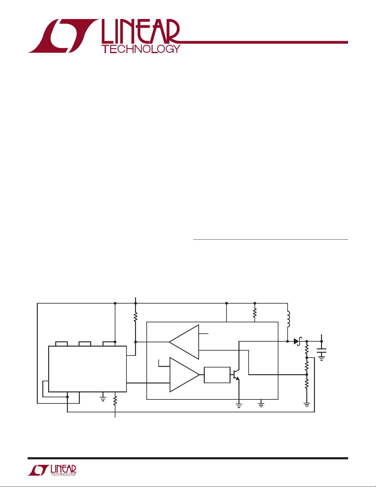
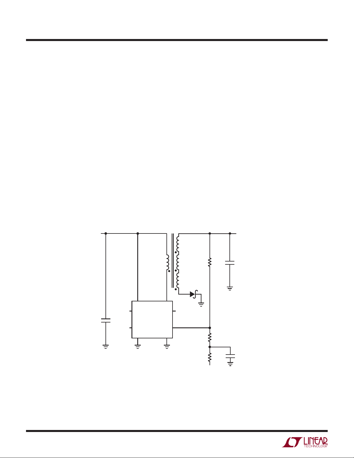
Clock Synchronized Switching Regulator
Gated oscillator type switching regulators permit high
efficiency over extended ranges of output current. These
regulators achieve this desirable characteristic by using
a gated oscillator architecture instead of a clocked pulse
width modulator. This eliminates the “housekeeping”
V
IN
2V TO 3.2V
(2 CELLS)
currents associated with the continuous operation of fixed
frequency designs. Gated oscillator regulators simply
self-clock at whatever frequency is required to maintain
the output voltage. Typically, loop oscillation frequency
ranges from a few hertz into the kilohertz region, depending upon the load.
In most cases this asynchronous, variable frequency operation does not create problems. Some systems, however, are
sensitive to this characteristic. Figure 1 slightly modifies
a gated oscillator type switching regulator by synchronizing its loop oscillation frequency to the systems clock. In
this fashion the oscillation frequency and its attendant
switching noise, albeit variable, become coherent with
system operation.
Note 1: “Study” is certainly a noble pursuit but we never fail to
emphasize use.
L, LT, LTC, LTM, Linear Technology and the Linear logo are registered trademarks of Linear
Technology Corporation. All other trademarks are the property of their respective owners.
SW2
47Ω
I
LIM
SW1
SET
GND
PRE1
CLR1
Q1
CLK1
74HC74
FLIP-FLOP
D1
PRE2CLR2Q1
V
CC
D2
Q2
CLK2
GND
47k
100kHz CLOCK
POWERED FROM
5V OUTPUT
100k
LT1107
A
OUT
V
1.2V
FB
REF
–
AUXILIARY
AMP
+
+
COMP
OSCILLATOR
–
L1 = COILTRONICS CTX-20-2
*= 1% METAL FILM RESISTOR
V
IN
V
REF
Figure 1. A Synchronizing Flip-Flop Forces Switching Regulator Noise to Be Coherent with the Clock
L1
22μH
1N5817
221k*
82.5k*
100k*
5V
OUT
+
100μF
AN61 F01
an61fa
AN61-1
Page 2

Application Note 61
Circuit operation is best understood by temporarily ignor-
®
ing the flip-flop and assuming the LT
and FB pins are connected. When the output voltage
A
OUT
decays the set pin drops below V
1107 regulator’s
, causing A
REF
OUT
to
fall. This causes the internal comparator to switch high,
biasing the oscillator and output transistor into conduction. L1 receives pulsed drive, and its flyback events are
deposited into the 100μF capacitor via the diode, restoring
output voltage. This overdrives the set pin, causing the IC
to switch off until another cycle is required. The frequency
of this oscillatory cycle is load dependent and variable. If,
as shown, a flip-flop is interposed in the A
-FB pin path,
OUT
synchronization to a system clock results. When the output
decays far enough (trace A, Figure 2) the A
pin (trace B)
OUT
goes low. At the next clock pulse (trace C) the flip-flop Q2
output (traceD) sets low, biasing the comparator-oscillator.
This turns on the power switch (V
pin is trace E), which
SW
pulses L1. L1 responds in flyback fashion, depositing its
energy into the output capacitor to maintain output voltage. This operation is similar to the previously described
case, except that the sequence is forced to synchronize
with the system clock by the flip-flops action. Although the
resulting loops oscillation frequency is variable it, and all
attendant switching noise, is synchronous and coherent
with the system clock.
A start-up sequence is required because this circuit’s
clock is powered from its output. The start-up circuitry
was developed by Sean Gold and Steve Pietkiewicz of
LTC. The flip-flop’s remaining section is connected as a
A = 50mV/DIV
AC-COUPLED
B = 5V/DIV
C = 5V/DIV
D = 5V/DIV
E = 5V/DIV
20μs/DIV
Figure 2. Waveforms for the Clock Synchronized
Switching Regulator. Regulator Only Switches (TraceE)
on Clock Transitions (Trace C), Resulting in Clock
Coherent Output Noise (Trace A)
AN61 F02
buffer. The CLR1-CLK1 line monitors output voltage via the
resistor string. When power is applied Q1 sets CLR2 low.
This permits the LT1107 to switch, raising output voltage.
When the output goes high enough Q1 sets CLR2 high
and normal loop operation commences.
The circuit shown is a step-up type, although any switching regulator configuration can utilize this synchronous
technique.
High Power 1.5V to 5V Converter
Some 1.5V powered systems (survival 2-way radios,
remote, transducer-fed data acquisition systems, etc.)
require much more power than stand-alone IC regulators
can provide. Figure 3’s design supplies a 5V output with
200mA capacity.
The circuit is essentially a flyback regulator. The LT1170
switching regulator’s low saturation losses and ease of
use permit high power operation and design simplicity.
Unfortunately this device has a 3V minimum supply requirement. Bootstrapping its supply pin from the 5V output is
possible, but requires some form of start-up mechanism.
1.5V
IN
+
47μF
L1
25μH
LT1170
1k
6.8μF
V
GND
SW
V
FB
IN
I
LIM
V
IN
V
C
+
L1 = PULSE ENGINEERING #PE-92100
* = 1% METAL FILM RESISTOR
Figure 3. 200mA Output 1.5V to 5V Converter. Lower
Voltage LT1073 Provides Bootstrap Start-Up for LT1170
High Power Switching Regulator
SW2
SW1
LT1073
1N5823
SENSE
GND
3.74k*
+
1k*
240Ω*
AN61 F03
5V
OUT
200mA MAX
470μF
AN61-2
an61fa
Page 3
Application Note 61
The 1.5V powered LT1073 switching regulator forms a
start-up loop. When power is applied the LT1073 runs,
causing its V
pin to periodically pull current through L1.
SW
L1 responds with high voltage flyback events. These events
are rectified and stored in the 470μF capacitor, producing
the circuits DC output. The output divider string is set up
so the LT1073 turns off when circuit output crosses about
4.5V. Under these conditions the LT1073 obviously can no
longer drive L1, but the LT1170 can. When the start-up
circuit goes off, the LT1170 V
pin has adequate supply
IN
voltage and can operate. There is some overlap between
start-up loop turn-off and LT1170 turn-on, but it has no
detrimental effect.
The start-up loop must function over a wide range of
loads and battery voltages. Start-up currents approach
1A, necessitating attention to the LT1073’s saturation and
drive characteristics. The worst case is a nearly depleted
battery and heavy output loading.
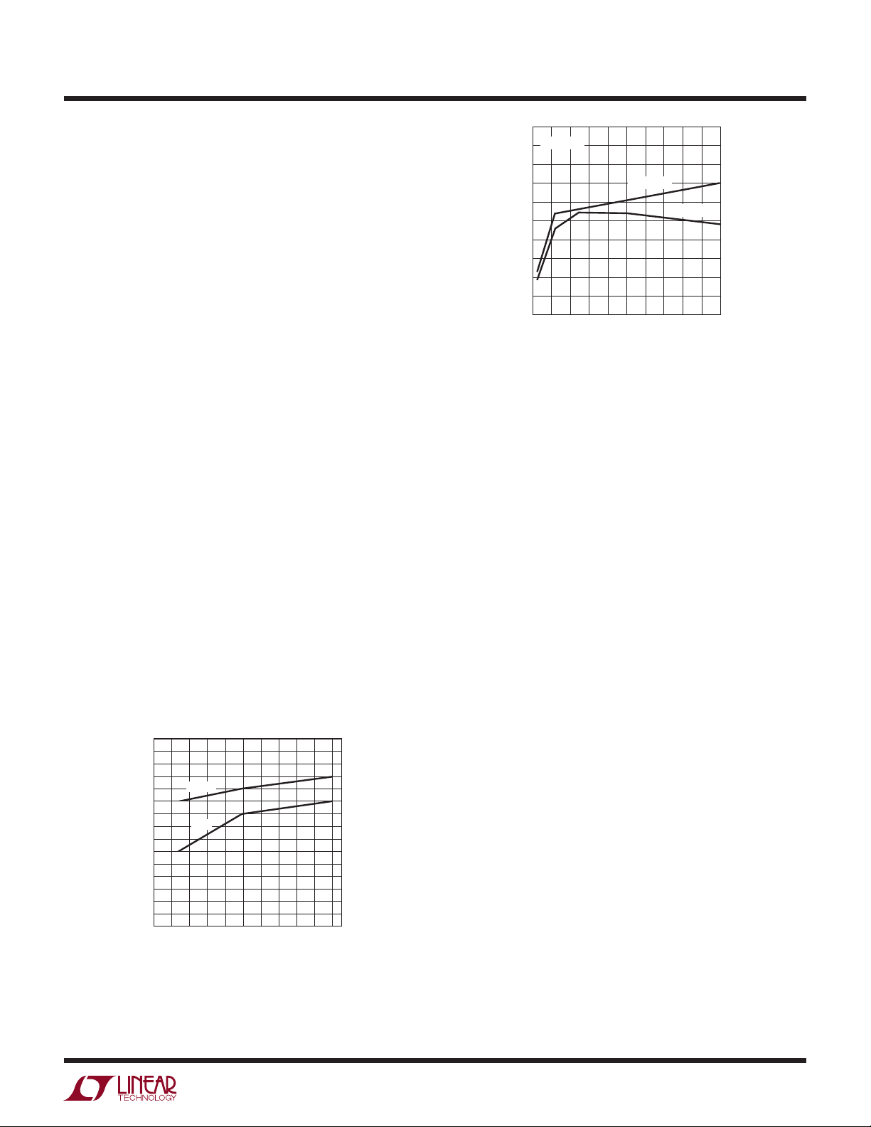
Figure 4 plots input-output characteristics for the circuit.
Note that the circuit will start into all loads with V
BAT
=
1.2V. Start-up is possible down to 1.0V at reduced loads.
Once the circuit has started, the plot shows it will drive full
200mA loads down to V
sible down to V
= 0.6V (a very dead battery)! Figure5
BAT
= 1.0V. Reduced drive is pos-
BAT
graphs efficiency at two supply voltages over a range of
output currents. Performance is attractive, although at
lower currents circuit quiescent power degrades efficiency.
Fixed junction saturation losses are responsible for lower
overall efficiency at the lower supply voltage.
1.5
= 5V
1.4
OUT
1.3
1.2
1.1
1.0
0.9
0.8
0.7
0.6
0.5
0.4
0.3
0.2
0.1
0
MINIMUM INPUT VOLTAGE TO MAINTAIN V
START
RUN
120 140
100
0
60 80
20
40
OUTPUT CURRENT (mA)
160 180
200
AN61 F04
100
V
= 5V
OUT
90
80
70
60
50
40
EFFICIENCY (%)
30
20
10
0
0 20 40 60 80 100 120
OUTPUT CURRENT (mA)
VIN = 1.5V
VIN = 1.2V
140 160 180 200
AN61 F05
Figure 5. Efficiency vs Operating Point for the 1.5V to
5V Converter. Efficiency Suffers at Low Power Because
of Relatively High Quiescent Currents
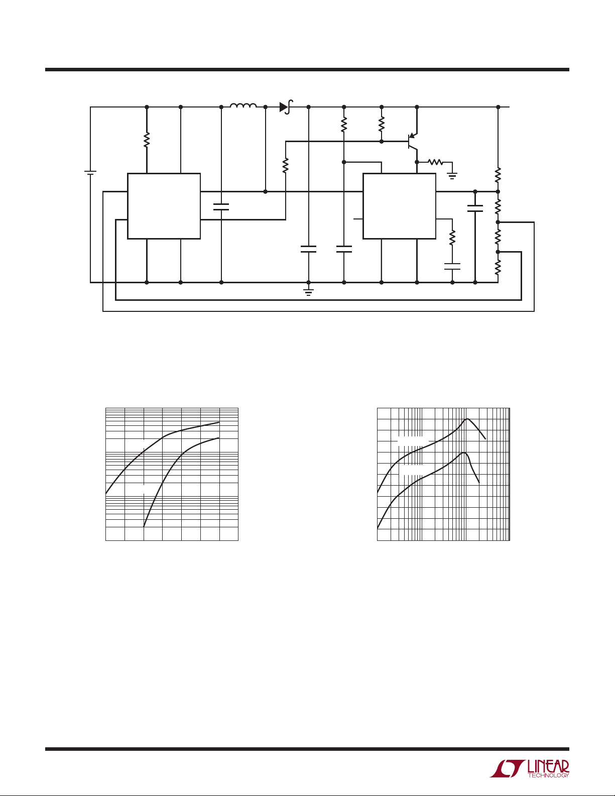
Low Power 1.5V to 5V Converter
Figure 6, essentially the same approach as the preceding circuit, was developed by Steve Pietkiewicz of LTC.
It is limited to about 150mA output with commensurate
restrictions on start-up current. It’s advantage, good efficiency at relatively low output currents, derives from its
low quiescent power consumption.
The LT1073 provides circuit start-up. When output voltage,
sensed by the LT1073’s “set” input via the resistor divider,
rises high enough Q1 turns on, enabling the LT1302. This
device sees adequate operating voltage and responds by
driving the output to 5V, satisfying its feedback node. The
5V output also causes enough overdrive at the LT1073
feedback pin to shut the device down.
Figure 7 shows maximum permissible load currents for
start-up and running conditions. Performance is quite
good, although the circuit clearly cannot compete with the
previous design. The fundamental difference between the
two circuits is the LT1170’s (Figure 3) much larger power
switch, which is responsible for the higher available power.
Figure 8, however, reveals another difference. The curves
show that Figure 6 is significantly more efficient than the
LT1170 based approach at output currents below 100mA.
This highly desirable characteristic is due to the LT1302’s
much lower quiescent operating currents.
Figure 4. Input-Output Data for the 1.5V to 5V
Converter Shows Extremely Wide Start-Up and
Running Range into Full Load
an61fa
AN61-3
Page 4
Application Note 61
220Ω
1.5V
CELL
C1 = AVX TPSD476M016R0150
C2 = AVX TPSE227M010R0100
SET
FB
I
LIM
GND
LT1073
V
SW2
IN
SW1
A
L1
3.3μH
+
C1
47μF
O
L1 = COILCRAFT DO3316-332
D1 = MOTOROLA MBR3130LT3
D1
100k
220μF
10Ω
NC
+
C2
0.1μF
Figure 6. Single-Cell to 5V Converter Delivers 150mA
with Good Efficiency at Lower Currents
SW
I
LIM
V
IN
PGND
100k
LT1302
SHDN
GND
Q1
2N3906
100k
FB
V
C
0.01μF
100pF
20k
R1
301k
1%
56.2k
1%
4.99k
1%
36.5k
1%
5V
OUT
AN61 F06
1000
100
10
MAXIMUM LOAD CURRENT (mA )
1
RUN
START
0.6
1.0 1.2 1.4 1.81.6
0.8 2.0
INPUT VOLTAGE (V)
AN61 F07
Figure 7. Maximum Permissible Loads for Start-Up
and Running Conditions. Allowable Load Current
During Start-Up Is Substantially Less Than Maximum
Running Current.
72
70
68
66
64
62
60
58
EFFICIENCY (%)
56
54
52
50
48
VIN = 1.5V
VIN = 1.2V
1
10 100 1000
LOAD CURRENT (mA)
AN61 F08
Figure 8. Efficiency Plot for Figure 6. Performance
Is Better Than the Previous Circuit at Lower
Currents, Although Poorer at High Power
AN61-4
an61fa
Page 5
Application Note 61
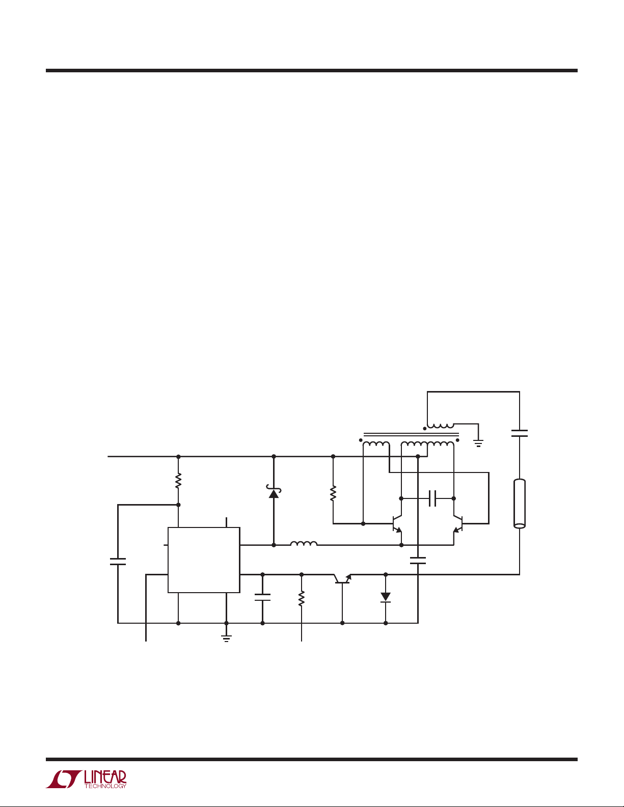
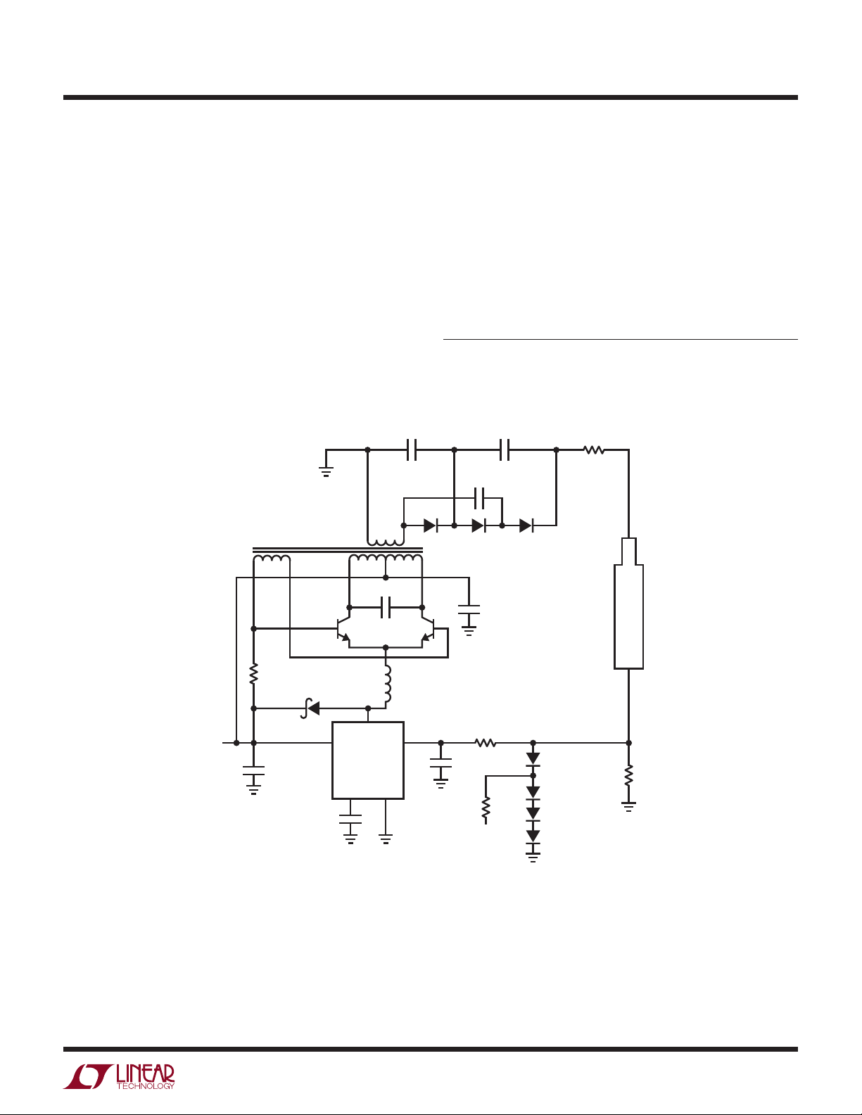
Low Power, Low Voltage Cold Cathode Fluorescent
Lamp Power Supply
Most Cold Cathode Fluorescent Lamp (CCFL) circuits
require an input supply of 5V to 30V and are optimized
for bulb currents of 5mA or more. This precludes lower
power operation from 2- or 3-cell batteries often used in
palmtop computers and portable apparatus. A CCFL power
supply that operates from 2V to 6V is detailed in Figure 9.
This circuit, contributed by Steve Pietkiewicz of LTC, can
drive a small CCFL over a 100μA to 2mA range.
The circuit uses an LT1301 micropower DC/DC converter IC
in conjunction with a current driven Royer class converter
comprised of T1, Q1 and Q2. When power and intensity
adjust voltage are applied the LT1301’s I
pin is driven
LIM
slightly positive, causing maximum switching current
through the IC’s internal switch pin (SW). Current flows
from T1’s center tap, through the transistors, into L1. L1’s
current is deposited in switched fashion to ground by the
regulator’s action.
The Royer converter oscillates at a frequency primarily
set by T1’s characteristics (including its load) and the
0.068μF capacitor. LT1301 driven L1 sets the magnitude of
the Q1-Q2 tail current, hence T1’s drive level. The 1N5817
diode maintains L1’s current flow when the LT1301’s
switch is off. The 0.068μF capacitor combines with T1’s
characteristics to produce sine wave voltage drive at the
Q1 and Q2 collectors. T1 furnishes voltage step-up and
about 1400Vp-p appears at its secondary. Alternating current flows through the 22pF capacitor into the lamp. On
positive half-cycles the lamp’s current is steered to ground
via D1. On negative half-cycles the lamp’s current flows
through Q3’s collector and is filtered by C1. The LT1301’s
pin acts as a 0V summing point with about 25μA
I
LIM
bias current flowing out of the pin into C1. The LT1301
regulates L1’s current to equalize Q3’s average collector
current, representing 1/2 the lamp current, and R1’s current, represented by V
to DC. When V
is set to zero, the I
A
/R1. C1 smooths all current flow
A
pin’s bias current
LIM
forces about 100μA bulb current.
97
V
2V TO 6V
IN
NC
0.1μF
SHUTDOWN
T1 = COILTRONICS CTX110654-1
L1 = COILCRAFT D03316-473
0.68μF = WIMA MKP-20
V
IN
SENSE
SHDN
GND
1Ω
LT1301
SELECT
SW
I
LIM
PGND
1N5817
L1
47μH
+
C1
1μF
INTENSITY ADJUST
100μA TO 2mA BULB CURRENT
R1
7.5K
1%
V
0V TO 5VDC
120Ω
Q3
2N3904
A
IN
15TI4
Q1
ZTX849
D1
1N4148
32
0.68μF
+
10μF
Q2
ZTX849
AN61 F09
Figure 9. Low Power Cold Cathode Fluorescent Lamp Supply Is Optimized for Low Voltage Inputs and Small Lamps
22pF
3kV
CCFL
an61fa
AN61-5
Page 6
Application Note 61
Circuit efficiency ranges from 80% to 88% at full load, depending on line voltage. Current mode operation combined
with the Royer’s consistent waveshape vs input results
in excellent line rejection. The circuit has none of the line
rejection problems attributable to the hysteretic voltage
control loops typically found in low voltage micropower
DC/DC converters. This is an especially desirable characteristic for CCFL control, where lamp intensity must remain
constant with shifts in line voltage. Interaction between
the Royer converter, the lamp and the regulation loop is
far more complex than might be supposed, and subject
to a variety of considerations. For detailed discussion see
Reference 3.
Low Voltage Powered LCD Contrast Supply
Figure 10, a companion to the CCFL power supply previously described, is a contrast supply for LCD panels. It
was designed by Steve Pietkiewicz of LTC. The circuit is
noteworthy because it operates from a 1.8V to 6V input,
significantly lower than most designs. In operation the
LT1300/LT1301 switching regulator drives T1 in flyback
fashion, causing negative biased step-up at T1’s secondary. D1 provides rectification, and C1 smooths the
output to DC. The resistively divided output is compared
to a command input, which may be DC or PWM, by the
IC’s “I
the I
” pin. The IC, forcing the loop to maintain 0V at
LIM
pin, regulates circuit output in proportion to the
LIM
command input.
Efficiency ranges from 77% to 83% as supply voltage
varies from 1.8V to 3V. At the same supply limits, available
output current increases from 12mA to 25mA.
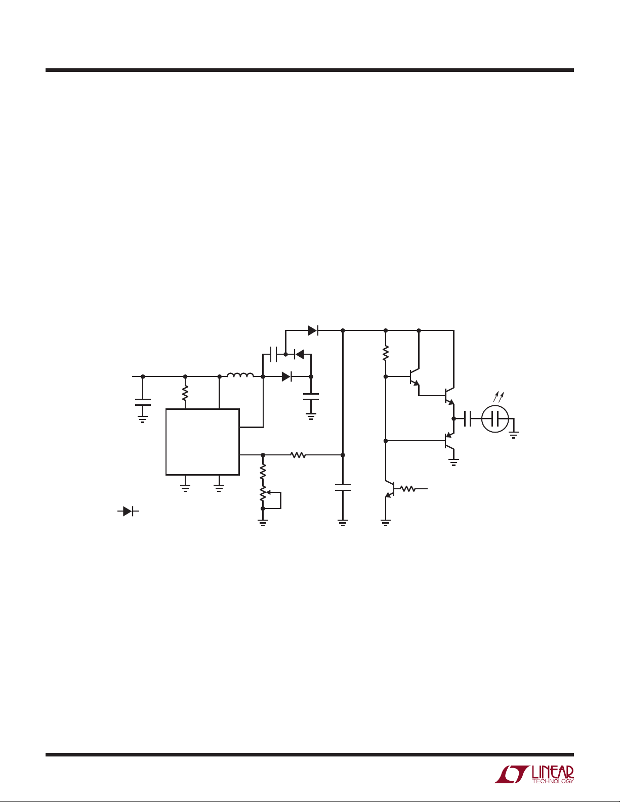
HeNe Laser Power Supply
Helium-Neon lasers, used for a variety of tasks, are difficult loads for a power supply. They typically need almost
10kV to start conduction, although they require only about
1500V to maintain conduction at their specified operating
currents. Powering a laser usually involves some form
of start-up circuitry to generate the initial breakdown
voltage and a separate supply for sustaining conduction.
Figure11’s circuit considerably simplifies driving the laser.
V
1.8V TO 6V
IN
+
100μF
T1 = DALE LPE-5047-AO45
NC
NC
V
IN
SENSE
SELECT
PGND
LT1300
OR
LT1301
1
10
SW
SHDN
I
LIM
GND
T1
SHUTDOWN
4
7
3
8
2
9
1N5819
D1
COMMAND INPUT
PWM OR DC
0% TO 100%
OR 0V TO 5V
150k
12k
12k
CONTRAST OUTPUT
V
OUT
C1
22μF
+
35V
+
2.2μF
–4V TO –29V
AN61 F10
AN61-6
Figure 10. Liquid Crystal Display Contrast Supply Operates from 1.8V to 6V with –4V to –29V Output Range
an61fa
Page 7
Application Note 61
The start-up and sustaining functions have been combined
into a single, closed-loop current source with over 10kV
of compliance. The circuit is recognizable as a reworked
2
CCFL power supply with a voltage tripled DC output.
When power is applied, the laser does not conduct and
the voltage across the 190Ω resistor is zero. The LT1170
switching regulator FB pin sees no feedback voltage, and
its switch pin (V
) provides full duty cycle pulse width
SW
modulation to L2. Current flows from L1’s center tap
through Q1 and Q2 into L2 and the LT1170. This current
flow causes Q1 and Q2 to switch, alternately driving L1.
The 0.47μF capacitor resonates with L1, providing boosted
sine wave drive. L1 provides substantial step-up, causing
0.01μF
5kV
about 3500V to appear at its secondary. The capacitors and
diodes associated with L1’s secondary form a voltage tripler,
producing over 10kV across the laser. The laser breaks
down and current begins to flow through it. The 47k resistor
limits current and isolates the laser’s load characteristic.
The current flow causes a voltage to appear across the
190Ω resistor. A filtered version of this voltage appears
at the LT1170 FB pin, closing a control loop. The LT1170
adjusts pulse width drive to L2 to maintain the FB pin at
1.23V, regardless of changes in operating conditions. In
this fashion, the laser sees constant current drive, in this
Note 2: See References 2 and 3 and this text’s Figure 9.
1800pF
10kV
1800pF
10kV
47k
5W
V
IN
9V TO 35V
HV DIODES =
0.47μF =
Q1, Q2 =
LASER =
L1
5
+
SEMTECH-FM-50
WIMA 3w 0.15μF TYPE MKP-20
ZETEX ZTX849
L1 =
COILTRONICS CTX02-11128-2
L2 =
PULSE ENGINEERING PE-92105
HUGHES 3121H-P
4
150Ω
MUR405
2.2μF
10μF
V
1
+
IN
V
11
Q1
V
LT1170
C
SW
0.47μF
GND
2
L2
145μH
FB
8
Q2
3
HV DIODES
+
2.2μF
10k
0.1μF
V
IN
10k
1N4002
(ALL)
LASER
190Ω
1%
AN61 F11
Figure 11. LASER Power Supply Is Essentially A 10,000V Compliance Current Source
an61fa
AN61-7
Page 8
Application Note 61
case 6.5mA. Other currents are obtainable by varying the
190Ω value. The 1N4002 diode string clamps excessive
voltages when laser conduction first begins, protecting
the LT1170. The 10μF capacitor at the V
pin frequency
C
compensates the loop and the MUR405 maintains L1’s
current flow when the LT1170 V
pin is not conducting.
SW
The circuit will start and run the laser over a 9V to 35V
input range with an electrical efficiency of about 80%.
Compact Electroluminescent Panel Power Supply
Electroluminescent (EL) panel LCD backlighting presents an
attractive alternative to fluorescent tube (CCFL) backlighting
in some portable systems. EL panels are thin, lightweight,
lower power, require no diffuser and work at lower voltage
than CCFLs. Unfortunately, most EL DC/AC inverters use a
0.1μF
100V
L1
V
SW2
100μH
+
IN
SW1
2.26M
FB
30.1k
R1
25k
V
2V TO 12V
33pF
IN
+
= MOTOROLA MURS120T3
L1 = COILCRAFT DO3316-104
47Ω
I
LIM
U1
LT1108CS8
GND
large transformer to generate the 400Hz 95V square wave
required to drive the panel. Figure 12’s circuit, developed
by Steve Pietkiewicz of LTC, eliminates the transformer
by employing an LT1108 micropower DC/DC converter
IC. The device generates a 95VDC potential via L1 and the
diode-capacitor doubler network. The transistors switch
the EL panel between 95V and ground. C1 blocks DC and
R1 allows intensity adjustment. The 400Hz square wave
drive signal can be supplied by the microprocessor or a
simple multivibrator. When compared to conventional EL
panel supplies, this circuit is noteworthy because it can
be built in a square inch with a 0.5 inch height restriction.
Additionally, all components are surface mount types, and
the usual large and heavy 400Hz transformer is eliminated.
95V
1M
MMBTA42
0.1μF
100V
0.47μF
200V
MMBTA42
10k
MMBTA42
400Hz DRIVE
SQUARE WAVE
C1
1μF
100V
MMBTA92
EL
PANEL
AN61 F12
AN61-8
Figure 12. Switch Mode EL Panel Driver Eliminates Large 400Hz Transformer
an61fa
Page 9
Application Note 61
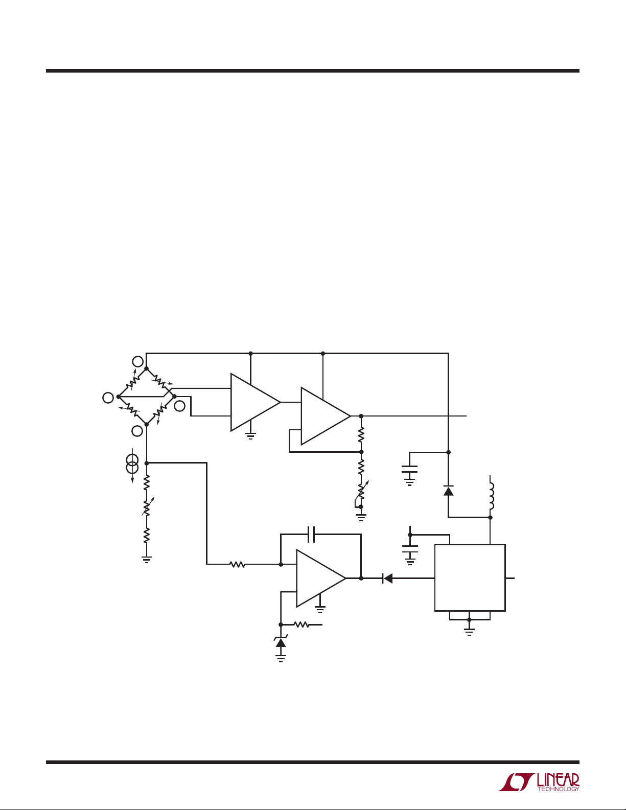
3.3V Powered Barometric Pressure Signal Conditioner
The move to 3.3V digital supply voltage creates problems
for analog signal conditioning. In particular, transducer
based circuits often require higher voltage for proper
transducer excitation. DC/DC converters in standard
configurations can address this issue but increase power
consumption. Figure 13’s circuit shows a way to provide
proper transducer excitation for a barometric pressure
sensor while minimizing power requirements.
The 6kΩ transducer T1 requires precisely 1.5mA of excitation, necessitating a relatively high voltage drive. A1
senses T1’s current by monitoring the voltage drop across
the resistor string in T1’s return path.
A = 10
–
1/2 LT1078
+
LT1034
1.2V
A1
≈10V DURING OPERATIONT1
3.3V
+
A3
1/2 LT1078
–
0.05μF
1μF
1N4148
10k
3.3V
PRESSURE
TRANSDUCER
5
10
6
BRIDGE
CURRENT
TRIM
BRIDGE
CURRENT
MONITOR
(0.1500V)
* = 1% FILM RESISTOR
** = 0.1% FILM RESISTOR
L1 = TOKO 262-LYF-0095K
T1 = NOVASENSOR (FREMONT, CA)
NPH-8-100AH
4
700Ω*
50Ω
100Ω**
100k
1μF
–
A2
LT1101
+
A1’s output biases the LT1172 switching regulator’s operating point, producing a stepped up DC voltage which
appears as T1’s drive and A2’s supply voltage. T1’s return
current out of pin 6 closes a loop back at A1 which is
slaved to the 1.2V reference. This arrangement provides
the required high voltage drive (≈10V) while minimizing
power consumption. This is so because the switching
regulator produces only enough voltage to satisfy T1’s
current requirements. Instrumentation amplifier A2 and A3
®
provide gain and LTC
1287 A/D converter gives a 12-bit
digital output. A2 is bootstrapped off the transducer supply,
enabling it to accept T1’s common-mode voltage. Circuit
current consumption is about 14mA. If the shutdown pin
is driven high the switching regulator turns off, reducing
2N3904
10k*
1M
CALIB
2.2μF
100k
+
3.3V
+
22μF
V
V
C
SHUTDOWN
1N752
5.6V
MUR110
IN
LT1172
TO PROCESSOR
CS
+IN
–IN
3.3V
L1
150μH
V
SW
FB
GNDE2E1
CLK D
LTC1287
GND
NC
OUT
V
REF
V
CC
1N4148
AN61 F13
3.3V
Figure 13. 3.3V Powered, Digital Output, Barometric Pressure Signal Conditioner
an61fa
AN61-9
Page 10
Application Note 61
total power consumption to about 1mA. In shutdown the
3.3V powered A/D’s output data remains valid. In practice,
the circuit provides a 12-bit representation of ambient
barometric pressure after calibration. To calibrate, adjust
the “bridge current trim” for exactly 0.1500V at the indicated
point. This sets T1’s current to the manufacturers specified point. Next, adjust A3’s trim so that the digital output
corresponds to the known ambient barometric pressure.
If a pressure standard is not available the transducer is
supplied with individual calibration data, permitting circuit
calibration.
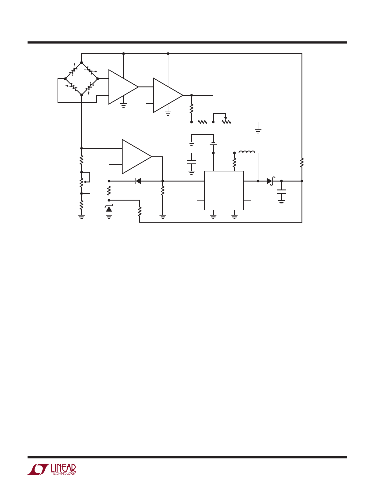
Some applications may require operation over a wider
supply range and/or a calibrated analog output. Figure14’s
circuit is quite similar, except that the A/D converter is
eliminated and a 2.7V to 7V supply is acceptable. The
calibration procedure is identical, except that A3’s analog
output is monitored.
5
T1
10
6
4
–
LT1101
+
A = 10
A2
+
1/2 LT1078
–
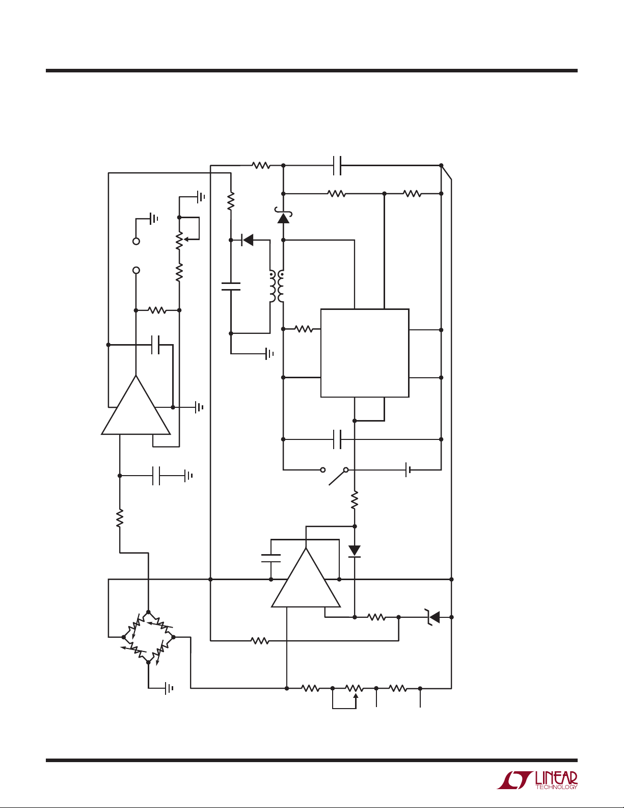
Single Cell Barometers
It is possible to power these circuits from a single cell without sacrificing performance. Figure 15, a direct extension
of the above approaches, simply substitutes a switching
regulator that will run from a single 1.5V battery. In other
respects loop action is nearly identical.
Figure 16, also a 1.5V powered design, is related but
eliminates the instrumentation amplifier. As before, the
6kΩ transducer T1 requires precisely 1.5mA of excitation,
necessitating a relatively high voltage drive. A1’s positive
input senses T1’s current by monitoring the voltage drop
across the resistor string in T1’s return path. A1’s negative
input is fixed by the 1.2V LT1004 reference. A1’s output
biases the 1.5V powered LT1110 switching regulator. The
LT1110’s switching produces two outputs from L1. Pin4’s
rectified and filtered output powers A1 and T1. A1’s output,
A3
20k*
OUTPUT
0V TO 3.100V =
0 TO 31.00" Hg.
2.2μF
1N4148
+
3.3V
+
22μF
3.3V
MUR110
V
IN
V
C
V
LT1172
GNDE2E1
1.500mA
700Ω*
BRIDGE
CURRENT
* = 1% FILM RESISTOR
L1 = TOKO 262-LYF-0095K
T1 = NOVASENSOR NPH-8-100AH
50Ω
TRIM
100Ω
0.1%
100k
–
1/2 LT1078
+
10k
LT1034
1.2V
1μF
10k*
OUTPUT
A1
3.3V
TRIM
1k
Figure 14. Single Supply Barometric Pressure Signal Conditioner Operates Over a 2.7V to 7V Range
SW
L1
150μH
FB
NC
AN61 F13
an61fa
AN61-10
Page 11
Application Note 61
T1
5
10
50Ω
TRIM FOR
150mV AT
POINT “A”
* = 1% FILM RESISTOR
L1 = COILTRONICS CTX50-1
T1 = NOVASENSOR NPH-8-100AH
4
6
700Ω
1%
A
100Ω
0.1%
–
A2
LT1101
+
100k
LT1004-1.2
A =10
+
A1
1/2 LT1078
–
100k
+
–
A3
LT1078
10k
OUTPUT
0 TO 3.100V=
0 TO 31.00"Hg
200k*
100k*
10k
CAL
1.5V
AA CELL
+
1μF
V
IN
FB
LT1110
SET
150
I
L
SW1
AONC NC
SW2GND
L1
50μH
1N5818
100Ω
+
150μF
AN61 F15
Figure 15. 1.5V Powered Barometric Pressure Signal Conditioner Uses
Instrumentation Amplifier and Voltage Boosted Current Loop
in turn, closes a feedback loop at the regulator. This loop
generates whatever voltage step-up is required to force
precisely 1.5mA through T1. This arrangement provides
the required high voltage drive while minimizing power
consumption. This occurs because the switching regulator produces only enough voltage to satisfy T1’s current
requirements.
L1 pins 1 and 2 source a boosted, fully floating voltage,
which is rectified and filtered. This potential powers A2.
Because A2 floats with respect to T1, it can look differentially across T1’s outputs, pins 10 and 4. In practice,
pin10 becomes “ground” and A2 measures pin 4’s output
with respect to this point. A2’s gain-scaled output is the
circuit’s output, conveniently scaled at 3.000V = 30.00"Hg.
A2’s floating drive eliminates the requirement for an
instrumentation amplifier, saving cost, power, space and
error contribution.
To calibrate the circuit, adjust R1 for 150mV across the
100Ω resistor in T1’s return path. This sets T1’s current
to the manufacturer’s specified calibration point. Next,
adjust R2 at a scale factor of 3.000V = 30.00"Hg. If R2
cannot capture the calibration, reselect the 200k resistor
in series with it. If a pressure standard is not available,
the transducer is supplied with individual calibration data,
permitting circuit calibration.
This circuit, compared to a high-order pressure standard,
maintained 0.01"Hg accuracy over months with widely
varying ambient pressure shifts. Changes in pressure,
particularly rapid ones, correlated quite nicely to changing
weather conditions. Additionally, because 0.01"Hg corresponds to about 10 feet of altitude at sea level, driving over
hills and freeway overpasses becomes quite interesting.
an61fa
AN61-11
Page 12
Application Note 61
"Hg.
0V TO 3.100V =
0 TO 31.00
OUTPUT
200k*
0.1μF
A2
LT1077
+
–
R2
10k
1%
1k
1%
100Ω
+
1N4148
100μF
100Ω
1N5818
1
2
390μF
16V
NICHICON
PL
+
430k
4
L1
3
L
I
150Ω
21
IN
V
83
1μF
SW1
FB
LT1110
AN61 F16
39k
7
SET
SW2
54
GND
AO
6
L1 = COILTRONICS CTX50-1
68k
5
†
T1
NOVASENSOR
NPH-8-100AH
4
10
1μF
NON-POLAR
+
= LUCAS NOVASENSOR
FREMONT, CA (510) 490-9100
†
100k
100Ω
0.1%
AA CELL
A2
LT1004-1.2
Figure 16. 1.5V Powered Barometric Pressure Signal Conditioner Floats Bridge Drive to
Eliminate Instrumentation Amplifier. Voltage Boosted Current Loop Drives Transducer
* = NOMINAL VALUE. EACH SENSOR REQUIRES SELECTION
** = TRIM FOR 150mV ACROSS A1-A2
100k
R1**
1N4148
50Ω
A1
0.1μF
A1
LT1077
+
6
100k
698Ω
–
1%
AN61-12
an61fa
Page 13

Application Note 61
Until recently, this type of accuracy and stability has only
been attainable with bonded strain gauge and capacitivelybased transducers, which are quite expensive. As such,
semiconductor pressure transducer manufacturers whose
products perform at the levels reported are to be applauded.
Although high quality semiconductor transducers are still
not comparable to more mature technologies, their cost
is low and they are vastly improved over earlier devices.
The circuit pulls 14mA from the battery, allowing about
250 hours operation from one D cell.
Quartz Crystal-Based Thermometer
Although quartz crystals have been utilized as temperature sensors (see Reference 5), there has been almost no
widespread adaptation of this technology. This is primarily
due to the lack of standard product quartz-based temperature sensors. The advantages of quartz-based sensors
include simple signal conditioning, good stability and a
direct, noise immune digital output almost ideally suited
to remote sensing.
Figure 17 utilizes an economical, commercially available
(see Reference 6) quartz-based temperature sensor in a
thermometer scheme suited to remote data collection.
The LTC485 RS485 transceiver is set up in the transmit
6
7
2
5V
8
LTC485
3
5
1
4
NC
0°C TO 100°C
= 261.900kHz
– 262.800kHz
OUT
"/t'
10M
6
4
LTC485
1
NC
+33.5ppm/°C
10pF
Figure 17. Quartz Crystal Based Circuit Provides
Temperature-to-Frequency Conversion. RS485
Transceivers Allow Remote Sensing
7
3
2
8
5
5V
Y1
1000 FEET
TWISTED-PAIR
100k
15pF
100Ω
Y1 = MICRO CRYSTAL (SWISS)
MT1/33.5ppm/°C
0°C = 261.900kHz
100°C = 262.800kHz
mode. The crystal and discrete components combine
with the IC’s inverting gain to form a Pierce type oscillator. The LTC485’s differential line driving outputs provide
frequency coded temperature data to a 1000-foot cable
run. A second RS485 transceiver differentially receives
the data and presents a single-ended output. Accuracy
depends on the grade of quartz sensor specified, with 1°C
over 0°C to 100°C achievable.
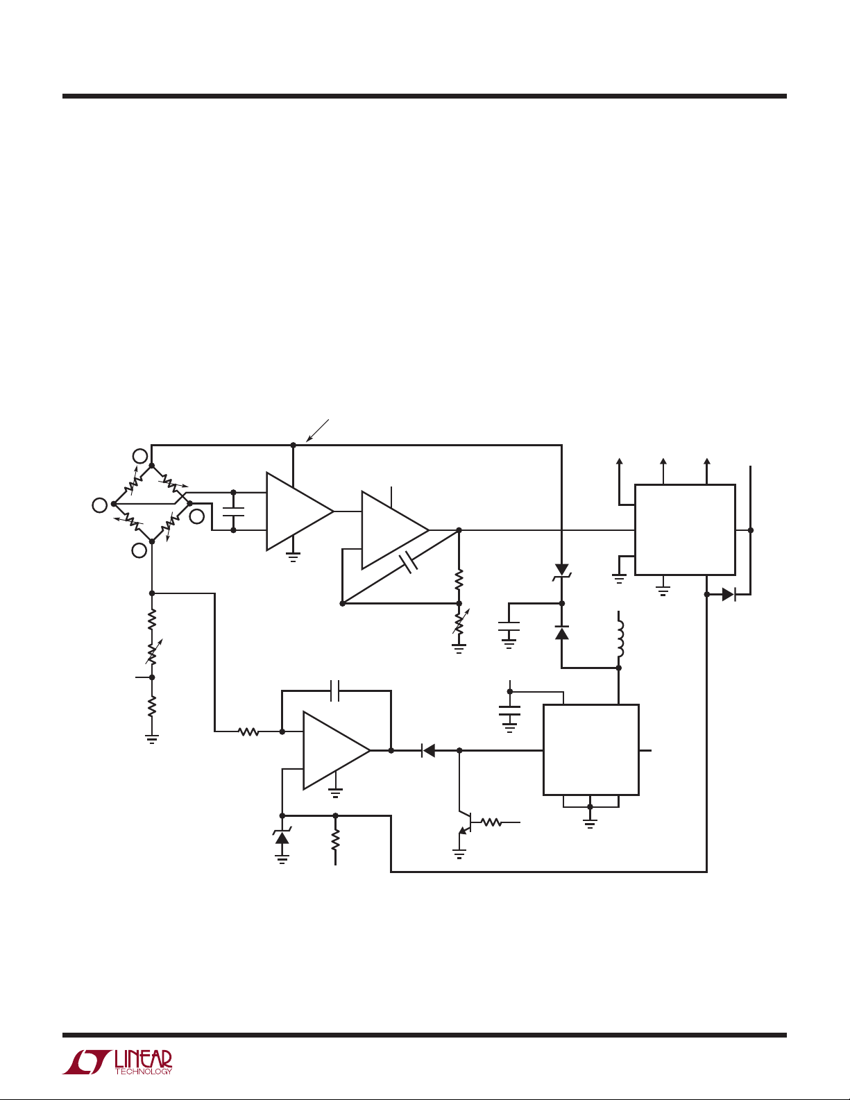
Ultra-Low Noise and Low Drift Chopped-FET Amplifier
Figure 18’s circuit combines the extremely low drift of
a chopper-stabilized amplifier with a pair of low noise
FETs. The result is an amplifier with 0.05μV/°C drift, offset
within 5μV, 100pA bias current and 50nV noise in a 0.1Hz
to 10Hz bandwidth. The noise performance is especially
noteworthy; it is almost 35 times better than monolithic
chopper-stabilized amplifiers and equals the best bipolar
types.
FETs Q1 and Q2 differentially feed A2 to form a simple
low noise op amp. Feedback, provided by R1 and R2,
sets closed-loop gain (in this case 10,000) in the usual
fashion. Although Q1 and Q2 have extraordinarily low noise
characteristics, their offset and drift are uncontrolled. A1,
a chopper-stabilized amplifier, corrects these deficiencies.
It does this by measuring the difference between the
amplifier’s inputs and adjusting Q1’s channel current via
Q3 to minimize the difference. Q1’s skewed drain values
ensure that A1 will be able to capture the offset. A1 and
Q3 supply whatever current is required into Q1’s channel to force offset within 5μV. Additionally, A1’s low bias
current does not appreciably add to the overall 100pA
amplifier bias current. As shown, the amplifier is set up
for a noninverting gain of 10,000 although other gains
and inverting operation are possible. Figure 19 is a plot
of the measured noise performance.
The FETs’ V
they must be selected for 10% V
can vary over a 4:1 range. Because of this,
GS
matching. This match-
GS
ing allows A1 to capture the offset without introducing
any significant noise.
an61fa
AN61-13
Page 14

Application Note 61
15V
0.02μF
+
A1
LTC1150
–
–15V
100k100k
+ INPUT
* = 1% FILM RESISTOR
Q1, Q2 = 2SK147 TOSHIBA
0.02μF
10k
Q3
2N2907
–15V
1k*
450Ω*
Q1
–15V
200Ω*
15V
Q2
750Ω*
900Ω*
COMPENSATION
– INPUT
–
A2
LT1097
+
OPTIONAL
OVER
OUTPUT
5
R1
100k
R2
Ω10
Figure 18. Chopper-Stabilized FET Pair Combines Low Bias, Offset and Drift with 45nV Noise
AN61 F18
100
NANOVOLTS
AN61 F19
10 SECONDS
Figure 19. Figure 18’s 45nV Noise Performance in a 0.1Hz to 10Hz Bandwidth.
A1’s Low Offset and Drift Are Retained, But Noise Is Almost 35 Times Better
an61fa
AN61-14
Page 15

Application Note 61
Figure 20 shows the response (trace B) to a 1mV input
step (trace A). The output is clean, with no overshoots or
uncontrolled components. If A2 is replaced with a faster
device (e.g., LT1055) speed increases by an order of
magnitude with similar damping. A2’s optional overcompensation can be used (capacitor to ground) to optimize
response for low closed-loop gains.
A = 500μV/DIV
B = 5V/DIV
100μs/DIV
Figure 20. Step Response for the Low Noise × 10,000
Amplifier. A 10× Speed Increase Is Obtainable by
Replacing A2 with a Faster Device
AN61 F20
High Speed Adaptive Trigger Circuit
Line receivers often require an adaptive trigger to compensate for variations in signal amplitude and DC offsets. The
circuit in Figure 21 triggers on 2mV to 100mV signals from
100Hz to 10MHz while operating from a single 5V rail. A1,
operating at a gain of 20, provides wideband AC gain. The
output of this stage biases a 2-way peak detector (Q1-Q4).
The maximum peak is stored in Q2’s emitter capacitor,
while the minimum excursion is retained in Q4’s emitter
capacitor. The DC value of A1’s output signal’s midpoint
appears at the junction of the 500pF capacitor and the
10MΩ units. This point always sits midway between the
signal’s excursions, regardless of absolute amplitude. This
signal-adaptive voltage is buffered by A2 to set the trigger
voltage at the LT1116’s positive input. The LT1116’s negative input is biased directly from A1’s output. The LT1116’s
output, the circuit’s output, is unaffected by 50:1 signal
amplitude variations. Bandwidth limiting in A1 does not
affect triggering because the adaptive trigger threshold
varies ratiometrically to maintain circuit output.
Split supply versions of this circuit can achieve bandwidths to 50MHz with wider input operating range (See
Reference 7).
5V
3k
Q1
5V
+
A1
LT1192
–
50Ω
C1
100μF
1k
Q3
C2
0.1μF
NPN = 2N3904
PNP = 2N3906
2k
INPUT
750Ω
0.01μF
+
5V
10μF
+
0.005μF
0.005μF
3k
500Ω
Q2
500pF
10M
5V
+
10M
A2
LT1006
–
Q4
+
LT1116
–
5V
Q
Q
TRIGGER
OUT
AN61 F21
1N4148
1N4148
500Ω
0.1μF
Figure 21. Fast Single Supply Adaptive Trigger. Output Comparator’s Trip Level Varies Ratiometrically
with Input Amplitude, Maintaining Data Integrity Over 50:1 Input Amplitude Range
an61fa
AN61-15
Page 16

Application Note 61
Wideband, Thermally-Based RMS/DC Converter
Applications such as wideband RMS voltmeters, RF leveling
loops, wideband AGC, high crest factor measurements,
SCR power monitoring and high frequency noise measurements require wideband, true RMS/DC conversion.
The thermal conversion method achieves vastly higher
bandwidth than any other approach. Thermal RMS/DC
converters are direct acting, thermoelectronic analog
computers. The thermal technique is explicit, relying on
“first principles,” e.g,. a waveforms RMS value is defined
as its heating value in a load.
Figure 22 is a wideband, thermally-based RMS/DC con-
3
verter.
It provides a true RMS/DC conversion from DC
to 10MHz with less than 1% error, regardless of input
signal waveshape. It also features high input impedance
and overload protection.
The circuit consists of three blocks; a wideband FET input
amplifier, the RMS/DC converter and overload protection.
The amplifier provides high input impedance, gain and
drives the RMS/DC converters input heater. Input resistance
is defined by the 1M resistor with input capacitance about
3pF. Q1 and Q2 constitute a simple, high speed FET input
buffer. Q1 functions as a source follower, with the Q2 current source load setting the drain-source channel current.
The LT1206 provides a flat 10MHz bandwidth gain of ten.
Normally, this open-loop configuration would be quite drifty
because there is no DC feedback. The LT1097 contributes
this function to stabilize the circuit. It does this by comparing the filtered circuit output to a similarly filtered version
of the input signal. The amplified difference between these
signals is used to set Q2’s bias, and hence Q1’s channel
current. This forces Q1’s V
to whatever voltage is re-
GS
quired to match the circuit’s input and output potentials.
The capacitor at A1 provides stable loop compensation.
The RC network in A1’s output prevents it from seeing
high speed edges coupled through Q2’s collector-base
junction. Q4, Q5 and Q6 form a low leakage clamp which
precludes A1 loop latch-up during start-up or overdrive
conditions. This can occur if Q1 ever forward biases. The
5k-50pF network gives A2 a slight peaking characteristic at
the highest frequencies, allowing 1% flatness to 10MHz.
A2’s output drives the RMS/DC converter.
The LT1088 based RMS/DC converter is made up of
matched pairs of heaters and diodes and a control amplifier.
The LT1206 drives R1, producing heat which lowers D1’s
voltage. Differentially connected A3 responds by driving
R2, via Q3, to heat D2, closing a loop around the amplifier. Because the diodes and heater resistors are matched,
A3’s DC output is related to the RMS value of the input,
regardless of input frequency or waveshape. In practice,
residual LT1088 mismatches necessitate a gain trim, which
is implemented at A4. A4’s output is the circuit output. The
LT1004 and associated components frequency compensate
the loop and provide good settling time over wide ranges
of operating conditions (see Footnote 3).
Start-up or input overdrive can cause A2 to deliver excessive current to the LT1088 with resultant damage. C1
and C2 prevent this. Overdrive forces D1’s voltage to an
abnormally low potential. C1 triggers low under these
conditions, pulling C2’s input low. This causes C2’s output
to go high, putting A2 into shutdown and terminating the
overload. After a time determined by the RC at C2’s input,
A2 will be enabled. If the overload condition still exists the
loop will almost immediately shut A2 down again. This
oscillatory action will continue, protecting the LT1088 until
the overload condition is removed.
Note 3: Thermally based RMS/DC conversion is detailed in Reference 9.
AN61-16
an61fa
Page 17

Application Note 61
OUT
V
3k
10k*
10k*
0.022μF
1.5M 1k
3300pF
LT1004-
9.09M*
15V
ZERO TRIM
FULL-SCALE)
(TRIM AT 10% OF
1.2V
15V
500Ω
2.7k*
2.7k*
1k*
1k
A3
–
Q3
+
1/2 LT1013
1k*
0.01μF
2N2219
9.09M*
0.01μF
A4
1N914
C1
+
15V
24k
C2
1/2 LT1018
–
0.1
15V
1/2 LT1018
–
+
2k
15V
4.7k
10k
LT1004
1.2V
10k
AT FULL SCALE
AN61 F22
+
–
1/2 LT1013
10k
TRIM
FULL-SCALE
D2
12 5
3 250Ω 10250Ω
LT1088
R1 R2
D1
7
13 6 81
14
0.1μF
–15V
–15V
15V
1k 510k
15V
15V
15V
RMS
0 – 1V
DC –10MHz
Q1
2N5486
1M
OVERLOAD TRIM. SET AT
WITH CIRCUIT OPERATING
10% BELOW D1's VOLTAGE
–
0.01
330pF
100Ω*
5k
TRIM
10MHz
50pF
10k
10M
0.1
2N3904s
Q4
Q5
Q6
900Ω*
SD
A2
LT1206
+
–
10M
0.1
+
A1
LT1097
3k
Figure 22. Complete 10MHz Thermally-Based RMS/DC Converter Has 1% Accuracy, High Input Impedance and Overload Protection
330Ω
–15V
* = 1% FILM RESISTOR
an61fa
Q2
2N3904
AN61-17
Page 18

Application Note 61
Performance for the circuit is quite impressive. Figure 23
plots error from DC to 11MHz. The graph shows 1% error
bandwidth of 11MHz. The slight peaking out to 5MHz is
due to the gain boost network at A2’s negative input. The
peaking is minimal compared to the total error envelope,
and a small price to pay to get the 1% accuracy to 10MHz.
To trim this circuit put the 5kΩ potentiometer at its
maximum resistance position and apply a 100mV, 5MHz
signal. Trim the 500Ω adjustment for exactly 1V
OUT
. Next,
apply a 5MHz 1V input and trim the 10k potentiometer for
10.00V
trimmer for 10.00V
. Finally, put in 1V at 10MHz and adjust the 5kΩ
OUT
. Repeat this sequence until circuit
OUT
output is within 1% accuracy for DC-10MHz inputs. Two
passes should be sufficient.
It is worth considering that this circuit performs the same
4
function as instruments costing thousands of dollars.
1
convenient current transformers are the “clip-on” type,
commercially sold as “current probes.” A problem with
all simple current transformers is that they cannot sense
DC and low frequency information. This problem was addressed in the mid-1960’s with the advent of the Hall effect
stabilized current probe. This approach uses a Hall effect
device within the transformer core to sense DC and low
frequency signals. This information is combined with the
current transformers output to form a composite DC-tohigh frequency output. Careful roll-off and gain matching
of the two channels preserves amplitude accuracy at all
5
frequencies.
Additionally, the low frequency channel
is operated as a “force-balance,” meaning that the low
frequency amplifier’s output is fed back to magnetically
bias the transformer flux to zero. Thus, the Hall effect
device does not have to respond linearly over wide ranges
of current and the transformer core never sees DC bias,
both advantageous conditions. The amount of DC and
low frequency information is obtained at the amplifier’s
output, which corresponds to the bias needed to offset
the measured current.
0
ERROR (%)
0.7% ERROR AT 10MHz
–1
0
2
1
3456
FREQUENCY (MHz)
Figure 23. Error Plot for the RMS/DC Converter.
Frequency Dependent Gain Boost at A2 Preserves 1%
Accuracy, But Causes Slight Peaking Before Roll-Off
7891011
AN61 F23
Hall Effect Stabilized Current Transformer
Current transformers are common and convenient. They
permit wideband current measurement independent
of common-mode voltage considerations. The most
Note 4: Viewed from a historical perspective it is remarkable that so much
precision wideband performance is available from such a relatively simple
configuration. For perspective, see Appendix A, “Precision Wideband
Circuitry . . . Then and Now.”
Figure 24 shows a practical circuit. The Hall effect transducer lies within the core of the clip-on current transformer
specified. A very simplistic way to model the Hall generator is as a bridge, excited by the two 619Ω resistors. The
Hall generator’s outputs (the midpoints of the “bridge”)
feed differential input transconductance amplifier A1,
which takes gain, with roll-off set by the 50Ω, 0.02μF RC
at its output. Further gain is provided by A2, in the same
package as A1. A current buffer provides power gain to
drive the current transformers secondary. This connection
closes a flux nulling loop in the transducer core. The offset
adjustments should be set for 0V output with no current
flowing in the clip-on transducer. Similarly, the loop gain
and bandwidth trims should be set so that the composite
output (the combined high and low frequency output across
the grounded 50Ω resistor) has clean step response and
correct amplitude from DC to high frequency.
Note 5: Details of this scheme are nicely presented in Reference 15.
Additional relevant commentary on parallel path schemes appears in
Reference 7.
AN61-18
an61fa
Page 19

+16V
Application Note 61
CONCEPTUAL MODEL
OF HALL EFFECT
SENSOR-XFORMER.
TEKTRONIX
120-0464-00 OR
120-0464-02
CURRENT
CARRYING
CONDUCTOR
AND
RESULTANT
FIELD
–16V
619Ω
(TYPICAL)
619Ω
(TYPICAL)
10μH
10μH
DIFFERENTIAL
HALL SENSOR
AMPLIFIER
3
2
+
OTA
LT1228
–
COMPOSITE OUTPUT TO OPTIONAL
+16V
A1
5
7
I
SET
2k
50Ω
50Ω
BANDWIDTH
1k 1k
OFFSET
TRIM
ATTENUATOR AND WIDEBAND AMPLIFIER
0.02
(TYPICAL)
1k
100Ω
1k
OFFSET
ADJ.
1
8
330Ω
1k
OFFSET
TRIM
DC AND LOW FREQUENCY OUTPUT
+
CFA
LT1228
–
A2
–16
6
4
–16V+16V
Figure 24. Hall Effect Stabilized Current Transformer (DC → High Frequency Current Probe)
X1
CURRENT
BUFFER
200Ω
20k
LOOP GAIN
4.7k
A1, A2 = LT1228 DUAL
16Ω
AN62 TA24
Figure 25 shows a practical way to conveniently evaluate
this circuits performance. This partial schematic of the
Tektronix P-6042 current probe shows a similar signal
conditioning scheme for the transducer specified in
Figure24. In this case Q22, Q24 and Q29 combine with
differential stage M-18 to form the Hall amplifier. To evaluate Figure 24’s circuit remove M-18, Q22, Q24 and Q29.
Next, connect LT1228 pins 3 and 2 to the former M-18
pins 2 and 10 points, respectively. The ±16V supplies are
available from the P-6042’s power bus. Also, connect the
right end of Figure 24’s 200Ω resistor to what was Q29’s
collector node. Finally, perform the offset, loop gain and
bandwidth trims as previously described.
an61fa
AN61-19
Page 20

Application Note 61
TO
WIDEBAND
AMPLIFIER
SECTION
AN61 F25
AN61-20
Figure 25. Tektronix P-6042 Hall Effect Based Current Probe Servo Loop.
Figure 24 Replaces M18 Amplifier and Q22, Q24 and Q29
Figure reproduced with permission
of Tektronix, Inc.
an61fa
Page 21

Application Note 61
Triggered 250 Picosecond Rise Time Pulse Generator
Verifying the rise time limit of wideband test equipment
setups is a difficult task. In particular, the “end-to-end”
rise time of oscilloscope-probe combinations is often
required to assure measurement integrity. Conceptually,
a pulse generator with rise times substantially faster than
the oscilloscope-probe combination can provide this
information. Figure 26’s circuit does this, providing an
800ps pulse with rise and fall times inside 250ps. Pulse
amplitude is 10V with a 50Ω source impedance. This
circuit has similarities to a previously published design
(see Reference 7) except that it is triggered instead of free
running. This feature permits synchronization to a clock or
other event. The output phase with respect to the trigger
is variable from 200ps to 5ns.
The pulse generator requires high voltage bias for operation. The LT1082 switching regulator to forms a high
voltage switched mode control loop. The LT1082 pulse
5V
+
1μF
L1
820μH
MUR120
430k
10k
+
2μF
+
1μF
width modulates at its 40kHz clock rate. L1’s inductive
events are rectified and stored in the 2μF output capacitor.
The adjustable resistor divider provides feedback to the
LT1082. The 10k-1μF RC provides noise filtering.
The high voltage is applied to Q1, a 40V breakdown device,
via the R3-C1 combination. The high voltage “bias adjust”
control should be set at the point where free running
pulses across R4 just disappear. This puts Q1 slightly
below its avalanche point. When an input trigger pulse
is applied Q1 avalanches. The result is a quickly rising,
very fast pulse across R4. C1 discharges, Q1’s collector
voltage falls and breakdown ceases. C1 then recharges to
just below the avalanche point. At the next trigger pulse
this action repeats.
6
Figure 27 shows waveforms. A 3.9GHz sampling oscilloscope (Tektronix 661 with 4S2 sampling pug-in) measures
the pulse (trace B) at 10V high with an 800ps base. Rise
time is 250ps, with fall time indicating 200ps. The times
are probably slightly faster, as the oscilloscope’s 90ps rise
7
time influences the measurement.
The input trigger pulse
is trace A. Its amplitude provides a convenient way to vary
the delay time between the trigger and output pulses. A
1V to 5V amplitude setting produces a continuous 5ns to
200ps delay range.
V
E2
E1
GND V
TRIGGER INPUT
= 10NS OR
T
RISE
LESS. 1V TO 5V
(SEE TEXT)
50kHz MAXIMUM
L1 = J.W. MILLER # 100267
L2 = 1 TURN # 28 WIRE, 1/4" TOTAL LENGTH
IN
LT1082
V
SW
FB
C
+
2μF
L2
3pF TO 12pF
C2
500k
BIAS ADJUST
12k
5pF
50Ω
AVALANCHE BIAS
TYPICALLY 70V.
(SEE TEXT)
R3
1M
Q1
2N2369 (SEE TEXT)
R4
10k
50Ω
Figure 26. Triggered 250ps Rise Time Pulse Generator.
Trigger Pulse Amplitude Controls Output Phase
C1
2pF
OUTPUT
AN62 F26
A = 0.5V/DIV
B = 1V/DIV
(UNCALIBRATED)
100 PICOSECONDS/DIV
AN61 F27
Figure 27. Input Pulse Edge (Trace A) Triggers the
Avalanche Pulse Output (Trace B). Display Granularity Is
Characteristic of Sampling Oscilloscope Operation
Note 6: This circuit is based on the operation of the Tektronix Type 111
Pulse Generator. See Reference 16.
Note 7: I’m sorry, but 3.9GHz is the fastest ’scope in my house (as of
September, 1993).
an61fa
AN61-21
Page 22

Application Note 61
Some special considerations are required to optimize
circuit performance. L2’s very small inductance combines
with C2 to slightly retard the trigger pulse’s rise time. This
prevents significant trigger pulse artifacts from appearing
at the circuit’s output. C2 should be adjusted for the best
compromise between output pulse rise time and purity.
Figure 28 shows partial pulse rise with C2 properly adjusted. There are no discernible discontinuities related to
the trigger event.
0.2V/DIV
500 PICOSECONDS/DIV
Figure 28. Expanded Scale View of Leading Edge Is
Clean with No Trigger Pulse Artifacts. Display Granularity
Derives from Sampling Oscilloscope Operation
AN61 F28
Q1 may require selection to get avalanche behavior. Such
behavior, while characteristic of the device specified, is not
guaranteed by the manufacturer. A sample of 50 Motorola
2N2369s, spread over a 12 year date code span, yielded
82%. All “good” devices switched in less than 600ps. C1
is selected for a 10V amplitude output. Value spread is
typically 2pF to 4pF. Ground plane type construction with
high speed layout, connection and termination techniques
are essential for a good results from this circuit.
Flash Memory Programmer
Although “Flash” type memory is increasingly popular,
it does require some special programming features. The
5V powered memories need a carefully controlled 12V
“VPP” programming pulse. The pulse’s amplitude must
be within 5% to assure proper operation. Additionally, the
pulse must not overshoot, as memory destruction may
8
occur for VPP outputs above 14V.
These requirements
usually mandate a separate 12V supply and pulse forming
circuitry. Figure 29’s circuit provides the complete flash
memory programming function with a single IC and some
discrete components. All components are surface mount
types, so little board space is required. The entire function
runs off a single 5V supply.
L1
33μH
5V
1 = FLASH PROGRAM
0 = STANDBY
Figure 29. Switching Regulator Provides Complete
Flash Memory Programmer
V
MBRS130T3
(MOTOROLA)
SWITCH
IN
LT1109-12
SENSESHDN
GND
L1 = SUMIDA CD54-330
+
33μF
VPP FLASH V
12V
60mA
"/t'
OUT
The LT1109-12 switching regulator functions by repetitively pulsing L1. L1 responds with high voltage flyback
events, which are rectified by the diode and stored in the
10μF capacitor. The “sense” pin provides feedback, and
the output voltage stabilizes at 12V within a few percent.
The regulator’s “shutdown” pin provides a way to control
the VPP programming voltage output. With a logical
zero applied to the pin the regulator shuts down, and no
VPP programming voltage appears at the output. When
the pin goes high (trace A, Figure 30) the regulator is
activated, producing a cleanly rising, controlled pulse at
the output (trace B). When the pin is returned to logical
zero, the output smoothly decays off. The switched mode
delivery of power combined with the output capacitor’s
filtering prevents overshoot while providing the required
pulse amplitude accuracy. Trace C, a time and amplitude
expanded version of trace B, shows this. The output
steps up in amplitude each time L1 dumps energy into
the output capacitor. When the regulation point is reached
the amplitude cleanly flattens out, with only about 75mV
of regulator ripple.
Note 8: See Reference 17 for detailed discussion.
AN61-22
an61fa
Page 23

A = 5V/DIV
B = 5V/DIV
C = 0.1V/DIV
A, B = 1ms/DIV
C = 50μs/DIV
AN61 F30
Figure 30. Flash Memory Programmer Waveforms Show
Controlled Edges. Trace C Details Rise Time Settling
3.3V Powered V/F Converter
Figure 31 is a “charge pump” type V/F converter specifi-
9
cally designed to run from a 3.3V rail.
A 0V to 2V input
produces a corresponding 0kHz to 3kHz output with
linearity inside 0.05%. To understand how the circuit
works assume that A1’s negative input is just below 0V.
The amplifier output is positive. Under these conditions,
LTC1043’s pins 12 and 13 are shorted as are pins 11 and7,
allowing the 0.01μF capacitor (C1) to charge to the 1.2V
LT1034 reference. When the input-voltage-derived current ramps A1’s summing point (negative input-traceA,
Figure32) positive, its output (trace B) goes low. This
reverses the LTC1043’s switch states, connecting pins
12 and 14, and 11 and 8. This effectively connects C1’s
positively charged end to ground on pin 8, forcing current
to flow from A1’s summing junction into C1 via LTC1043
pin 14 (pin 14’s current is trace C). This action resets A1’s
summing point to a small negative potential (again, trace
A). The 120pF-50k-10k time constant at A1’s positive input
ensures A1 remains low long enough for C1 to completely
discharge (A1’s positive input is trace D). The Schottky
diode prevents excessive negative excursions due to the
120pF capacitors differentiated response.
When the 120pF positive feedback path decays, A1’s
output returns positive and the entire cycle repeats. The
oscillation frequency of this action is directly related to
the input voltage.
This is an AC coupled feedback loop. Because of this,
start-up or overdrive conditions could force A1 to go low
Application Note 61
3.3V
IN
5
LTC1043
4
22k
7
11
12
16
IN
INPUT
0V TO
FULL SCALE
2V
10k
TRIM
22μF
75k*
+
1μF
LT1034
1.2V
3.3V
–
A1
1/2 LT1017
13
+
1N5712
50k
10k
* = 1% FILM RESISTOR, TYPE TRW-MTR+120ppm/°C
** = POLYSTYRENE
Figure 31. 3.3V Powered Voltage-to-Frequency Converter.
Charge Pump Based Feedback Maintains High Linearity
and Stability
A = 0.02V/DIV
B = 2V/DIV
C = 5mA/DIV
D = 2V/DIV
50μs/DIV
Figure 32. Waveform for the 3.3V Powered V/F. Charge
Pump Action (Trace C) Maintains Summing Point (Trace A),
Enforcing High Linearity and Accuracy
Note 9: See Reference 20 for a survey of V/F techniques. The circuit
shown here is derived from Figure 8 in LTC Application Note 50,
“Interfacing to Microprocessor Based 5V Systems” by Thomas Mosteller.
2
6
17
8
C1**
0.01
μF
14
D1
1N4148
120pF
1.6M
(10Hz TRIM)
f
OUT
0kHz TO
3kHz
AN61 F32
C2
560pF
AN61 F31
an61fa
AN61-23
Page 24

Application Note 61
and stay there. When A1’s output is low the LTC1043’s
internal oscillator sees C2 and will begin oscillation if A1
remains low long enough. This oscillation causes charge
pumping action via the LTC1043-C1-A1 summing junction
path until normal operation commences. During normal
operation A1 is never low long enough for oscillation to
occur, and controls the LTC1043 switch states via D1.
To calibrate this circuit apply 7mV and select the 1.6M
(nominal) value for 10Hz out. Then apply 2.000V and set
the 10k trim for exactly 3kHz output. Pertinent specifications include linearity of 0.05%, power supply rejection
of 0.04%/V, temperature coefficient of 75ppm/°C of scale
and supply current of about 200μA. The power supply
may vary from 2.6V to 4.0V with no degradation of these
specifications. If degraded temperature coefficients are
acceptable, the film resistor specified may be replaced
1μF
D1
NC201
+
A2
LT1226
1k
–
15V
16k
by a standard 1% film resistor. The type called out has a
temperature characteristic that opposes C1’s –120ppm/°C
drift, resulting in the low overall circuit drift noted.
Broadband Random Noise Generator
Filter, audio, and RF-communications testing often require
10
a random noise source.
Figure 33’s circuit provides an
RMS-amplitude regulated noise source with selectable
bandwidth. RMS output is 300mV with a 1kHz to 5MHz
bandwidth, selectable in decade ranges.
Noise source D1 is AC coupled to A2, which provides a
broadband gain of 100. A2’s output feeds a gain control
stage via a simple, selectable lowpass filter. The filter’s
Note 10: See Appendix B, “Symmetrical White Gaussian Noise,” guest
written by Ben Hessen-Schmidt of Noise Com, Inc. for tutorial on noise.
0.1(1kHz)
1.6k
0.01(10kHz)
0.001(100kHz)
+
A3
LT1228
SET
–
NC 201 =
NOISE COM =
3k
NOISE COM CORP.
(201) 261-8797
0.1μF
15V
A5
LT1006
–15V
1k
10Ω
–
+
910Ω
1k
15V
+
A4
LT1228
CFA
–
–15V
10k
1M
1N4148
THERMALLY
COUPLED
10Ω
100pF(1MHz)
NC
(5MHz)
510Ω
22μF
+
–
0.5μF
22μF
–
+
LT1004
1.2V
4.7k
OUTPUT
1μF
NON POLAR
10k
–15V
AN61 F33
Figure 33. Broadband Random Noise Generator Uses Gain Control Loop to Enhance Noise Spectrum Amplitude Uniformity
AN61-24
an61fa
Page 25

output is applied to A3, an LT1228 operational transconductance amplifier. A3’s output feeds LT1228 A4, a current
feedback amplifier. A4’s output, also the circuit’s output, is
sampled by the A5-based gain control configuration. This
closes a gain control loop to A3. A3’s set current controls
gain, allowing overall output level control.
Figure 34 shows noise at 1MHz bandpass, with Figure 35
showing RMS noise versus frequency in the same bandpass. Figure 36 plots similar information at full bandwidth
(5MHz). RMS output is essentially flat to 1.5MHz with
about ±2dB control to 5MHz before sagging badly.
12
9
6
3
Application Note 61
1V/DIV
10μs/DIV
Figure 34. Figure 33’s Output in the 1MHz Filter Position
AN61 F34
0
–3
–6
AMPLITUDE VARIANCE (dB)
–9
–12
0.1 0.2 0.3 0.4 0.5
0
FREQUENCY (MHz)
0.6 0.7 0.8 0.9 1.0
AN61 F35
Figure 35. Amplitude vs Frequency for the Random Noise Generator Is Essentially Flat to 1MHz
9
6
3
0
–3
–6
–9
–12
AMPLITUDE VARIANCE (dB)
–15
–18
–21
12345
0
FREQUENCY (MHz)
678910
AN61 F36
Figure 36. RMS Noise vs Frequency at 5MHz Bandpass Shows Slight Fall-Off Beyond 1MHz
an61fa
AN61-25
Page 26

Application Note 61
Figure 37’s similar circuit substitutes a standard zener for
the noise source but is more complex and requires a trim.
A1, biased from the LT1004 reference, provides optimum
drive for D1, the noise source. AC coupled A2 takes a
broadband gain of 100. A2’s output feeds a gain-control
stage via a simple selectable lowpass filter. The filter’s output
is applied to LT1228 A3, an operational transconductance
amplifier. A3’s output feeds LT1228 A4, a current feedbacks
1M
15V
100k
–
2
1/2 LT1013
3
+
3
+
1/2 LT1228
2
–
A1
–15V
15V
A3
5
8
4
7
SET
3k
0.1μF
7
1
5k
6.2k
15V
A5
1/2 LT1013
900Ω
6
–
5
+
50k
+
1μF
1
+
1/2 LT1228
8
–
A4
–15V
D1
1N753
6
4
10k
1M
1μF
510Ω
10Ω
1N4148s
COUPLE THERMALLY
amplifier. A4’s output, the circuit’s output, is sampled by
the A5-based gain control configuration. This closes a gain
control loop back at A3. A3’s set input current controls its
gain, allowing overall output level control.
To adjust this circuit, place the filter in the 1kHz position
and trim the 5k potentiometer for maximum negative bias
at A3, pin 5.
0.1μF
1kHz
0.01μF
3
+
A2
1k
2
–
1k
10Ω
1μF
NONPOLAR
LT1226
1k
10k
22μF+22μF
1.6k
1V
P-P
OUTPUT
0.001μF
100pF
10pF
+
0.05μF
4.7k
LT1004
1.2V
–15V
10kHz
100kHz
1MHz
5MHz
Figure 37. A Similar Circuit Uses a Standard Zener Diode, But Is More Complex and Requires Trimming
AN61-26
–15V
AN61 F37
an61fa
Page 27

Application Note 61
Switchable Output Crystal Oscillator
Figure 38’s simple crystal oscillator circuit permits crystals
to be electronically switched by logic commands. The
circuit is best understood by initially ignoring all crystals.
Further, assume all diodes are shorts and their associated
1k resistors open. The resistors at the LT1116’s positive
input set a DC bias point. The 2k-25pF path sets up phase
shifted feedback and the circuit looks like a wideband unity
gain follower at DC. When “Xtal A” is inserted (remember,
D1 is temporarily shorted) positive feedback occurs and
XTAL X
XTAL B
XTAL A
5V
Q'
+
LT1116
–
5V
D1
2k
1k
1k
oscillation commences at the crystals resonant frequency.
If D1 and its associated 1k value are realized, oscillation
can only continue if logic input A is biased high. Similarly,
additional crystal-diode-1k branches permit logic selection
of crystal frequency.
For AT cut crystals about a millisecond is required for
the circuit output to stabilize due to the high Q factors
involved. Crystal frequencies can be as high as 16MHz
before comparator delays preclude reliable operation.
LOGIC INPUTS
RX
AS MANY STAGES
1k
1k
AS DESIRED
B
A
OUTPUT
= 1N4148
"/t'
DX
D2
GROUND CRYSTAL CASES
Figure 38. Switchable Output Crystal Oscillator. Biasing A
orB High Places the Associated Crystal in the Feedback Path.
Additional Crystal Branches Are Permissible
REFERENCES
1. Williams, Jim and Huffman, Brian. “Some Thoughts
on DC-DC Converters,” pages 13-17, “1.5V to 5V Converters.” Linear Technology Corporation, Application
Note 29, October 1988.
2. Williams, J., “Illumination Circuitry for Liquid Crystal
Displays,” Linear Technology Corporation, Application
Note 49, August 1992.
3. Williams, J., “Techniques for 92% Efficient LCD Illumination,” Linear Technology Corporation, Application
Note 55, August 1993.
4. Williams, J., “Measurement and Control Circuit Collection,” Linear Technology Corporation, Application
Note 45, June 1991.
5. Benjaminson, Albert, “The Linear Quartz Thermometer ––a New Tool for Measuring Absolute and Difference
Temperatures,” Hewlett-Packard Journal, March 1965.
6. Micro Crystal-ETA Fabriques d’Ebauches., “Miniature
Quartz Resonators - MT Series” Data Sheet. 2540
Grenchen, Switzerland.
an61fa
AN61-27
Page 28

Application Note 61
7. Williams, J., “High Speed Amplifier Techniques,” Linear
Technology Corporation, Application Note 47, August
1991.
8. Williams, Jim, “High Speed Comparator Techniques,”
Linear Technology Corporation, Application Note 13,
April 1985.
9. Williams, Jim, “A Monolithic IC for 100MHz RMS-DC
Conversion,” Linear Technology Corporation, Applica-
tion Note 22, September 1987.
10. Ott, W.E., “A New Technique of Thermal RMS Measurement,” IEEE Journal of Solid State Circuits, December
1974.
11. Williams, J.M. and Longman, T.L., “A 25MHz Thermally
Based RMS-DC Converter,” 1986 IEEE ISSCC Digest
of Technical Papers.
12. O’Neill, P.M., “A Monolithic Thermal Converter,” H.P.
Journal, May 1980.
13. C. Kitchen, L. Counts, “RMS-to-DC Conversion Guide,”
Analog Devices, Inc. 1986.
14. Tektronix, Inc. “P6042 Current Probe Operating and
Service Manual,” 1967.
15. Weber, Joe, “Oscilloscope Probe Circuits,” Tektronix,
Inc., Concept Series. 1969.
16. Tektronix, Inc., Type 111 Pretrigger Pulse Generator
Operating and Service Manual, Tektronix, Inc. 1960.
17. Williams, J., “Linear Circuits for Digital Systems,”
Linear Technology Corporation, Application Note 31,
February 1989.
18. Williams, J., “Applications for a Switched-Capacitor
Instrumentation Building Block,” Linear Technology
Corporation, Application Note 3, July 1985.
19. Williams, J., “Circuit Techniques for Clock Sources,”
Linear Technology Corporation, Application Note 12,
October 1985.
20. Williams, J. “Designs for High Performance Voltageto-Frequency Converters,” Linear Technology Corporation, Application Note 14, March 1986.
APPENDIX A
Precision Wideband Circuitry . . . Then and Now
Text Figure 22’s relatively straightforward design provides
a sensitive, thermally-based RMS/DC conversion to 10MHz
with less than 1% error. Viewed from a historical perspective it is remarkable that so much precision wideband
performance is so easily achieved.
Thirty years ago these specifications presented an extremely
difficult engineering challenge, requiring deep-seated knowledge of fundamentals, extraordinary levels of finesse and
an interdisciplinary outlook to achieve success.
Note 1: We are all constantly harangued about the advances made in
computers since the days of the IBM360. This section gives analog
aficionados a stage for their own bragging rights. Of course, an HP3400A
was much more interesting than an IBM360 in 1965. Similarly, Figure 22’s
The Hewlett-Packard model HP3400A (1965 price
$525 . . . about 1/3 the yearly tuition at M.I.T.) thermallybased RMS voltmeter included all of Figure 22’s elements,
1
but considerably more effort was required in its execution.
Our comparative study begins by considering H-P’s version
of Figure 22’s FET buffer and precision wideband amplifier.
The text is taken directly from the HP3400A Operating and
Service Manual.
capabilities are more impressive than any contemporary computer I’m
aware of.
Note 2: All Hewlett-Packard text and figures used here are copyright 1965
Hewlett-Packard Company. Reproduced with permission.,
2
AN61-28
an61fa
Page 29

Application Note 61
Figure A1. The “Impedance Converter Assembly,” H-P’s Equivalent of Figure 22’s Wideband FET Buffer
Note 3: Although JFETs were available in 1965 their performance was
inadequate for this design’s requirements. The only available option was
the Nuvistor triode described.
Copyright 1965 Hewlett-Packard Co.
Reproduced with permission.
an61fa
AN61-29
Page 30

Application Note 61
AN61-30
Figure A2. The Hewlett-Packard 3400A’s Wideband Input Buffer. Nuvistor Triode (Upper Center) Provided Speed, Low Noise, and High Impedance.
Circuit Required 75V, – 17.5V and –6.3V Supplies. Regulated Filament Supply Stabilized Follower Gain While Minimizing Noise
an61fa
Page 31

Application Note 61
If that’s not enough to make you propose marriage to
modern high speed monolithic amplifiers, consider the
design heroics spent on the thermal converter.
Copyright 1965 Hewlett-Packard Co.
Reproduced with permission.
an61fa
AN61-31
Page 32

Application Note 61
Copyright 1965 Hewlett-Packard Co.
Reproduced with permission.
AN61-32
Figure A3. H-P’s Wideband Amplifier, the “Video Amplifier Assembly” Contained DC and AC Feedback Loops,
Peaking Networks, Bootstrap Feedback and Other Subtleties to Equal Figure 22’s Performance
an61fa
Page 33

Application Note 61
Figure A4. The Voltmeters “Video Amplifier” Received Input at Board’s Left Side. Amplifier Output Drove Shrouded
Thermal Converter at Lower Right. Note High Frequency Response Trimmer Capacitor at Left Center
an61fa
AN61-33
Page 34

Application Note 61
Note 4: In 1965 almost all thermal converters utilized matched pairs of
discrete heater resistors and thermocouples. The thermocouples’ low
level output necessitated chopper amplifier signal conditioning, the only
technology then available which could provide the necessary DC stability.
AN61-34
Copyright 1965 Hewlett-Packard Co.
Reproduced with permission.
Note 5: The low level chopping technology of the day was mechanical
choppers, a form of relay. H-P’s use of neon lamps and photocells as
microvolt choppers was more reliable and an innovation. Hewlett-Packard
has a long and successful history of using lamps for unintended purposes.
an61fa
Page 35

Application Note 61
Copyright 1965 Hewlett-Packard Co.
Reproduced with permission.
Figure A5. H-P’s Thermal Converter (“A4”) and Control Amplifier (“A6”) Perform Similarly to Text Figure 22’s Dual
Op Amp and LT1088. Circuit Realization Required Far More Attention to Details
an61fa
AN61-35
Page 36

Application Note 61
AN61-36
Figure A6. Chopper Amplifier Board Feedback Controlled the Thermal Converter. Over Fifty Components Were Required,
Including Neon Lamps, Photocells and Six Transistors. Photo-Chopper Assembly Is at Board’s Lower Right
an61fa
Page 37

Application Note 61
Figure A7. Figure 22’s Circuit Puts Entire HP3400 Electronics on One Small Board. FET Buffer-LT1206 Amplifier Appear Left Center
Behind BNC Shield. LT1088 IC (Upper Center) Replaces Thermal Converter. LT1013 (Upper Right) Based Circuitry Replaces Photo-
Chopper Board. LT1018 and Components (Lower Right) Provide Overload Protection. Ain’t Modern ICs Wonderful?
an61fa
AN61-37
Page 38

Application Note 61
Vn= 2kT∫ R(f) p(f) df
Copyright 1965 Hewlett-Packard Co. Reproduced with permission.
APPENDIX B
Symmetrical White Gaussian Noise
by Ben Hessen-Schmidt,
NOISE COM, INC.
When casually constructing a wideband amplifier with a
few mini-DIPs, the reader will do well to recall the pain
and skill expended by the HP3400A’s designers some 30
years ago.
Incidentally, what were you doing in 1965?
White noise provides instantaneous coverage of all frequencies within a band of interest with a very flat output
spectrum. This makes it useful both as a broadband
stimulus and as a power-level reference.
Symmetrical white Gaussian noise is naturally generated
in resistors. The noise in resistors is due to vibrations of
the conducting electrons and holes, as described by Johnson and Nyquist.
symmetrically Gaussian, and the average noise voltage is:
Where:
k = 1.38E–23 J/K (Boltzmann’s constant)
T = temperature of the resistor in Kelvin
f = frequency in Hz
h = 6.62E–34 Js (Planck’s constant)
R(f) = resistance in ohms as a function of frequency
p(f )=
kT exp(hf/kT)− 1
Note 1: See “Additional Reading” at end of this section.
1
The distribution of the noise voltage is
(1)
hf
[]
(2)
p(f) is close to unity for frequencies below 40GHz when
T is equal to 290°K. The resistance is often assumed to
be independent of frequency, and ∫df is equal to the noise
bandwidth (B). The available noise power is obtained when
the load is a conjugate match to the resistor, and it is:
2
V
n
N=
where the “4” results from the fact that only half of the
noise voltage and hence only 1/4 of the noise power is
delivered to a matched load.
Equation 3 shows that the available noise power is proportional to the temperature of the resistor; thus it is often
called thermal noise power, Equation 3 also shows that
white noise power is proportional to the bandwidth.
An important source of symmetrical white Gaussian noise
is the noise diode. A good noise diode generates a high
level of symmetrical white Gaussian noise. The level is
often specified in terms of excess noise ratio (ENR).
ENR in dB
= kTB
4R
()
= 10Log
Te− 290
()
290
(3)
(4)
AN61-38
an61fa
Page 39

Application Note 61
Te is the physical temperature that a load (with the same
impedance as the noise diode) must be at to generate the
same amount of noise.
The ENR expresses how many times the effective noise
power delivered to a non-emitting, nonreflecting load
exceeds the noise power available from a load held at the
reference temperature of 290°K (16.8°C or 62.3°F).
The importance of high ENR becomes obvious when the
noise is amplified, because the noise contributions of the
amplifier may be disregarded when the ENR is 17dB larger
than the noise figure of the amplifier (the difference in total
noise power is then less than 0.1dB). The ENR can easily
be converted to noise spectral density in dBm/Hz or μV/√Hz
by use of the white noise conversion formulas in Table 1.
Table 1. Useful White Noise Conversion
dBm = dBm/Hz + 10log (BW)
dBm = 20log (Vn) – 10log(R) + 30dB
dBm = 20log(Vn) + 13dB for R = 50Ω
dBm/Hz = 20log(μVn√Hz) – 10log(R) – 90dB
dBm/Hz = –174dBm/Hz + ENR for ENR > 17dB
When amplifying noise it is important to remember that
the noise voltage has a Gaussian distribution. The peak
voltages of noise are therefore much larger than the average
or RMS voltage. The ratio of peak voltage to RMS voltage
is called crest factor, and a good crest factor for Gaussian
noise is between 5:1 and 10:1 (14 to 20dB). An amplifier’s
1dB gain-compression point should therefore be typically
20dB larger than the desired average noise-output power
to avoid clipping of the noise.
For more information about noise diodes, please contact
NOISE COM, INC. at (201) 261-8797.
Additional Reading
1. Johnson, J.B, “Thermal Agitation of Electricity in
Conductors,” Physical Review, July 1928, pp. 97-109.
2. Nyquist, H. “Thermal Agitation of Electric Charge in
Conductors,” Physical Review, July 1928, pp. 110-113.
Information furnished by Linear Technology Corporation is believed to be accurate and reliable.
However, no responsibility is assumed for its use. Linear Technology Corporation makes no representation that the interconnection of its circuits as described herein will not infringe on existing patent rights.
an61fa
AN61-39
Page 40

Application Note 61
AN61-40
Linear Technology Corporation
1630 McCarthy Blvd., Milpitas, CA 95035-7417
(408) 432-1900 ● FAX: (408) 434-0507
●
www.linear.com
an61fa
LT/GP 0197 10K REV A • PRINTED IN USA
© LINEAR TECHNOLOGY CORPORATION 1994
 Loading...