Page 1

Application Note 2
Performance Enhancement Techniques for
Three-Terminal Regulators
Jim Williams
August 1984
Three terminal regulators provide a simple, effective solution to voltage regulation requirements. In many situations
the regulator can be used with no special considerations.
Some applications, however, require special techniques
to enhance the performance of the device.
Probably the most common modifi cation involves extending the output current of regulators. Conceptually, the
simplest way to do this is by paralleling devices. In practice,
the voltage output tolerance of the regulators can cause
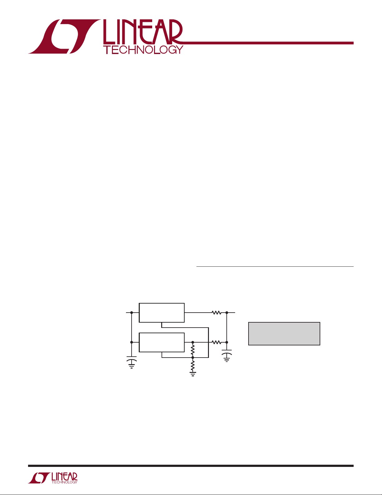
problems. Figure 1 shows a way to use two regulators to
achieve an output current equal to their sum. This circuit
capitalizes on the 1% output tolerance of the specifi ed
regulators to achieve a simple paralleled confi guration.
Both regulators sense from the same divider string and
the small value resistors provide ballast to account for the
slightly differing output voltages. This added impedance
degrades total circuit regulation to about 1%.
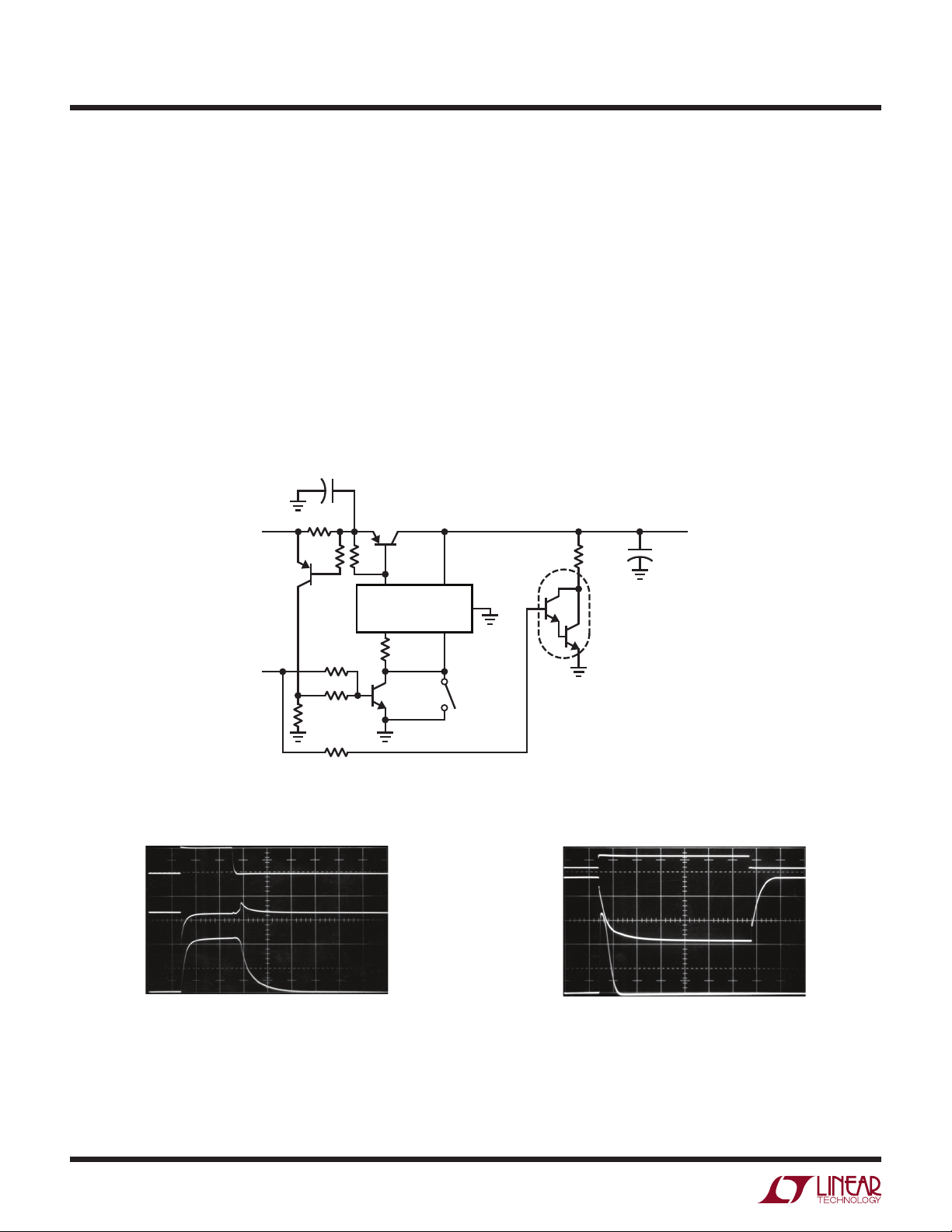
Figure 2 shows another way to extend current capability
in a regulator. Although this circuit is more complex than
Figure 1, it eliminates the ballasting resistor’s effects
and has a fast-acting logic-controlled shutdown feature.
Additionally, the current limit may be set to any desired
®
value. This circuit extends the 1A capacity of the LT
1005
multifunction regulator to 12A, while retaining the LT1005’s
enable feature and auxiliary 5V output. Q1, a booster
transistor, is servo-controlled by the LT1005, while Q2
senses the current dependent voltage across the 0.05Ω
shunt. When the shunt voltage is large enough, Q2 comes
on, biasing Q3 and shutting down the regulator via the
LT1005’s enable pin. The shunt’s value can be selected
for the desired current limit. The 100°C thermo-switch
limits dissipation in Q1 during prolonged short circuits
by disabling the LT1005. It should be mounted on Q1’s
heat sink.
L, LT, LTC, LTM, Linear Technology and the Linear logo are registered trademarks of Linear
Technology Corporation. All other trademarks are the property of their respective owners.
LT1083
IN OUTVIN ≥ 6.5V
ADJ
LT1083
IN
+
100μF
OUT
ADJ
Figure 1
0.01Ω
0.01Ω
121Ω
365Ω
NOTE: THIS CIRCUIT
WILL NOT WORK WITH
LM-TYPE DEVICES
5V
15A
UPDATE
The LT3080 and LT3083
are better for parallel operation
+
200μF
AN02 F01
an2f
AN2-1
Page 2

Application Note 2
Boosted regulator schemes of this type are often poorly
dynamically damped. Such improper loop compensation
results in large output transients for shifts in the load. In
particular, because Q1’s common emitter confi guration
has voltage gain, transients approaching the input voltage
are possible when the load drops out. Here, the 100μF
capacitor damps Q1’s tendency to overshoot, while the
20Ω value provides turn-off bias. The 250μF unit maintains
Q1’s emitter at DC. Figure 3 shows that this “brute force”
compensation works quite well. Normally the regulator
sees no load. When Trace A goes high, a 12A load (regulator output current is Trace C) is placed across the output
terminals. The regulator output voltage recovers quickly,
with minimal aberration.
250μF
+
Q1
2N4398
8.5 MIN
INPUT
ENABLE
“LO”
0.05Ω*
Q2
2N2907
1k
(HEAT SINK)
20Ω
1k
AUXILIARY ENABLE
10k
10k
1k
IN OUT
LT1005 GND
10k
Q3
2N2222
100°C N.0.
THERMO-SWITCH
ON HEAT SINK
While the 100μF output capacitor aids stability, it prevents
the regulator output from dropping quickly when the enable
command is given. Because Q1 cannot sink current, the
100μF unit’s discharge time is load limited. Q4 corrects
this problem, even when there is no load. When the enable
command is given (Trace A, Figure 4) Q3 comes on, cutting off the LT1005 and forcing Q1 off. Simultaneously, Q4
comes on, pulling down the regulator output (Trace B), and
sinks the 100μF capacitor’s discharge current (Trace C). If
fast turn-off is not needed, Q4 may be omitted.
OUTPUT
+
0.05Ω 100μF
Q4
2N6387
*SELECT FOR I LIMIT = 12A
AN02 F02
5V
12A
A = 10V/DIV
B = 0.5V/DIV
AC-COUPLED
C = 5A/DIV
AN2-2
HORIZONTAL = 10μs/DIV
Figure 3
AN02 F03
Figure 2
A = 10V/DIV
B = 2V/DIV
C = 2A/DIV
HORIZONTAL = 100μs/DIV
Figure 4
AN02 F04
an2f
Page 3

Application Note 2
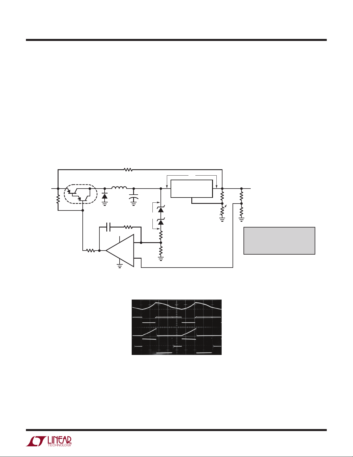
Power dissipation control is another area where regulators
can be helped by additional circuitry. Increasing heat sink
area can be used to offset dissipation problems, but is a
wasteful and ineffi cient approach. Instead, the regulator can
be placed within a switched-mode loop that servo-controls
the voltage across the regulator. In this arrangement the
regulator functions normally while the switched-mode control loop maintains the voltage across it at a minimal value,
regardless of line or load changes. Although this approach
is not quite as effi cient as a classical switching regulator,
it offers lower noise and the fast transient response of
the linear regulator. Figure 5 details a DC driven version
2.2k
Q1
28V
2N6667
INPUT
10k
1k
1N4003
68pF
1MHY
28V
LT1018
1M
+
4500
V
Z
IN
LT1004
1.2
LT1004
2.5
15k
+
10k
–
of the circuit. The LT350A functions in the conventional
fashion, supplying a regulated output at 3A capacity. The
remaining components form the switched-mode dissipation limiting control. This loop forces the potential across
the LT350A to equal the 3.7V value of V
. When the input
Z
of the regulator (Trace A, Figure 6) decays far enough, the
LT1018 output (Trace B) switches low, turning on Q1 (Q1
collector is Trace D). This allows current fl ow (Trace C)
from the circuit input into the 4500μF capacitor, raising
the regulator’s input voltage. When the regulator input
rises far enough, the comparator goes high, Q1 cuts off
and the capacitor ceases charging.
V
Z
LT350A
*1% FILM RESISTOR
1MHY = DALE TD-5 TYPE
OUT
ADJ
2.0k
240Ω* 15k
OUTPUT
10k
UPDATE
The LT3083 allows adjustment
to zero. Various single chip
switching regulators can be used
AN02 F05
A = 100mV/DIV
AC-COUPLED ON
15.7V DC LEVEL
B = 50V/DIV
C = 4A/DIV
D = 20V/DIV
Figure 5
HORIZONTAL = 100μs/DIV
Figure 6
AN02 F06
an2f
AN2-3
Page 4

Application Note 2
The 1N4003 damps the fl yback spike of the current-limiting inductor. The 4.7kΩ unit ensures circuit start-up and
the 68pF-1MΩ combination sets loop hysteresis at about
80mV
. This free-running oscillation control mode
P-P
substantially reduces dissipation in the regulator, while
preserving its performance. Despite changes in the input
voltage, different regulated outputs or load shifts, the
loop always ensures the minimum possible dissipation
in the regulator.
STANCOR
P-8675
110AC
1N4003
82k
10k
20Ω
20Ω
1N4003
†
†
15V
1μF
43
t
t
1
+
2
1k
1MHY
+
1N4003
T1
15V
2
+
C1
LT1011
3
–
4
10,000μF
15V
8
200k
7
1
0.1
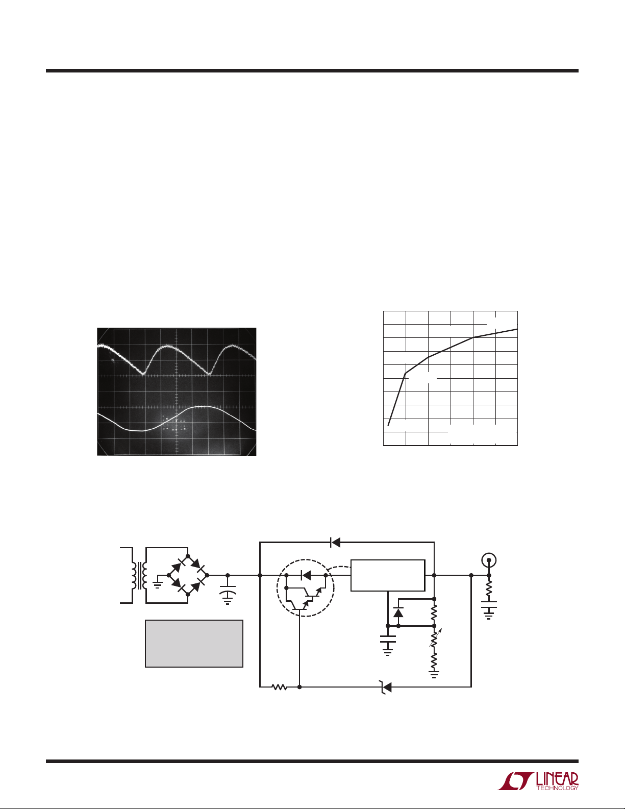
Figure 7 shows the dissipation limiting technique applied
in a more sophisticated circuit. The AC-powered version
provides 0V-35V, 10A regulation under high line-low line
(90VAC-140VAC) conditions with good effi ciency. In this
version, two SCRs and a center-tapped transformer source
power to the inductor-capacitor combination. The transformer output is also diode rectifi ed (Trace A, Figure 8),
divided down, and used to reset the 0.1μF unit (Trace B)
V
Z
0V-35V
0A-10A
(7.5A FOR LT1083)
100μF
LT1004
1.2
LT1004
2.5
16k*
11k*
V
Z
LT1038 OR
LT1083
750Ω*
20k
2.7k
LT1004
1.2V
+
–15V
*1% FILM RESISTOR
T1 = SPRAGUE 11Z-2003
†
SCRs = G.E. C-220B
1MHY = DALE TD-5 TYPE
UPDATE
Paralled LT3083s allow
adjustment to zero
without the LT1004
–15V
15k
1N4148
7
15V
15V
1
8
C2
LT1011
–15V
2N3904
100pF
8
1
A1
LM301A
–15V
15V
+
16k*
–
11k*
AN02 F07
–
3
15V
15k
2
+
4
10k
1μF
Figure 7
AN2-4
an2f
Page 5

Application Note 2
via C1. The resulting AC line synchronous ramp at C1’s
output is compared to A1’s offset output by C2. A1’s output
represents the deviation from the V
value that the loop is
Z
trying to force across the LT1038. When the ramp output
exceeds C2’s “+” input value, C2 pulls low, dumping current
through T1’s primary (Trace C). This fi res the appropriate
SCR and a path from the main transformer to the LC pair
occurs (Trace D). The resultant current fl ow (Trace E) is
limited by the inductor and charges the capacitor. When
the AC line cycle drops low enough, the SCR commutates
and charging ceases. On the next half cycle the process
repeats, except that the alternate SCR does the work. In
this fashion, the loop controls the phase angle at which
the SCRs fi re to keep the voltage across the LT1038 at V
Z
SCR
GATES
TO
(3.7V). As a result, the circuit functions over all line, load
and output voltage conditions with good effi ciency. The
1.2V LT1004 at the LT1038 allows the output voltage to
be set down to 0.00 and the 2N3904 clamp at A1 prevents
loop “hang-up”. Figure 7A shows a way to trigger the SCRs
without using a transformer.
Although A1’s output is an analog voltage, the AC-driven
nature of the circuit makes it approximate a smoothed,
sample loop response. Conversely, the regulator constitutes a true linear system. Because these two feedback
systems are interlocked, frequency compensation can
be diffi cult.
1N4148
20Ω
20Ω
10k
1MHY
10,000μF
TO 10k-15k JUNCTION
FROM A1 OUTPUT
C1 OUTPUT
A = 50V/DIV
B = 10V/DIV
C = 100mA/DIV
D = 50V/DIV
E = 10A/DIV
15V 15V
–
3
C2
2
TO
+
10k
2N2219
1N4148
0.68
AN02 F07A
Figure 7A
HORIZONTAL = 2ms/DIV
AN02 F08
Figure 8
an2f
AN2-5
Page 6

Application Note 2
In practice, A1’s 1μF capacitor keeps dissipation loop
gain at a low enough frequency for stable characteristics,
without infl uencing the LT1038’s transient response characteristic. Trace A, Figure 9 shows the output noise while
the circuit is operating at 35V into a 10A load (350W). Note
the absence of fast switching transients and harmonics.
The output noise is made up of residual 120Hz ripple and
regulator noise. Refl ected noise into the AC power line is
also negligible (Trace B) because the inductor limits current rise time to about 1ms, much slower than the normal
switching supplies. Figure 10 shows a plot of effi ciency
versus output voltage for a 10A load. At low output voltages, where the static losses across the regulator and SCRs
are signifi cant, effi ciency suffers, but 85% is attained at
the upper extreme.
10mV/DIV
AC-COUPLED
ON 35V OUTPUT
200V/DIV
HORIZONTAL = 2ms/DIV
Figure 9
AN02 F09
High voltage output is another area for regulator enhancement. In theory, because the regulator does not have a
ground pin, it can regulate high voltages. In normal operation the regulator fl oats at the supply’s upper level, and as
long as the V
IN–VOUT
maximum differential is not exceeded
there are no problems. However, if the output is shorted,
the V
IN–VOUT
maximum is exceeded and device destruction will occur. The circuit of Figure 11 shows a complete
high voltage regulator that delivers 100V at 100mA and
withstands shorts to ground. Even at 100V output the
LT317A functions in the normal mode, maintaining 1.2V
between its output and adjustment pin.
100
90
80
70
P = 100W
60
50
40
EFFICIENCY (%)
30
20
P = 10W
10
0
0
P = 50W
5
10
OUTPUT VOLTAGE
P = 200W
LOAD CURRENT = 10A
FOR ALL CONDITIONS
15 20
Figure 10
P = 300W
25
AN02 F10
30
AN2-6
115AC
TRIAD
N-48X
1N4004
UPDATE
Newer regulators such as
the LT3080 and LT3081
allow adjustment to zero
1N4004
≈120V
+
500μF
2k
5W
Q1
2N6533
LT317AT
IN
1N3031
30V
ADJ
500pF
OUT
1N4148 332Ω
1k
OUTPUT
ADJ
25.5k
100V
OUTPUT
10Ω
0.02μF
AN02 F11
Figure 11
an2f
Page 7

Application Note 2
Under these conditions the 30V Zener is off and Q1 conducts. When an output short occurs, the Zener conducts,
forcing Q1’s base to 30V. This causes Q1’s emitter to clamp
s below VZ, well within the VIN–V
2 V
BE
rating of the
OUT
regulator. Under these conditions, Q1, a high voltage device,
sustains 90V V
at whatever current the transformer and
CE
the regulator’s current limit will support. The transformer
specifi ed saturates at 130mA, keeping Q1 well within its
safe area as it dissipates 12W. If Q1 and the LT317A are
thermally coupled, the regulator will soon go into thermal
shutdown and oscillation will commence. This action will
continue, protecting the load and the regulator as long as
the output remains shorted. the 500pF capacitor and the
10Ω-0.02μF damper aid transient response and the diodes
provide safe discharge paths for the capacitors.
This approach to high voltage regulation is primarily limited by the power dissipation capability of the device in
series with the regulator. Figure 11A uses a vacuum tube
(remember them?) to achieve very high short-circuit dissipation capability. The tube allows high voltage operation
and is extremely tolerant of overloads. This circuit allows
the LT317A to control 600W at 2000V (V1’s plate limit is
300mA) with full short-circuit protection.
Power is not the only area in which regulator performance
can be augmented. Figure 12 shows a way to increase the
stability of a regulator’s output over time and temperature.
This is particularly useful in powering strain gauge-based
transducers. In this circuit the output voltage is divided
down and compared to the 2.5V reference by A1, a precision
amplifi er. A1’s output is used to force the LT317A’s adjustment pin to whatever voltage is required to maintain the
10V output. A1 contributes negligible error. The resistors
specifi ed will track within 5ppm/°C and the reference contributes about 20ppm/°C. The regulator’s internal circuitry
protects against short circuits and thermal overload.
Figure 13’s circuit allows a regulator to remotely sense the
feedback voltage, eliminating the effects of voltage drop
in the supply lines. This is a concern where high currents
must be transmitted over relatively long supply rails or PC
traces. Figure 13’s circuit uses A1 to sense the voltage at
the point of load. A1’s output, summed with the regulator’s
output, modifi es the adjustment pin voltage to compensate
for the voltage lost across R
. The feedback divider is
DROP
returned through a separate lead from the load, completing the remote sensing scheme. The 5μF capacitor fi lters
noise and the 1k value limits bypass capacitor discharge
when power is turned off.
2500V
75-TH
FILIMENT
EIMAC
180k
50W
UPDATE
The LT3085 will allow
V
to go to zero
OUT
1N3031
V1
500k
OUTPUT
TRIM
AN02 F11A
OUTPUT
2000V
LT317AH
INV
IN
ADJ
OUT
2k
A1
LT1001
LT317AT
IN
OUT
ADJ
1.2k
1.8M
2W
Figure 11A Figure 12
+
–
LT1009
2.5V
OUTPUT
10V
2k 15k*
4.99k**RESISTORS = TRW MAR-6
AN02 F12
Information furnished by Linear Technology Corporation is believed to be accurate and reliable.
However, no responsibility is assumed for its use. Linear Technology Corporation makes no representation that the interconnection of its circuits as described herein will not infringe on existing patent rights.
an2f
AN2-7
Page 8

Application Note 2
A fi nal circuit allows voltage regulator-powered circuity to
run from 110VAC or 220VAC without having to switch transformer windings. Regulator dissipation does not increase
for 220VAC inputs. In Figure 14, when T1 is driven from
110VAC, the LT1011 output goes high, allowing the SCR
to receive gate bias through the 1.2k resistor. The 1N4002
is off. T1’s output is rectifi ed by the SCR and the regulator
sees about 8.5V at its input. If T1 is plugged into a 220VAC
source, the negative input at the LT1011 is driven beyond
2.5V and the device’s output clamps low. This steers the
SCR’s gate bias to ground through the LT1011’s output
transistor. The diodes in the LT1011 output line prevent
INV
IN
LT350A
OUT
ADJ
22Ω
121Ω
365Ω
Figure 13
reverse voltages from reaching the SCR or the LT1011
output. Now, the SCR goes off and the 1N4002 sources
current to the regulator from T1’s center tap. Although
T1’s input voltage has doubled, its output potential has
halved and the regulator power dissipation remains the
same. Figure 15 shows the AC line input versus regulator
input voltage transfer function. The switch to center tap
drive occurs midway between 110VAC and 220VAC. The
hysteresis, a desirable characteristic, occurs because T1’s
output voltage shifts with the step change in loading.
R
DROP
(MAX DROP = 300mV)
V
IN
–
A1
LM301A
1
100pF
+
8
4
1k
25Ω
5μF
+
5V AT 3A
R
LOAD
AN02 F13
HIGH CURRENT
RETURN
TO GROUND
110-220AC
1.6k
1k
1M
1μF
AN2-8
3
–
2
+
LT1009C
2.5V
C-106 (G.E.)
T1
LT1011
4
8
1N4002
1.2k
7
1
+
5000μF
1k
6.2k
LT1086
IN
ADJ
*1% FILM RESISTOR
T1 = STACO #SP05A012
= 1N4148 UNLESS MARKED
UPDATE
The LT3080 regulator
allows V
OUT
Figure 14
Linear Technology Corporation
1630 McCarthy Blvd., Milpitas, CA 95035-7417
(408) 432-1900 ● FAX: (408) 434-0507
●
www.linear.com
OUT
to go to zero
240Ω*
720Ω*
AN02 F14
V
OUT
10μF
5V
18
16
14
12
10
8
6
4
REGULATOR INPUT VOLTAGE
2
0
0
80
40
120 280
AC LINE VOLTAGE—RMS
160
200 240
AN02 F15
+
Figure 15
an2f
GP/IM 286 5K • PRINTED IN USA
© LINEAR TECHNOLOGY CORPORATION 1986
 Loading...