

Page 1

Some Thoughts on DC/DC Converters
Jim Williams and Brian Huffman
INTRODUCTION
Application Note 29
October 1988
Many systems require that the primary source of DC power
be converted to other voltages. Battery driven circuitry is
an obvious candidate. The 6V or 12V cell in a laptop computer must be converted to different potentials needed for
memory, disc drives, display and operating logic. In theory,
AC line powered systems should not need DC/DC converters
because the implied power transformer can be equipped
with multiple secondaries. In practice, economics, noise
requirements, supply bus distribution problems and other
constraints often make DC/DC conversion preferable. A
common example is logic dominated, 5V powered systems
utilizing ±15V driven analog components.
The range of applications for DC/DC converters is large,
with many variations. Interest in converters is commensurately quite high. Increased use of single supply powered
systems, stiffening performance requirements and battery
operation have increased converter usage.
Historically, effi ciency and size have received heavy emphasis. In fact, these parameters can be signifi cant, but
often are of secondary importance. A possible reason
behind the continued and overwhelming attention to size
and effi ciency in converters proves surprising. Simply
put, these parameters are (within limits) relatively easy to
achieve! Size and effi ciency advantages have their place,
but other system-oriented problems also need treatment.
Low quiescent current, wide ranges of allowable inputs,
substantial reductions in wideband output noise and cost
effectiveness are important issues. One very important
converter class, the 5V to ±15V type, stresses size and
effi ciency with little emphasis towards parameters such
as output noise. This is particularly signifi cant because
wideband output noise is a frequently encountered problem
with this type of converter. In the best case, the output noise
mandates careful board layout and grounding schemes.
In the worst case, the noise precludes analog circuitry
from achieving desired performance levels (for further
discussion see Appendix A, “The 5V to ±15V Converter
— A Special Case”). The 5V to ±15V DC/DC conversion
requirement is ubiquitous, and presents a good starting
point for a study of DC/DC converters.
5V TO ±15V CONVERTER CIRCUITS
Low Noise 5V to ±15V Converter
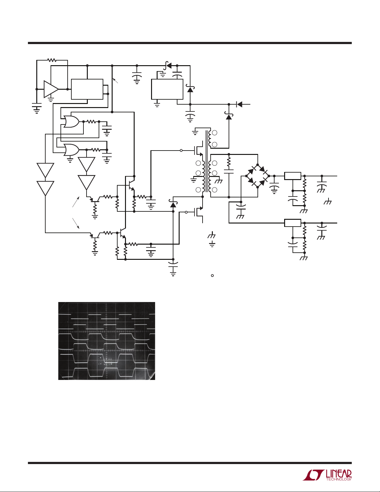
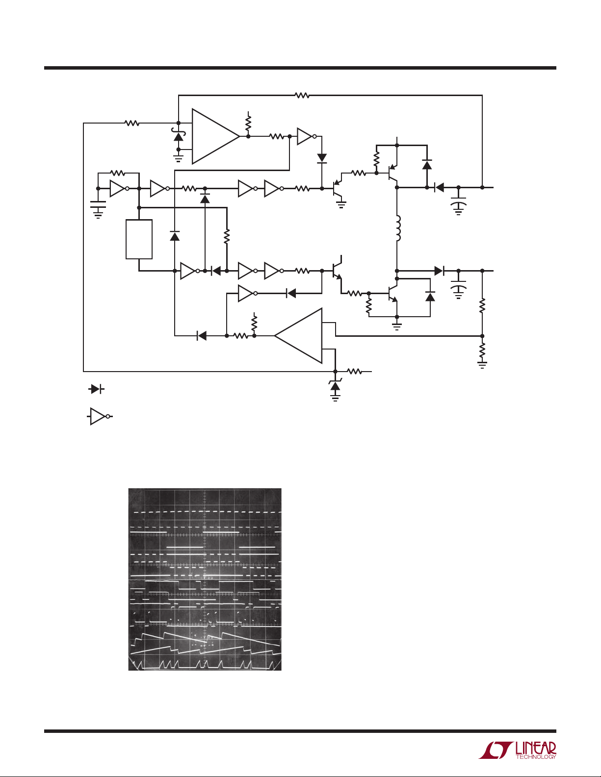
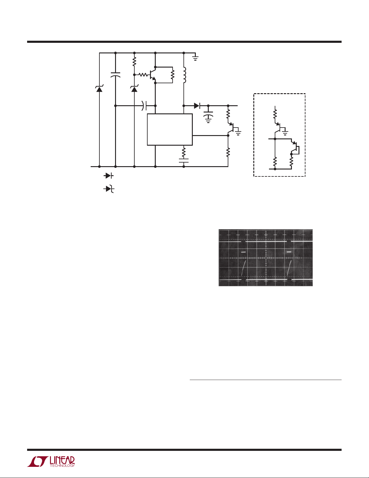
Figure 1’s design supplies a ±15V output from a 5V input.
Wideband output noise measures 200 microvolts peakto-peak, a 100× reduction over typical designs. Effi ciency
at 250mA output is 60%, about 5% to 10% lower than
conventional types. The circuit achieves its low noise
performance by minimizing high speed harmonic content
in the power switching stage. This forces the effi ciency
trade-off noted, but the penalty is small compared to the
benefi t.
The 74C14 based 30kHz oscillator is divided into a 15kHz
2-phase clock by the 74C74 fl ip-fl op. The 74C02 gates and
10k-0.001μF delays condition this 2-phase clock into nonoverlapping, 2-phase drive at the emitters of Q1 and Q2
(Figure 2, Traces A and B, respectively). These transistors
provide level shifting to drive emitter followers Q3-Q4. The
Q3-Q4 emitters see 100Ω-0.003μF fi lters, slowing drive
to output MOSFETs Q5-Q6. The fi lter’s effects appear at
the gates of Q5 and Q6 (Traces C and D, respectively). Q5
and Q6 are source followers, instead of the conventional
common source connection. This limits transformer rise
time to the gate terminals fi ltered slew rate, resulting in
L, LT, LTC, LTM, Linear Technology and the Linear logo are registered
trademarks of Linear Technology Corporation. All other trademarks are the
property of their respective owners.
an32f
AN29-1
Page 2
Application Note 29
0.001
CLK-NON
OVERLAP
GENERATOR
22k
74C14
74C02
74C14
74C14
CK
74C02
15kHz, 5μs
NON-OVERLAP
+V
74C74
Q
10k
10k
74C14
74C14
K1
Q1
LEVEL SHIFTS
K2
Q2
Q
D
0.001
0.001
100Ω
150k 1k
10k
100Ω
10k
+
POINT
“A”
(SEE TEXT)
BOOST
OUTPUT
≈17V
DC
DIRVERS-
EDGE
SHAPING
Q4
100
1k150k
1N5817
+
2
8
–4V
+
10
+
D1
1N5817
DC
22μF
Q5
1N5817
47
4
5V
D
6
S
1
7
2
8
3 9
L1
OUTPUT
S
Q6
D
5V
= ±15 COMMON
= +5 GROUND
* = 1% FILM RESISTOR
FET = MTP3055E-MOTOROLA
PNP = 2N3906
NPN = 2N3904
L1 = PULSE ENGINEERING, INC. #PE-61592
= FERRITE BEAD, FERRONICS #21-110J
D3
1N5817
D2
1N5817
TURBO BURST
470
0.001
100μF
+
5V
IN
(4.5V TO 5.5V)
MUR 120
(ALL)
10μF
1μF
+
+15
OUT
OUT
COMMON
–15
OUT
LT1086
+
100μF
+
10μF
LT337A
10μF
+
124*
1.37k*
249*
2.74k*
AN29 F01
+
100
3
LT1054
5
BOOST
Q3
100
0.003
0.003
Figure 1. Low Noise 5V to ±15V Converter
A = 20V/DIV
B = 20V/DIV
C = 20V/DIV
D = 20V/DIV
E = 10V/DIV
F = 10V/DIV
HORIZ = 20μs/DIV
AN29 F02
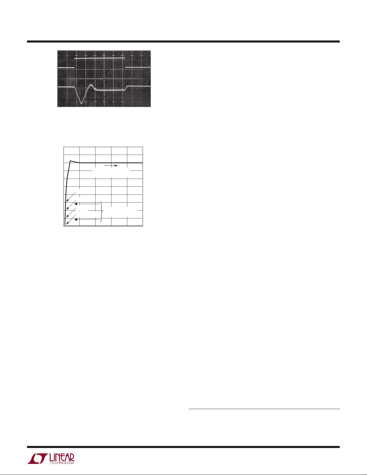
Figure 2. 5V to ±15V Low Noise Converter Waveforms
well controlled waveforms at the sources of Q5 and Q6
(Traces E and F, respectively). L1 sees complimentary,
slew limited drive, eliminating the high speed harmonics
normally associated with this type converter. L1’s output
is rectifi ed, fi ltered and regulated to obtain the fi nal out-
put. The 470Ω-0.001μF damper in L1’s output maintains
loading during switching, aiding low noise performance.
The ferrite beads in the gate leads eliminate parasitic RF
oscillations associated with follower confi gurations.
The source follower confi guration eases controlling L1’s
edge rise times, but complicates gate biasing. Special
provisions are required to get the MOSFETs fully turned
on and off. Source follower connected Q5 and Q6 require
voltage overdrive at the gates to saturate. The 5V primary
supply cannot provide the specifi ed 10V gate — channel
bias required for saturation. Similarly, the gates must be
pulled well below ground to turn the MOSFETs off. This
is so because L1’s behavior pulls the sources negative
when the devices turn off. Turn-off bias is bootstrapped
from the negative side of Q6’s source waveform. D1 and
the 22μF capacitor produce a –4V potential for Q3 and Q4
to pull down to. Turn-on bias is generated by a 2-stage
an32f
AN29-2
Page 3
Application Note 29
boost loop. The 5V supply is fed via D3 to the LT®1054
switched capacitor voltage converter (switched capacitor
voltage converters are discussed in Appendix B, “Switched
Capacitor Voltage Converters — How They Work”). The
LT1054 confi guration, set up as a voltage doubler, initially
provides about 9V boost to point “A” at turn-on. When
the converter starts running L1 produces output (“Turbo
Boost” on schematic) at windings 4-6 which is rectifi ed by
D2, raising the LT1054’s input voltage. This further raises
point “A” to the 17V potential noted on the schematic.
These internally generated voltages allow Q5 and Q6 to
receive proper drive, minimizing losses despite their source
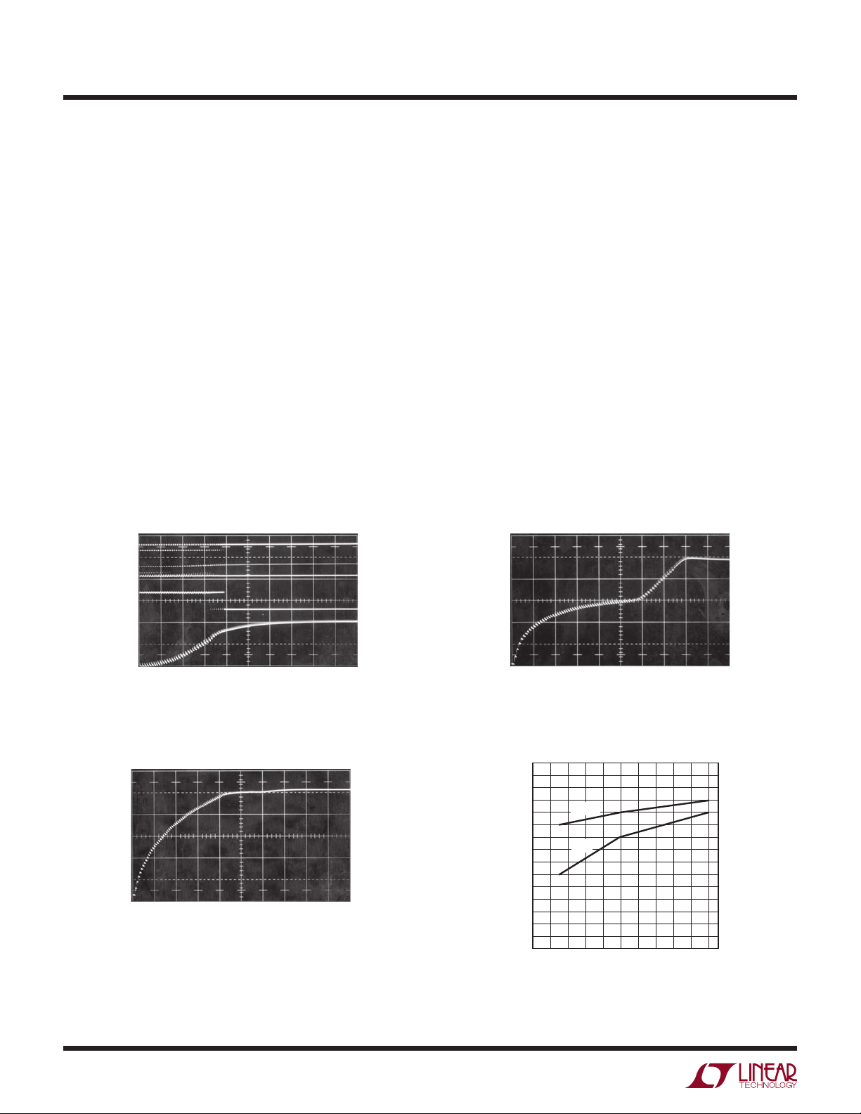
follower connection. Figure 3, an AC-coupled trace of the
15V converter output, shows 200μV
noise at full power
P-P
(250mA output). The –15V output shows nearly identical characteristics. Switching artifacts are comparable in
amplitude to the linear regulators noise. Further reduction
in switching based noise is possible by slowing Q5 and
Q6 rise times. This, however, necessitates reducing clock
rate and increasing non-overlap time to maintain available
output power and effi ciency. The arrangement shown
represents a favorable compromise between output noise,
available output power, and effi ciency.
A = 100μV/DIV
(AC-COUPLED)
less than 30μV of output noise. This is almost 7× lower
than the previous circuit and approaches a 1000× improvement over conventional designs. The trade off is effi ciency
and complexity.
A1 is set up as a 16kHz Wein bridge oscillator. The single
power supply requires biasing to prevent A1’s output from
saturating at the ground rail. This bias is established by
returning the undriven end of the Wein network to a DC
potential derived from the LT1009 reference. A1’s output
is a pure sine wave (Figure 5, Trace A) biased off ground.
A1’s gain must be controlled to maintain sine wave output.
A2 does this by comparing A1’s rectifi ed and fi ltered positive output peaks with an LT1009 derived DC reference.
A2’s output, biasing Q1, servo controls A1’s gain. The
0.22μF capacitor frequency compensates the loop, and the
thermally mated diodes minimize errors due to rectifi er
temperature drift. These provisions fi x A1’s AC and DC
output terms against supply and temperature changes.
A1’s output is AC coupled to A3. The 2k –820Ω divider
re-biases the sine wave, centering it inside A3’s input
common mode range even with supply shifts. A3 drives a
power stage, Q2-Q5. The stages common emitter outputs
and biasing permit 1V
at V
= 4.5V. At full converter output loading the
SUPPLY
RMS
(3V
) transformer drive, even
P-P
stage delivers 3 ampere peaks but the waveform is clean
(Trace B), with low distortion (Trace C). The 330μF coupling
capacitor strips DC and L3 sees pure AC. Feedback to A3 is
taken at the Q4-Q5 collectors. The 0.1μF unit at this point
suppresses local oscillations. L3’s secondary RC network
adds additional high frequency damping.
HORIZ = 5μs/DIV
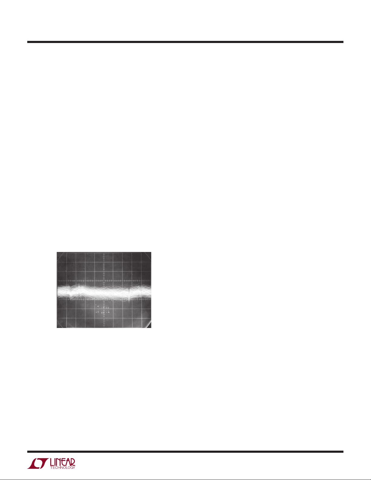
Figure 3. Output Noise of the Low Noise 5V to ±15V Converter.
Appendix H Shows a Modern IC Low Noise Regulator
AN29 F03
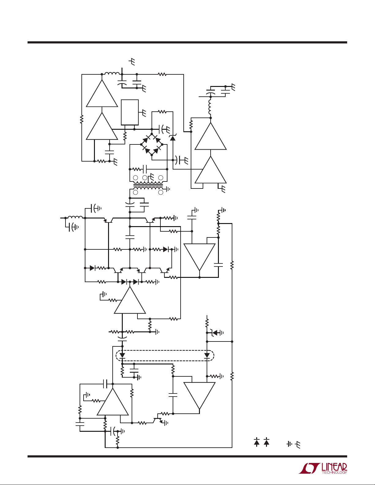
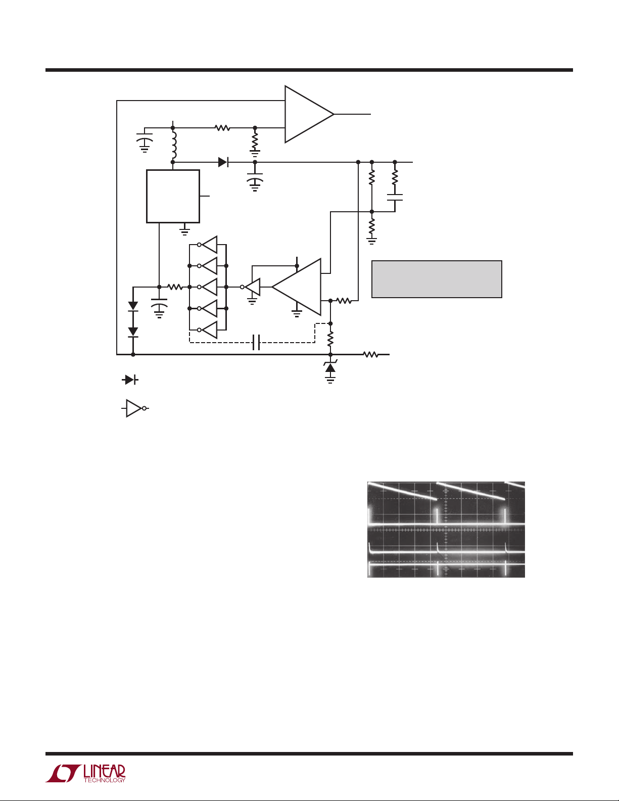
Ultralow Noise 5V to ±15V Converter
Residual switching components and regulator noise set
Figure 1’s performance limits. Analog circuitry operating
at the very highest levels of resolution and sensitivity may
require the lowest possible converter noise. Figure 4’s
converter uses sine wave transformer drive to reduce
harmonics to negligible levels. The sine wave transformer
drive combines with special output regulators to produce
Without control of quiescent current the power stage
will encounter thermal runaway and destroy itself. A4
measures DC output current across Q5’s emitter resistor
and servo controls Q6 to fi x quiescent current. A divided
portion of the LT1009 reference sets the servo point at
A4’s negative input and the 0.33μF feedback capacitor
stabilizes the loop.
L3’s rectifi ed and fi ltered outputs are applied to regulators
designed for low noise. A5 and A7 amplify the LT1021’s
fi ltered 10V output up to 15V. A6 and A8 provide the –15V
output. The LT1021 and amplifi ers give better noise performance than three terminal regulators. The Zener-resistor
network clips overvoltages due to start-up transients.
an32f
AN29-3
Page 4
Application Note 29
OUT
15V
L1
25μH
+
47μF
A7
LT1010
IN
5V
(4.5V TO 5.5V)
4.99k*
A5
–
1/2 LT1013
10k*
22μF
+
L4
100μH
Q4
+
22μF
1N4001
68Ω
AMP
POWER
430Ω
8
+
1μF
MJE2955
50Ω
Q2
OUT
5k
†
330μF
0.1
2N2219
0.1
LT1021
L3
+
OUT
10V
IN
330Ω
534
8
0.1
50Ω
Q3
COMMON
19V
UNREG
*
*
0.005
Q5
MJE3055
2N2905
220μF
+
*
*
1
100Ω
330Ω 10k*
1N4001
Q6
0.1Ω
220μF
10k
1k750Ω*
10k*
1N5260B
+
–19V
UNREG
0.22
+
47μF
OUT
–15V
L2
25μH
A8
LT1010
4
A6
–
1/2 LT1013
620Ω
Q
I
LOOP
CONTROL
10k
–
+
A4
1/2 LT1013
0.33
AN29 F04
0.1
+
20k
0.01
LT1006
270Ω
–
1k*
(SELECTED
VALUE—
SEE TEXT)
430Ω
5V
1k
LT1009
2.5
MATED
THERMALLY
200k
–
0.22
2k
Q1
1/2 LT1013
A2
+
OSCILLATOR
10k
STAB. LOOP
3.1k
= 1N4148
= 1N4934
L1, L2 = PULSE ENGINEERING, INC. #PE-92100
L3 = PULSE ENGINEERING, INC. #PE-65064
*
L4 = PULSE ENGINEERING, INC. #PE-92108
= THF337K006P1G
UNMARKED NPN = 2N3904
* = 1% METAL FILM RESISTOR
†
= +5 GROUND
= ±15 COMMON
Figure 4. Ultralow Noise Sine Wave Drive 5V to ±15V Converter
an32f
220Ω
8
A3
+
820Ω
2k
5V
1μF
+
10k
A1
LT1006
47μF
0.22
680Ω
–
220Ω
0.01
8
+
1k
16kHz
OSCILLATOR
1k
+
1k
AN29-4
Page 5
A = 2V/DIV
B = 2V/DIV
C = 1% DISTORTION
D = 20μV/DIV
HORIZ = 50μs/DIV
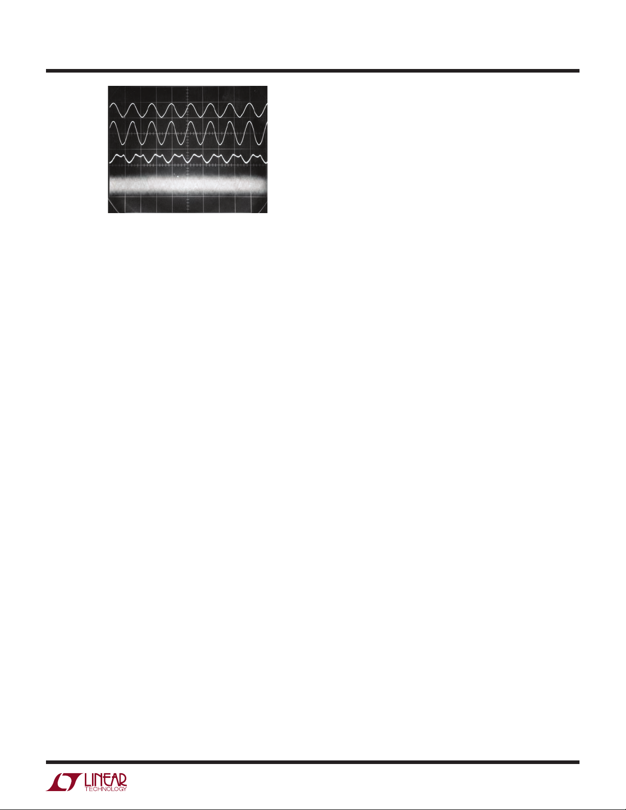
Figure 5. Waveforms for the Sine Wave Driven Converter.
Note that Output Noise (Trace D) is Only 30μV
AN29 F05
P-P
L1 and L2 combine with their respective output capacitors to aid low noise characteristics. These inductors are
outside the feedback loop, but their low copper resistance
does not signifi cantly degrade regulation. Trace D, the 15V
output at full load, shows less than 30μV (2ppm) of noise.
The most signifi cant trade-off in this design is effi ciency.
The sine wave transformer drive forces substantial power
loss. At full output (75mA), effi ciency is only 30%.
Before use, the circuit should be trimmed for lowest
distortion (typically 1%) in the sine wave delivered to
L3. This trim is made by selecting the indicated value at
A1’s negative input. The 270Ω value shown is nominal,
with a typical variance of ±25%. The sine wave’s 16kHz
frequency is a compromise between the op amps available gain bandwidth, magnetics size, audible noise, and
minimization of wideband harmonics.
Single Inductor 5V to ±15V Converter
Simplicity and economy are another dimension in 5V to
±15V conversion. The transformer in these converters is
usually the most expensive component. Figure 6’s unusual
drive scheme allows a single, 2-terminal inductor to replace
the usual transformer at signifi cant cost savings. Tradeoffs include loss of galvanic isolation between input and
output and lower power output. Additionally, the regulation
technique employed causes about 50mV of clock related
output ripple.
The circuit functions by periodically and alternately allowing
each end of the inductor to fl yback. The resultant positive
and negative peaks are rectifi ed and fi ltered. Regulation
is obtained by controlling the number of fl yback events
during the respective output’s fl yback interval.
Application Note 29
The leftmost logic inverter produces a 20kHz clock (Trace A,
Figure 7) which feeds a logic network composed of additional inverters, diodes and the 74C90 decade counter. The
counter output (Trace B) combines with the logic network
to present alternately phased clock bursts (Traces C andD)
to the base resistors of Q1 and Q2. When φ1 (Trace B)
is unclocked it resides in its high state, biasing Q2 and
Q4 on. Q4’s collector effectively grounds the “bottom” of
L1 (TraceH). During this interval φ2 (Trace A) puts clock
bursts into Q1’s base resistor. If the –15V output is too
low servo comparator C1A’s output (Trace E) is high, and
Q1’s base can receive pulsed bias. If the converse is true
the comparator will be low, and the bias gated away via
Q1’s base diode. When Q1 is able to bias, Q3 switches,
resulting in negative going fl yback events at the “top” of
L1 (Trace G). These events are rectifi ed and fi ltered to
produce the –15V output. C1A regulates by controlling
the number of clock pulses that switch the Q1-Q3 pair.
The LT1004 serves as a reference. Trace J, the AC-coupled
–15V output, shows the effect of C1A’s regulating action.
The output stays within a small error window set by C1A’s
switched control loop. As input voltage and loading conditions change C1A adjusts the number of clock pulses
allowed to bias Q1-Q3, maintaining loop control.
When the φ1 and φ2 signals reverse state the operating
sequence reverses. Q3’s collector (Trace G) is pulled high
with Q2-Q4 switching controlled by C1B’s servo action.
Operating waveforms are similar to the previous case.
Trace F is C1B’s output, Trace H is Q4’s collector (L1’s “bottom”) and Trace I is the AC-coupled 15V output. Although
the two regulating loops share the same inductor they
operate independently, and asymmetrical output loading is
not deleterious. The inductor sees irregularly spaced shots
of current (Trace K), but is unaffected by its multiplexed
operation. Clamp diodes prevent reverse biasing of Q3
and Q4 during transient conditions. The circuit provides
±25mA of regulated power at 60% effi ciency.
Low Quiescent Current 5V to ±15V Converter
A fi nal area in 5V to ±15V converter design is reduction
of quiescent current. Typical units pull 100mA to 150mA
of quiescent current, unacceptable in many low power
systems.
an32f
AN29-5
Page 6
Application Note 29
150k*
12.4k*
HP5082-2810
32k
1000pF
5
74C90
÷10
12
= 1N4148
* = 1% METAL FILM RESISTOR
= 74C14
+
1/2 LT1018
–
10k
C1A
10k
10k
5V
300Ω
10k
100Ω
K2
4.7k
K1
4.7k
5V
300Ω
C1B
1/2 LT1018
Q1
2N3906
5V
Q2
2N3904
100Ω
+
–
1k
LT1004
1.2V
5V
2k
Q3
2N5023
–15V
15V
137k*
12.4k*
AN29 F06
OUT
OUT
+
100
L1
145μH
+
Q4
2N3507
2k
5V
100
L1 = PULSE ENGINEERING, INC. # PE-92105
Figure 6. Single Inductor 5V to ±15V Regulated Converter
A = 5V/DIV
B = 5V/DIV
C = 10V/DIV
D = 10V/DIV
E = 10V/DIV
F = 10V/DIV
G = 20V/DIV
H = 20V/DIV
I = 0.05V/DIV (AC-COUPLED)
J = 0.05V/DIV (AC-COUPLED)
K = 1A/DIV
HORIZ = 100μs/DIV
Figure 7. Waveforms for the Single Inductor, Dual-Output,
Regulated Converter
AN29 F07
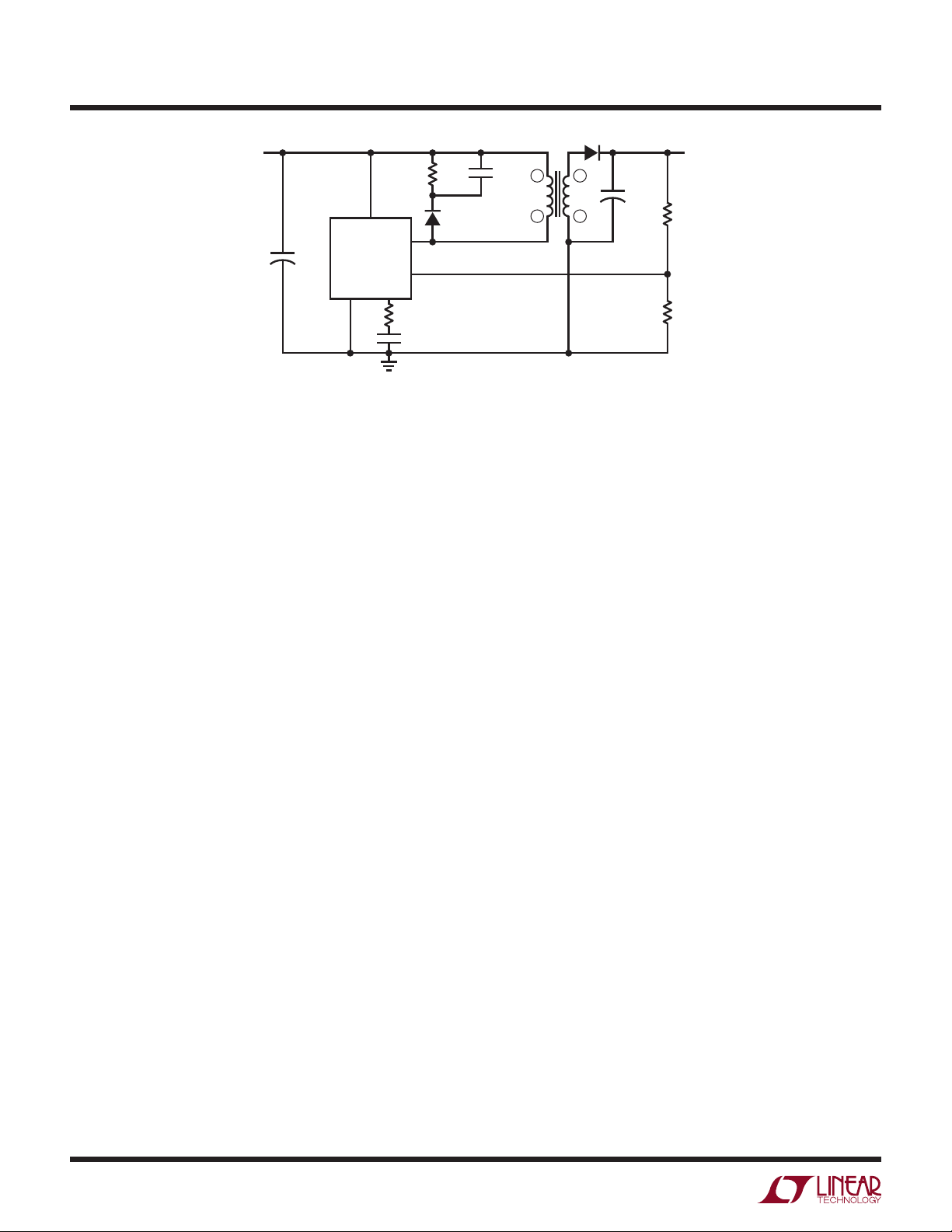
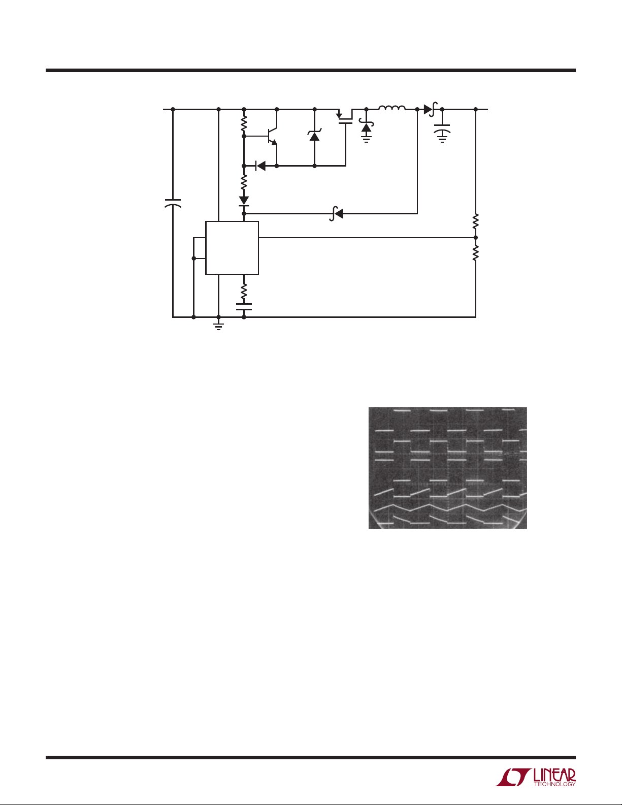
Figure 8’s design supplies ±15V outputs at 100mA while
consuming only 10mA quiescent current. The LT1070
switching regulator (for a complete description of this
device, see Appendix C, “Physiology of the LT1070”) drives
L1 in fl yback mode. A damper network clamps excessive
fl yback voltages. Flyback events at L1’s secondary are
half-wave rectifi ed and fi ltered, producing positive and
negative outputs across the 47μF capacitors. The positive
16V output is regulated by a simple loop. Comparator
C1A balances a sample of the positive output with a 2.5V
reference obtained from the LT1020. When the 16V output (Trace A, Figure 9) is too low, C1A switches (TraceB)
high, turning off the 4N46 opto-isolator. Q1 goes off, and
the LT1070’s control pin (V
causes full duty cycle 40kHz switching at the V
) pulls high (Trace C). This
C
pin
SW
(Trace D). The resultant energy into L1 forces the 16V
output to ramp quickly positive, turning off C1A’s output.
an32f
AN29-6
Page 7

5V
IN
(4.5V TO 5.5V)
Application Note 29
16V PRE-REG
0.47
V
GND
10k
1 9
3 7
SW
1.2k
2W
MUR120
V
IN
NC
2N3906
LT1070FB
V
C
Q1
L1 = PULSE ENGINEERING, INC. # PE-61592
* = 1% FILM RESISTOR
= +5 GROUND
= ±15 COMMON
1N4148
L1
+
8
+
1N4148
5V
4N46
390k
47μF
47μF
1.2M*
82k
216k*
–
C1A
1/2 LT1017
+
20M
10k
–16V UNREG
10k
0.002
UPDATE
Burst Mode regulators
can achieve lower I
Figure 8. Low I
, Isolated 5V to ±15V Converter
Q
Q
9
3
V
GND
–1N
5
COMP
PNP
0.001μF
3M* 500k* 100k
470k
IN
LT1070
2.5V
+IN
REF OUT
74 6
Q2
VN2222
OPTIONAL
(SEE TEXT)
28
OUT
11
FB
COMP
NPN
–16V UNREG
–15V
15V
OUT
2.5M*
0.001μF
100mA
+
500k*
10μF
+
10μF
–15V
OUT
100mA
TO
REF OUT
470k
3.2M
1.5M
–
1/2 LT1017
+
47k
C1B
TO
TO
TO 16V
PRE-REG
1.5k
5.6M
AN29 F08
A = 100mV/DIV
(AC-COUPLED ON
LEVEL)
16V
DC
B = 20V/DIV
C = 2V/DIV
D = 20V/DIV
HORIZ = 5ms/DIV
AN29 F09
Figure 9. Waveforms for the Low IQ 5V to ±15V Converter
The 20M value combined with the 4N46’s slow response
(note the delay between C1A going high and the V
pin
C
rise) gives about 40mV of hysteresis. The LT1070’s onoff duty cycle is load dependent, saving signifi cant power
when the converter is lightly loaded. This characteristic
is largely responsible for the 10mA quiescent current.
The opto-isolator preserves the converters input-output
isolation. The LT1020, a low quiescent current regulator
with low dropout, further regulates the 16V line, giving
the 15V output. The linear regulation eliminates the 40mV
ripple and improves transient response. The –16V output
tends to follow the regulated –16V line, but regulation
is poor. The LT1020’s auxiliary onboard comparator is
compensated to function as an op amp by the RC damper
at Pin 5. This amplifi er linearly regulates the –16V line.
MOSFET Q2 provides low dropout current boost, sourcing
the –15V output. The –15V output is stabilized with the
op amp by comparing it with the 2.5V reference via the
500k-3M current summing resistors. 1000pF capacitors
frequency compensate each regulating loop. This converter
functions well, providing ±15V outputs at 100mA with
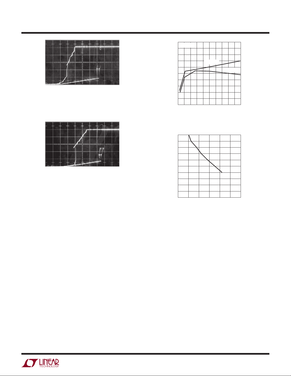
only 10mA quiescent current. Figure 10 plots effi ciency
versus a conventional design over a range of loads. For
high loads results are comparable, but the low quiescent
circuit is superior at lower current.
A possible problem with this circuit is related to the poor
regulation of the –16V line. If the positive output is lightly
loaded L1’s magnetic fl ux is low. Heavy negative output
loading under this condition results in the –16V line falling
below its output regulators dropout value. Specifi cally, with
no load on the 15V output only 20mA is available from
the –15V output. The full 100mA is only available from
an32f
AN29-7
Page 8
Application Note 29
100
90
80
70
60
50
40
EFFICIENCY (%)
30
20
10
0
0
LOW QUIESCENT
CURRENT DESIGN
CONVENTIONAL
DESIGN
2010
4030
50
OUTPUT CURRENT (mA)
60 70 90
80
100
AN29 F10
Figure 10. Effi ciency vs Load for the Low IQ Converter
the –15V output when the 15V output is supplying more
than 8mA. This restriction is often acceptable, but some
situations may not tolerate it. The optional connection in
Figure 8 (shown in dashed lines) corrects the diffi culty.
C1B detects the onset of –16V line decay. When this occurs its output pulls low, loading the 16V line to correct
the problem. The biasing values given permit correction
before the negative linear regulator drops out.
MICROPOWER QUIESCENT CURRENT CONVERTERS
Many battery-powered applications require very wide
ranges of power supply output current. Normal conditions
require currents in the ampere range, while standby or
“sleep” modes draw only microamperes. A typical laptop
computer may draw 1 to 2 amperes running while needing only a few hundred microamps for memory when
turned off. In theory, any DC/DC converter designed
for loop stability under no-load conditions will work. In
practice, a converter’s relatively large quiescent current
may cause unacceptable battery drain during low output
current intervals.
Figure 11 shows a typical fl yback based converter. In this
case the 6V battery is converted to a 12V output by the
inductive fl yback voltage produced each time the LT1070’s
pin is internally switched to ground (for commentary
V
SW
on inductor selection in fl yback converters see Appendix D,
“Inductor Selection for Flyback Converters”). An internal
40kHz clock produces a fl yback event every 25μs. The
energy in this event is controlled by the IC’s internal error amplifi er, which acts to force the feedback (FB) pin to
a 1.23V reference. The error amplifi ers high impedance
output (the VC pin) uses an RC damper for stable loop
compensation.
This circuit works well but pulls 9mA of quiescent current.
If battery capacity is limited by size or weight this may be
too high. How can this fi gure be reduced while retaining
high current performance?
V
IN
L1*
6V
50μH
V
IN
LT1070
GND V
+
MUR8100
V
SW
FB
C
1k
1μF
+
470μF
*PULSE ENGINEERING, INC
#PE-51515
10.7k
1.24k
AN29 F11
V
12V
OUT
Figure 11. 6V to 12V, 2 Amp Converter with 9mA Quiescent Current
A solution is suggested by considering an auxiliary V
function. If the V
pin is pulled within 150mV of ground the
C
pin
C
IC shuts down, pulling only 50 microamperes. Figure 12’s
special loop exploits this feature, reducing quiescent current to only 150 microamperes. The technique shown is
particularly signifi cant, with broad implication in battery
powered systems. It is easily applied to a wide variety of
DC/DC converters, meeting an acknowledged need across
a wide spectrum of applications.
Figure 12’s signal fl ow is similar to Figure 11, but additional
circuitry appears between the feedback divider and the V
C
pin. The LT1070’s internal feedback amplifi er and reference
are not used. Figure 13 shows operating waveforms under
no-load conditions. The 12V output (Trace A) ramps down
over a period of seconds. During this time comparator
A1’s output (Trace B) is low, as are the 74C04 paralleled
inverters. This pulls the V
IC in its 50μA shutdown mode. The V
pin (Trace C) low, putting the
C
pin (Trace D) is
SW
high, and no inductor current fl ows. When the 12V output
drops about 20mV, A1 triggers and the inverters go high,
pulling the V
pin pulses the inductor at the 40kHz clock rate, caus-
V
SW
pin up and turning on the regulator. The
C
ing the output to abruptly rise. This action trips A1 low,
forcing the V
pin back into shutdown. This “bang-bang”
C
control loop keeps the 12V output within the 20mV ramp
an32f
AN29-8
Page 9
+
6V
IN
(4.5V TO 8V)
47μF
L1
50μH
V
SW
LT1070
V
GND
C
R6
200Ω
+
C2
47μF
MUR405
FB NC
3.6M*
Application Note 29
–
A2
1/2 LT1017
+
1.2M*
+
C1
2700μF
6V
A1
1/2 LT1017
–
+
“LOW BATT”
R3
2M
12V
R1
1M*R7100k
R2
120k*
OUT
C3
1500pF
UPDATE
Micropower regulators using
Burst Mode operation are available
10pF**
** = OPTIONAL. SEE TEXT
= 1N4148
* = 1% METAL FILM RESISTOR
= 74C04
L1 = PULSE ENGINEERING, INC. # PE-51515
Figure 12. 6V to 12V, 2 Amp Converter with 150μA Quiescent Current
hysteresis window set by R3-R4. Diode clamps prevent
pin overdrive. Note that the loop oscillation period of
V
C
4 to 5 seconds means the R6-C2 time constant at V
C
is
not a signifi cant term. Because the LT1070 spends almost
all of the time in shutdown, very little quiescent current
(150μA) is drawn.
Figure 14 shows the same waveforms with the load increased to 3mA. Loop oscillation frequency increases to
keep up with the loads sink current demand. Now, the V
C
pin waveform (Trace C) begins to take on a fi ltered appearance. This is due to R6-C2’s 10ms time constant. If
R4
10k
AN29 F12
A = 0.02V/DIV
(AC-COUPLED)
B = 5V/DIV
C = 2V/DIV
D = 10V/DIV
R5
180k
LT1004
1.2V
6V
Figure 13. Low I
HORIZ = 1s/DIV
Converter Waveforms with No Load
Q
(Traces B and D Retouched for Clarity)
AN29 F13
an32f
AN29-9
Page 10
Application Note 29
the load continues to increase, loop oscillation frequency
will also increase. The R6-C2 time constant, however,
is fi xed. Beyond some frequency, R6-C2 must average
loop oscillations to DC. Figure 15 shows the same circuit
points at 1 ampere loading. Note that the VC pin is at DC,
and repetition rate has increased to the LT1070’s 40kHz
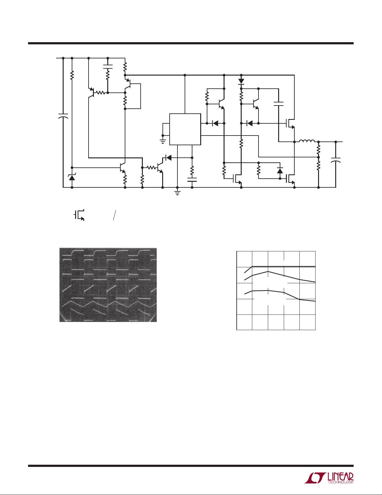
clock frequency. Figure 16 plots what is occurring, with
a pleasant surprise. As output current rises, loop oscillation frequency also rises until about 500Hz. At this point
the R6-C2 time constant fi lters the V
LT1070 transitions into “normal” operation. With the V
pin to DC and the
C
C
pin at DC it is convenient to think of A1 and the inverters as a linear error amplifi er with a closed-loop gain set
by the R1-R2 feedback divider. In fact, A1 is still duty
cycle modulating, but at a rate far above R6-C2’s break
frequency. The phase error contributed by C1 (which was
selected for low loop frequency at low output currents) is
dominated by the R6-C2 roll off and the R7-C3 lead into
A1. The loop is stable and responds linearly for all loads
beyond 80mA. In this high current region the LT1070 is
desirably “fooled” into behaving like Figure 11’s circuit.
A formal stability analysis for this circuit is quite complex,
but some simplifi cations lend insight into loop operation.
At 100μA loading (120kΩ) C1 and the load form a decay
time constant exceeding 300 seconds. This is orders of
magnitude larger than R7-C3, R6-C2, or the LT1070’s
40kHz commutation rate. As a result, C1 dominates the
loop. Wideband A1 sees phase shifted feedback, and very
1
low frequency oscillations similar to Figure 13’s occur
.
Although C1’s decay time constant is long, its charge
time constant is short because the circuit has low sourcing impedance. This accounts for the ramp nature of the
oscillations.
Increased loading reduces the C1 load decay time constant. Figure 16’s plot refl ects this. As loading increases,
the loop oscillates at a higher frequency due to C1’s decreased decay time. When the load impedance becomes
low enough C1’s decay time constant ceases to dominate
the loop. This point is almost entirely determined by R6
and C2. Once R6 and C2 “take over” as the dominant time
constant the loop begins to behave like a linear system.
In this region (e.g. above about 75mA, per Figure 16) the
LT1070 runs continuously at its 40kHz rate. Now, the R7C3 time constant becomes signifi cant, performing as a
2
simple feedback lead
to smooth output response. There is
A = 0.02V/DIV
(AC-COUPLED)
B = 5V/DIV
C = 2V/DIV
D = 10V/DIV
HORIZ = 20ms/DIV
AN29 F14
Figure 14. Low IQ Converter Waveforms at Light Loading
A = 0.02V/DIV
B = 5V/DIV
C = 2V/DIV
D = 10V/DIV
AN29 F15
2.5A
80
100
AN29 F16
Figure 15. Low I
550
500
450
400
350
300
250
IQ = 150μA
200
150
LOOP FREQUENCY (Hz)
100
50
0
0
HORIZ = 20μs/DIV
Converter Waveforms at 1 Amp Loading
Q
LINEAR REGION
EXTENDS TO
0.2Hz
20
OUTPUT (mA)
60
40
Figure 16. Figure 12’s Loop Frequency vs Output Current.
Note Linear Loop Operation Above 80mA
1
Some layouts may require substantial trace area to A1’s inputs. In such
cases the optional 10pF capacitor shown ensures clean transitions at A1’s
output.
2
“Zero Compensation” for all you technosnobs out there.
AN29-10
an32f
Page 11
A = 10V/DIV
B = 0.1V/DIV
(AC-COUPLED)
HORIZ = 5ms/DIV
Figure 17. Load Transient Response for Figure 12’s
Low IQ Regulator
AN29 F17
Application Note 29
3
constant decay
is visible as Trace B approaches steady state between the
4th and 5th vertical divisions.
A2 functions as a simple low-battery detector, pulling low
when V
drops below 4.8V.
IN
Figure 18 plots effi ciency versus output current. High
power effi ciency is similar to standard converters. Low
power effi ciency is somewhat better, although poor in
the lowest ranges. This is not particularly bothersome,
as power loss is very small.
(“rattling” is perhaps more appropriate)
100
90
80
70
60
50
40
EFFICIENCY (%)
30
20
10
0
0
Figure 18. Effi ciency vs Output Current for Figure 12.
Standby Effi ciency is Poor, But Power Loss Approaches
Battery Self Discharge
TYPICAL OPERATING
15mA
3mA
650μA
IQ = 150μA
0.5
1
OUTPUT CURRENT (A)
REGION
TYPICAL STANDBY
REGION
1.5
2
2.5
AN29 F18
a fundamental trade-off in the selection of the R7-C3 lead
network values. When the converter is running in its linear
region they must dominate the DC hysteresis deliberately
generated by R3-R4. As such, they have been chosen for
the best compromise between output ripple at high load
and loop transient response.
This loop provides a controlled, conditional instability
instead of the more usually desirable (and often elusive)
unconditional stability. This deliberately introduced characteristic lowers converter quiescent current by a factor of
60 without sacrifi cing high power performance. Although
demonstrated in a boost converter, it is readily exportable
to other confi gurations. Figure 19a’s step-down (buck
mode) confi guration uses the same basic loop with almost
no component changes. P-channel MOSFET Q1 is driven
from the LT1072 (a low power version of the LT1070) to
convert 12V to a 5V output. Q2 and Q3 provide current
limiting, while Q4 supplies turn off drive to Q1. the lower
output voltage mandates slightly different hysteresis biasing than Figure 12, accounting for the 1MΩ value at the
comparators positive input. In other respects the loop and
its performance are identical. Figure 19b uses the loop in
a transformer based multi-output converter. Note that the
fl oating secondaries allow a –12V output to be obtained
with a positive voltage regulator.
Low Quiescent Current Micropower 1.5V to 5V
Converter
Despite the complex dynamics transient response is quite
good. Figure 17 shows performance for a step from no
load to 1 ampere. When Trace A goes high a 1 ampere load
appears across the output (Trace B). Initially, the output
sags almost 150mV due to slow loop response time (the
R6-C2 pair delay V
pin response). When the LT1070 comes
C
on (signaled by the 40kHz “fuzz” at the bottom extreme
of Trace B) response is reasonably quick and surprisingly
well behaved considering circuit dynamics. The multi-time
Figure 20 extends our study of low quiescent current converters into the low voltage, micropower domain. In some
circumstances, due to space or reliability considerations, it
is preferable to operate circuitry from a single 1.5V cell. This
eliminates almost all ICs as design candidates. Although
it is possible to design circuitry which runs directly from
®
a single cell (see LTC
Application Note 15, “Circuitry For
Single Cell Operation”) a DC/DC converter permits using
higher voltage ICs. Figure 20’s design converts a single
3
Once again, “multi-pole settling” for those who adore jargon.
an32f
AN29-11
Page 12
Application Note 29
12V
(8V TO 16V)
IN
0.4Ω
1k100Ω
Q2
2N3906
Q1
IRF-9531
Q4
2N3904
L1
100μH
MUR405
5V
+
2700μF
1M
1M*
OUT
1500pF
100k
+
10μF
2k
1N4148
1N4148
1N4148
L1 = PULSE ENGINEERING, INC. # PE-92108
** = OPTIONAL. SEE TEXT
* = 1% FILM RESISTOR
Q3
2N3904
= 74C04
+
V
IN
V
LT1072
C
200Ω
47μF
V
GND
SW
FB NC
10k
12V
IN
–
1/2 LT1017
+
10pF**
UPDATE
Burst Mode regulators
can achieve lower I
Q
340k*
10k 470k
LT1004
1.2V
AN29 F19a
12V
IN
Figure 19a. The Low Quiescent Current Loop Applied to a Buck Converter
1.5V cell to a 5V output with only 125μA quiescent current.
Oscillator C1A’s output is a 2kHz square wave (Trace D,
Figure 21). The confi guration is conventional, except that
the biasing accommodates the narrow common mode
range dictated by the 1.5V supply. To maintain low power,
C1A’s integrating capacitor is small, with only 50mV of
swing. The parallel connected sides of C2 drive L1. When
the 5V output (Trace A) coasts down far enough C1B
goes low (Trace B), pulling both C2 positive inputs close
to ground. C1A’s clock now appears at the paralleled C2
outputs (Trace C), forcing energy into L1. The paralleled
outputs minimize saturation losses. L1’s fl yback pulses,
rectifi ed and stored in the 47μF capacitor, form the circuits
DC output. C1B on-off modulates C2 at whatever duty
cycle is required to maintain the circuits 5V output. The
LT1004 is the reference, with the resistor divider at C1B’s
positive input setting the output voltage. Schottky clamping
of C2’s outputs prevents negative going overdrives due to
parasitic L1 behavior.
AN29-12
an32f
Page 13
Application Note 29
12V
MUR120
L1
7
+
t
IN
22μF
+
4
t
2
2k
2W
0.2μF
3
8
9
MUR120
10
t
11
MBR360
5
+
+
t
L1
t
1
6
MUR120
V
GND
IN
LT1071
V
SW
V
C
+
FB NC
200Ω
C2
47μF
74C04 (5)
R6
470μF
470μF
C1
2700μF
LT1086
LT1086
1.2k
1.2k
11k
12V
IN
A1
1/2 LT1017
11k
–
+
+
10μF
12V
+
10μF
–12V
V
OUT
5V
1A
R3
R1
1M
1M*R710k
C3
0.005
R2
453k*
1N4148
L1 = PULSE ENGINEERING, INC. # PE-65108
* = 1% FILM RESISTOR
** = OPTIONAL. SEE TEXT
Figure 19b. Multi-Output, Transformer Coupled Low Quiescent Current Converter
The 1.2V LT1004 reference biasing is bootstrapped to the
5V output, permitting circuit operation down to 1.1V. A
10M bleed to supply ensures start-up. The 1M resistors
divide down the 1.2V reference, keeping C1B inside common mode limits. C1B’s positive feedback RC pair sets
about 100mV hysteresis and the 22pF unit suppresses
high frequency oscillation.
The micropower comparators and very low duty cycles at
light load minimize quiescent current. The 125μA fi gure
noted is quite close to the LT1017’s steady-state currents.
As load increases the duty cycle rises to meet the demand,
10pF**
R4
1N4148
10k
LT1004
1.2
AN29 F19b
R5
180k
12V
IN
requiring more battery power. Decrease in battery voltage
produces similar behavior. Figure 22 plots available output
current versus battery voltage. Predictably, the highest
power is available with a fresh cell (e.g., 1.5V to 1.6V),
although regulation is maintained down to 1.15V for 250μA
loading. The plot shows that the test circuit continued to
regulate below this point, but this cannot be relied on in
practice (LT1017 V
= 1.15V). The low supply voltage
MIN
makes saturation and other losses in this circuit diffi cult
to control. As such, effi ciency is about 50%.
an32f
AN29-13
Page 14
Application Note 29
3.9M
–
1.5M
150pF
3.9M
1.5V
470k
* = 1% METAL FILM RESISTOR
PNP = 2N3906
NPN = 2N3904
L1 = TRIAD # SP-29
C1A
1/2 LT1017
+
2M
240k
1.5V
150k
10M
–
C2B
1/2 LT1017
+
–
C2A
1/2 LT1017
+
V
IN
(1.1V TO 2V)
NC
1N4148
HP5082-2810
HP5082-2810
L1
5
6
HP-5082-2810
+
2.2μF
5V
OUT
22pF
1M*
0.001
+
C1B
1/2 LT1017
–
1M*
10M
360k
10M
V
IN
LT1004
1.2V
34
+
NC
2
1
4.3M*
47μF
619k*
390k
0.001
OPTIONAL FOR
NEGATIVE
OUTPUT
(SEE TEXT)
1.5V
C2B
C2A
Figure 20. 800μA Output 1.5V to 5V Converter
A = 100mV/DIV
(AC-COUPLED ON
LEVEL)
5V
DC
B = 2V/DIV
C = 2V/DIV
D = 2V/DIV
HORIZ = 5ms/DIV
AN29 F21
Figure 21. Waveforms for Low Power 1.5V to 5V Converter
5
6
TO 390kΩ
OF C2B
47μF
+
620k
14
3
850
800
750
= 5V
700
650
OUT
600
550
500
450
400
350
300
250
200
150
100
OUTPUT (μA) AVAILABLE AT V
22pF
1.2M* 10k5.1M
50
0
+
–
IQ = 125μA
0
1.05 1.15
C1B
V
OUT
EFFICIENCY ≈ 50%
GUARANTEED MINIMUM
OPERATING VOLTAGE
1.25
INPUT VOLTAGE (V)
10M 47k
= 5V
LT1017
1.35
LT1004
1.2V
1.45
V
1.55
AN29 F22
IN
Figure 22. Output Current Capability vs Input Voltage for Figure 20
AN29 F20
AN29-14
an32f
Page 15

Application Note 29
The optional connection in Figure 20 (shown in dashed
lines) takes advantage of the transformers fl oating secondary to furnish a –5V output. Drive circuitry is identical, but
C1B is rearranged as a current summing comparator. The
LT1004’s bootstrapped positive bias is supplied by L1’s
primary fl yback spikes.
200mA Output 1.5V to 5V Converter
Although useful, the preceding circuit is limited to low
power operation. Some 1.5V powered systems (survival
2-way radios, remote, transducer fed data acquisition
systems, etc.) require much more power. Figure 23’s
design supplies a 5V output with 200mA capacity. Some
sacrifi ce in quiescent current is made in this circuit. This is
predicated on the assumption that it operates continuously
22
+
1.5V
IN
L1
10k
–
1/2 LT1018
+
39k
47k
C1A
220μF
+
1N4148
1.5V
200k
1.5V
IN
10k
100Ω
HP5082-2810
1.5V
IN
Q1
2N2907
1k
2Ω
1/2 LT1018
1.5V
IN
V
+
IN
LT1070
V
C
1k
25μH
V
SW
FB
GND
6.8μF
0.01
68k
L1 = PULSE ENGINEERING, INC. # PE-92100
* = 1% METAL FILM RESISTOR
at high power. If lowest quiescent current is necessary the
technique detailed back in Figure 12 is applicable.
The circuit is essentially a fl yback regulator, similar to
Figure 11. The LT1070’s low saturation losses and ease
of use permit high power operation and design simplicity. Unfortunately, this device has a 3V minimum supply
requirement. Bootstrapping its supply pin from the 5V
output is possible, but requires some form of start-up
mechanism. Dual comparator C1 and the transistors form
a start-up loop. When power is applied C1A oscillates
(Trace A, Figure 24) at 5kHz. Q1 biases, driving Q2’s base
hard. Q2’s collector (Trace B) pumps L1, causing voltage
step-up fl yback events. These events are rectifi ed and
stored in the 500μF capacitor, producing the circuit’s DC
output. C1B is set up so it (Trace C) goes low when circuit
1N5823
5V
3.74k*
665Ω*
576Ω*
100k
47k
OUT
C1B “+”
1.5V
V
SUPPLY
INPUT
TO
IN
OPTIONAL IF
CAN EXCEED 1.7V
+V
1k
75k
LT1004
1.2V
100k
AN29 F23
UPDATE
LT1172 can be used
in place of LT1070
Q2
2N3507
C1B
+
500μF
–
+
Figure 23. 200mA Output 1.5V to 5V Converter
an32f
AN29-15
Page 16
Application Note 29
output crosses about 4.5V. When this occurs C1A’s integration capacitor is pulled low, stopping it from oscillating.
Under these conditions Q2 can no longer drive L1, but the
LT1070 can. This behavior is observable at the LT1070’s
pin (the junction of L1, Q2’s collector and the LT1070),
V
SW
Trace D. When the start-up circuit goes off, the LT1070 V
IN
pin has adequate supply voltage and it begins operation.
This occurs at the 4th vertical division of the photograph.
There is some overlap between start-up loop turn-off and
LT1070 turn-on, but it has no detrimental effect. Once the
circuit is running it functions similarly to Figure 11.
The start-up loop must be carefully designed to function
over a wide range of loads and battery voltages. Start-up
currents exceed 1 ampere, necessitating attention to Q2’s
saturation and drive characteristics. The worst case is a
nearly depleted battery and heavy output loading. Figure25
shows circuit output starting into a 100mA load at V
BATTERY
= 1.2V. The sequence is clean, and the LT1070 takes over at
the appropriate point. In Figure 26, loading is increased to
200mA. Start-up slope decreases, but starting still occurs.
The abrupt slope increase (6th vertical division) is due to
overlapping operation of the start-up loop and the LT1070.
Figure 27 plots input-output characteristics for the circuit.
Note that the circuit will start into all loads with V
BATTERY
=
1.2V. Start-up is possible down to 1.0V at reduced loads.
Once the circuit has started, the plot shows it will drive full
200mA loads down to V
possible down to V
BATTERY
BATTERY
= 1.0V. Reduced drive is
= 0.6V (a very dead battery)!
Figures 28 and 29, dynamic XY crossplot versions of
Figure 27, are taken at 20 and 200 milliamperes, respectively. Figure 30 graphs effi ciency at two supply voltages
over a range of output currents. Performance is attractive, although at lower currents circuit quiescent power
degrades effi ciency. Fixed junction saturation losses are
responsible for lower overall effi ciency at the lower supply
voltage. Figure 31 shows quiescent current increasing as
supply decays. Longer inductor current charge intervals
are necessary to compensate the decreased supply voltage.
A = 5V/DIV
B = 10V/DIV
C = 2V/DIV
D = 1V/DIV
(AC-COUPLED ON
5VDC LEVEL)
HORIZ = 2ms/DIV
AN29 F24
Figure 24. High Power 1.5V to 5V Converter Start-Up Sequence
VERT = 1V/DIV
HORIZ = 2ms/DIV
AN29 F25
Figure 25. High Power 1.5V to 5V Converter Turn-On Into a
100mA Load at V
BATT
= 1.2V
VERT = 1V/DIV
HORIZ = 2ms/DIV
AN29 F26
Figure 26. High Power 1.5V to 5V Converter Turn-On Into a
200mA Load at V
1.5
= 5V
1.4
OUT
1.3
1.2
1.1
1.0
0.9
0.8
0.7
0.6
0.5
0.4
0.3
0.2
0.1
0
MINIMUM INPUT VOLTAGE TO MAINTAIN V
0
= 1.2V
BATT
START
RUN
80
60 100 200
20 40
OUTPUT CURRENT (mA)
120 140
180160
AN29 F27
AN29-16
Figure 27. Input-Output Data for Figure 23
an32f
Page 17
VERT = OUTPUT
= 1V/DIV
HORIZ = INPUT = 0.15V/DIV
AN29 F28
Figure 28. Input-Output XY Characteristics of the
1.5V to 5V Converter at 20mA Loading
VERT = OUTPUT
= 1V/DIV
HORIZ = INPUT = 0.15V/DIV
AN29 F29
Figure 29. Input-Output XY Characteristics of the
1.5V to 5V Converter at 200mA Loading
HIGH EFFICIENCY CONVERTERS
High Effi ciency 12V to 5V Converter
Effi ciency is sometimes a prime concern in DC/DC converter design (see Appendix E, “Optimizing Converters
for Effi ciency”). In particular, small portable computers
frequently use a 12V primary supply which must be converted down to 5V. A 12V battery is attractive because it
offers long life when all trade-offs and sources of loss are
considered. Figure 32 achieves 90% effi ciency. This circuit
can be recognized as a positive buck converter. Transistor
Q1 serves as the pass element. The catch diode is replaced
with a synchronous rectifi er, Q2, for improved effi ciency.
The input supply is nominally 12V but can vary from 9.5V
to 14.5V. Power losses are minimized by utilizing low
source-to-drain resistance, 0.028Ω, NMOS transistors
for the catch diode and pass element. The inductor, Pulse
Engineering PE-92210K, is made from a low loss core
material which squeezes a little more effi ciency out of the
circuit. Also, keeping the current sense threshold voltage
low minimizes the power lost in the current limit circuit.
Application Note 29
100
V
= 5V
OUT
90
80
70
60
50
40
EFFICIENCY (%)
30
20
10
0
4020
0
Figure 30. Effi ciency vs Operating Point for Figure 23
1.50
1.45
1.40
1.35
1.30
1.25
1.20
1.15
SUPPLY VOLTAGE (V)
1.10
1.05
1.00
55
50
Figure 31. IQ vs Supply Voltage for Figure 23
Figure 33 shows the operating waveforms. Q5 drives the
synchronous rectifi er, Q2, when the V
turned “off”. Q2 is turned off through D1 and D2 when the
pin is “on”. To turn on Q1, the gate (Trace B) must
V
SW
be driven above the input voltage. This is accomplished
by bootstrapping the capacitor, C1, off the drain of Q2
(Trace C). C1 charges up through D1 when Q2 is turned on.
When Q2 is turned off, Q3 is able to conduct, providing a
path for C1 to turn Q1 on. During this time, current fl ows
through Q1 (Trace D) through the inductor (Trace E) and
into the load. To turn Q1 off, the V
Q5 is now able to turn on Q4 and the gate of Q1 is pulled
low through D3 and the 50Ω resistor. This resistor is used
to reduce the voltage noise generated by fast switching
characteristics of Q1. When Q2 is conducting (Trace F),
Q1 must be off. The effi ciency will be decreased if both
transistors are conducting at the same time. The 220Ω
VIN = 1.5V
VIN = 1.2V
120 140 180
8060
100
OUTPUT CURRENT (mA)
65 70
60
QUIESCENT CURRENT (mA)
SW
160
200
AN29 F30
80
75
AN29 F31
pin (Trace A) is
SW
pin must be “off”.
an32f
AN29-17
Page 18
Application Note 29
12V
(9.5V TO 14.5V)
IN
220μF
50k
Q8**
2N3906
100Ω
Q7**
2N3906
1k
+
LT1004-2.5
L1 = PULSE ENGINEERING, INC. # PE-92210K
* = 1% FILM RESISTORS
** = USE MATCHING OF 20mV AT 200μA
= P50N05E
(MOTOROLA)
0.018Ω47pF
R1
619Ω
Q6
2N2222
9k
IRFZ44
(INTERNATIONAL RECTIFIER)
100Ω
3.5k
1N4148
Q9
2N2222
E1
LT1072CN8
E2
GND
1N4148
5k
Q5
2N2222
D1
V
IN
V
1N4148
V
SW
FB
C
1μF
5k
Q3
2N2222C10.1μF
D3
1N4148
50Ω
220Ω1k
220Ω
Q4
VN2222
1N4148
D2
Q1
P50N05E
L1
100μH
Q2
P50N05E
3.01k*
1k*
AN29 F32
V
OUT
5V
5A
+
1000μF
Figure 32. 90% Effi ciency Positive Buck Converter with Synchronous Switch
A = 20V/DIV
B = 20V/DIV
C = 20V/DIV
D = 2A/DIV
E = 2A/DIV
F = 2A/DIV
HORIZ = 10μs/DIV
AN29 F33
Figure 33. Waveforms for 90% Effi ciency Buck Converter
resistors and D2 are used to minimize the overlap of the
switch cycles. Figure 34 shows the effi ciency versus load
plot for the circuit as shown. The other plots are for nonsynchronously switched buck regulators (see indicated
Figures).
Short circuit protection is provided by Q6 through Q9.
A 200μA current source is generated from an LT1004,
Q6 and the 9k resistor. This current fl ows through R1
and generates a threshold voltage of 124mV for the
comparator, Q7 and Q8. When the voltage drop across the
100
90
80
70
EFFICIENCY (%)
60
50
0
SYNC SWITCHES
PMOS AND DIODES
(SEE FIGURE 42)
PNP AND DIODES
(SEE FIGURE 42)
1
2
I
LOAD
(A)
3
4
5
AN29 F34
Figure 34. Effi ciency vs Load for Figure 32. The Synchronous
Switches Give Higher Effi ciency than Simple FET or Bipolar
Transistors and Diodes
0.018Ω sense resistor exceeds 124mV, Q8 is turned on.
The LT1072’s V
pin goes off when the VC pin is pulled
SW
below 0.9V. This occurs when Q8 forces Q9 to saturate.
An RC damper suppresses line transients that might
prematurely turn on Q8.
AN29-18
an32f
Page 19

Application Note 29
MBR1060
12V
IN
680Ω
V
IN
V
+
100μF
GND
L1 = PULSE ENGINEERING, INC. # PE-65066
* = 1% FILM RESISTORS
MBR1060 = MOTOROLA
LT1070
SW
FB
V
C
1k
1μF
MBR360
0.47μF
Figure 35. High Effi ciency Flux Sensed Isolated Converter
High Effi ciency, Flux Sensed Isolated Converter
Figure 35’s 75% effi ciency is not as good as the previous
circuit, but it has a fully fl oating output. This circuit uses
a bifi lar wound fl ux sensing secondary to provide isolated
voltage feedback. In operation the LT1070’s V
pin (Trace
SW
A, Figure 36) pulses L1’s primary, producing identical waveforms at the fl oating power and fl ux sensing secondaries
(Traces B and C). Feedback occurs from the fl ux sense
winding via the diode and capacitive fi lter. The 1k resistor provides a bleed current, while the 3.4k-1.07k divider
sets output voltage. The diode partially compensates the
diode in the power output winding, resulting in an overall
temperature coeffi cient of about 100ppm/°C. The oversize
diode aids effi ciency, although signifi cant improvement
(e.g., 5% to 10%) is possible if synchronous rectifi cation
is employed, as in Figure 32. The primary damper network
is unremarkable, although the 2k-0.1μF network has been
added to suppress excessive ringing at low output current.
2k
0.1μF
A = 10V/DIV
B = 10V/DIV
C = 10V/DIV
4
5
MBR1060
3
6
+
1000μF
+
22μF
HORIZ = 5μs/DIV
L1
t
8
t
t
1
5V
OUT
100mA TO 1A
(SEE TEXT)
3.40k*
1k
1.07k*
AN29 F35
AN29 F36
Figure 36. Waveforms for Flux Sensed Converter
This ringing is not deleterious to circuit operation, and the
network is optional. Below about 10% loading non-ideal
transformer behavior introduces signifi cant regulation error. Regulation stays within ±100mV from 10% to 100%
of output rating, with excursion exceeding 900mV at no
load. Figure 37’s circuit trades away isolation for tight
regulation with no output loading restrictions. Effi ciency
is the same.
an32f
AN29-19
Page 20
Application Note 29
12V
IN
680ΩL10.47μF
V
IN
V
+
100μF
GND
L1 = PULSE ENGINEERING, INC. # PE-65067
* = 1% FILM RESISTORS
Figure 37. Non-Isolated Version of Figure 35
LT1070
SW
V
C
1k
MBR360
FB
1μF
WIDE RANGE INPUT CONVERTERS
Wide Range Input –48V to 5V Converter
Often converters must accommodate a wide range of
inputs. Telephone lines can vary over considerable tolerances. Figure 38’s circuit uses an LT1072 to supply a 5V
output from a telecom input. The raw telecom supply is
nominally –48V but can vary from –40V to –60V. This range
of voltages is acceptable to the V
required for the V
pin (V
IN
MAX
Zener diode serve this purpose, dropping V
pin but protection is
SW
= 60V). Q1 and the 30V
’s voltage to
IN
acceptable levels under all line conditions.
Here the “top” of the inductor is at ground and the LT1072’s
ground pin at –V. The feedback pin senses with respect
to the ground pin, so a level shift is required from the 5V
output. Q2 serves this purpose, introducing only –2mV/°C
drift. This is normally not objectionable in a logic supply.
It can be compensated with the optional appropriately
scaled diode-resistor shown in Figure 38.
Frequency compensation uses an RC damper at the V
C
pin. The 68V Zener is a type designed to clamp and absorb
excessive line transients which might otherwise damage
the LT1072 (V
maximum voltage is 75V)
SW
MBR1060
8
4
t
1
+
1000μF
t
5
Figure 39 shows operating waveforms at the V
AN29 F37
5V
1A
3.01k*
1k*
OUT
SW
pin.
Trace A is the voltage and Trace B the current. Switching
is crisp, with well controlled waveforms. A higher current
version of this circuit appears in LTC Application Note 25,
“Switching Regulators For Poets.”
3.5V to 35V
IN
–5V
Converter
OUT
Figure 40’s approach has an even wider input range. In
this case it produces either a –5V or 5V output (shown in
dashed lines). This circuit is an extension of Figure 11’s
basic fl yback topology. The coupled inductor allows the
option for buck, boost, or buck-boost converters. This
circuit can operate down to 3.5V for battery applications
while accepting 35V inputs.
Figure 41 shows the operating waveforms for this circuit.
During the V
(Trace A) “on” time, current fl ows through
SW
the primary winding (Trace B). No current is transferred
to the secondary because the catch diode, D1, is reverse
biased. The energy is stored in the magnetic fi eld. When
the switch is turned “off” D1 forward biases and the energy
is transferred to the secondary winding. Trace C is the
voltage seen on the secondary and Trace D is the current
AN29-20
an32f
Page 21
INPUT
–48V
(–40V TO –60V)
3k
100μF
1/2W
220Ω
1N5936
30V
2.2μF
Q1
2N5550
+
68V**
+
V
IN
LT1072HV
GND
*
MUR410 (MOTOROLA)
**
1.5KE68A (MOTOROLA)
L1 = PULSE ENGINEERING, INC. # PE-92108
Figure 38. Wide Range Input Converter
Application Note 29
L1
1k
100μH
*
+
V
SW
FB
V
C
2k
0.22
330μF
2N5401
5V
OUT
0.5A
3.9k
1%
Q2
1.1k
1%
OPTIONAL
LOW DRIFT FEEDBACK
CONNECTION (SEE TEXT)
FROM
5V OUTPUT
3.01k
1%
Q2
2N5401
TO
FB PIN
TO
–48V
Q3
2N5401
1k
1%
3.01k
1%
AN29 F38
fl owing through it. This is not an ideal transformer so
not all of the primary windings energy is coupled into the
secondary. The energy left in the primary winding causes
the overvoltage spikes seen on the V
pin (Trace E). This
SW
phenomenon is modeled by a leakage inductance term
which is placed in series with the primary winding. When
the switch is turned “off” current continues to fl ow in the
inductor causing the snubber diode to conduct (Trace F).
The snubber diode current falls to zero as the inductor
loses its energy. The snubber network clamps the voltage
spike. When the snubber diode current reaches zero, the
pin voltage settles to a potential related to the turns
V
SW
ratio, output voltage and input voltage.
4
The feedback pin senses with respect to ground, so Q1
through Q3 provides the level shift from the –5V output.
Q1 introduces a –2mV/°C drift to the circuit. This effect can
be compensated by a circuit similar to the one shown in
Figure 38. Line regulation is degraded due to Q3’s output
impedance. If this is a problem, an op amp must be used
to perform the level shift (see AN19, Figure 29).
A = 50V/DIV
B = 0.5A/DIV
HORIZ = 5μs/DIV
AN29 F39
Figure 39. Waveforms for Wide Range Input Converter
Wide Range Input Positive Buck Converter
Figure 42 is another example of a positive buck converter.
This is a simpler version compared to the synchronous
switch buck, Figure 32. However, effi ciency isn’t as high
(see Figure 34). If the PMOS transistor is replaced with
a Darlington PNP transistor (shown in dashed lines)
effi ciency decreases further.
4
Application Note AN19, “LT1070 Design Manual,” page 25
an32f
AN29-21
Page 22

Application Note 29
VIN = 3.5V TO 35V
5V
V
IN
V
+
100μF
GND
L1 = PULSE ENGINEERING, INC. # PE-65050
* = 1% FILM RESISTORS
A = 20V/DIV
B = 4A/DIV
C = 10V/DIV
D = 4A/DIV
E = 20V/DIV
F = 2A/DIV
SW
LT1070
FB
V
C
1k 1k*
1μF
A, B, C, D HORIZ = 10μs/DIV
E, F HORIZ = 1μs/DIV
Figure 41. Waveforms for Wide Range Input Positive
–5V Output Flyback Converter
Figure 43a shows the operating waveforms for this circuit.
The pass transistor’s (Q1) drive scheme is similar to the one
shown in Figure 32. During the V
the gate of the pass transistor is pulled down through D1.
This forces Q1 to saturate. Trace B is the voltage seen on
the drain of Q1 and Trace C is the current passing through
Q1. The supply current fl ows through the inductor (Trace D)
and into the load. During this time energy is being stored
in the inductor. When voltage is applied to the inductor,
0.68μF
510Ω
1W
MBR360
(MOTOROLA)
n = 1
3
•
L1
4
2N3906
L1
Q3
1k*
1%
2
n = 1
•
1
MBR360
D1
Figure 40. Wide Range Input Positive-to-Negative Flyback Converter
AN29 F41
(Trace A) “on” time,
SW
1k*
1%
Q2
2N3906
Q1
1000μF
2N2222
3.32k*
1%
+
–5V
1A
OUT
V
IN
3
n = 1
4
V
SW
FB
MBR360
L1
2
+
•
1
OPTIONAL (SEE TEXT)
1000μF
5V
1A
3.01k*
1k*
OUT
AN29 F40
current does not instantly rise. As the magnetic fi eld builds
up, the current builds. This is seen in the inductor current
waveform (Trace D). When the V
pin is “off,” Q2 is able
SW
to conduct and turns Q1 off. Current can no longer fl ow
through Q1, instead D2 is conducting (Trace E). During
this period some of the energy stored in the inductor will
be transferred to the load. Current will be generated from
the inductor as long as there is any energy in it. This can
be seen in Figure 43a. This is known as continuous mode
operation. If the inductor is completely discharged, no
current will be generated (see Figure 43b). When this
happens neither switch, Q1 or D2, is conducting. The
inductor looks like a short and the voltage on the cathode
of D2 will settle to the output voltage. These “boingies”
can be seen in Trace B of Figure 43b. This is known as
discontinuous mode operation. Higher input voltages
can be handled with the gate-source Zener clamped by
D2. The 400 milliwatt Zener’s current must be rescaled
by adjusting the 50Ω value. Maximum gate-source voltage is 20V. The circuit will function up to 35V
. At inputs
IN
beyond 35V all semiconductor breakdown voltages must
be considered.
AN29-22
an32f
Page 23

Application Note 29
V
12V TO 35V
100μF
2N3906
5.1k
0.1Ω
1k
1k
V
IN
E1
E2
GND
100pF
IN
+
L1 = PULSE ENGINEERING, INC # PE-92113
* = 1% FILM RESISTORS
LT1072CN8
1N4148
2N2222
V
SW
V
1k
1N4148
51Ω
1W
FB
C
1k
1μF
Q2
2N2222A
D1
OPTIONAL
(SEE TEXT)
1k
IRF9Z30
(HEAT SINK)
D2
12V
1N759
(OPT)
(HEAT SINK)
2N2222
Q1
2N6667
L1
170μH
D2
MBR735
(MOTOROLA)
100μF
+
AN29 F42
5V
5A
3.01k*
1k*
OUT
Figure 42. Positive Buck Converter
A = 10V/DIV
B = 10V/DIV
C = 2A/DIV
D = 2A/DIV
E = 2A/DIV
HORIZ = 10μs/DIV
AN29 F43a
Figure 43a. Waveforms for Wide Range Input Positive Buck
Converter (Continuous Mode)
1N4148
100Ω
1W
A = 10V/DIV
B = 10V/DIV
C = 0.5A/DIV
D = 0.5A/DIV
E = 0.5A/DIV
HORIZ = 10μs/DIV
AN29 F43b
Figure 43b. Waveforms for Wide Range Input Positive Buck
Converter (Discontinuous Mode)
an32f
AN29-23
Page 24
Application Note 29
28V NOMINAL
(15V TO 35V)
100μF
1k
Q2
2N2222A
1N4148
220Ω
+
V
IN
E1
LT1072CN8
E2
GND
L1 = PULSE ENGINEERING, INC # PE-52627
* = 1% FILM RESISTORS
1W
D1
1N4148
V
SW
FB
V
C
1k
1μF
Figure 44. Positive Buck-Boost Converter
IRF9Z30
7.5V
1N755
D2
MBR360
Q1
L1
330μH
D3
MBR360
(MOTOROLA)
D4
MBR360
28V
+
1000μF
250mA
26.1k
1.21k*
AN29 F44
Buck-Boost Converter
The buck boost topology is useful when the input voltage can either be higher or lower than the output. In this
example, Figure 44, this is accomplished with a single
inductor instead of a transformer, as in Figure 40 (optional).
However, the input voltage range only extends down to
15V and can reach to 35V. If the maximum 1.25A switch
current rating of the LT1072 is exceeded an LT1071 or
LT1070 can be used instead. At high power levels package
thermal characteristics should be considered.
The operation of the circuit is similar to the positive buck
converter, Figure 42. The gate drive to the pass transistor
is derived the same way except the gate-source voltage is
clamped. Remember, the gate-source maximum voltage
rating is specifi ed at ±20V. Figure 45 shows the operating
waveforms. When the V
pin is “on” (Trace A), the pass
SW
transistor, Q1, is saturated. The gate voltage (Trace B) is
clamped by the Zener diode. Trace C is the voltage on the
drain of Q1 and Trace D is the current through it. This
is where the similarities between the two circuits end.
Notice the inductor is pulled to within a diode drop, D2
above ground, instead of being tied to the output (see
A = 20V/DIV
B = 10V/DIV
C = 20V/DIV
D = 2A/DIV
E = 2A/DIV
F = 2A/DIV
HORIZ = 10μs/DIV
AN29 F45
Figure 45. Waveforms for Positive Buck-Boost Converter
Figure 42). In this case, the inductor has the input voltage
applied across it, except for a Vbe and saturation losses.
D4 is reverse biased and blocks the output capacitor from
discharging into the V
pin. When the VSW pin is “off” Q1
SW
and D2 cease to conduct. Since the current in the inductor
(Trace E) continues to fl ow, D3 and D4 are forward biased
and the energy in the inductor is transferred into the load.
Trace F is the current through D3. Also, D2 keeps Q1 from
staying on if the circuit is operating in buck mode. D1, on
the other hand, blocks current from fl owing into the gate
drive circuit when operating in boost mode.
AN29-24
an32f
Page 25

INPUT
10k
Q1
2N6667
335μH
MR1122
Application Note 29
V
≈ 1.8V
L1
+
10,000μF
470
REF
LT1083
IN OUT
ADJ
240*
OUTPUT
+
10μF
1k
0.001
1M
LT1011
4
1
28V
4N28
+
10k
10k
–
1N914
Figure 46. High Power Linear Regulator with Switching Pre-Regulator
A = 200mV/DIV
(AC-COUPLED)
B = 50V/DIV
C = 20V/DIV
D = 5A/DIV
HORIZ = 500μs/DIV
AN29 F47
Figure 47. Switching Pre-Regulated Linear Regulators Waveforms
Wide Range Switching Pre-Regulated Linear
Regulator
In a sense, linear regulators can be considered extraordinarily wide range DC/DC converters. They do not face
the dynamic problems switching regulators encounter
under varying ranges of input and output. Excess energy
is simply dissipated at heat. This elegantly simplistic
energy management mechanism pays dearly in terms of
effi ciency and temperature rise. Figure 46 shows a way a
linear regulator can more effi ciently control high power
under widely varying input and output conditions.
The regulator is placed within a switched-mode loop that
servo-controls the voltage across the regulator. In this
arrangement the regulator functions normally while the
switched-mode control loop maintains the voltage across it
1N914
28V
V
≈ 1.8V
REF
L1 = PULSE ENGINEERING, INC. # PE-51518
* = 1% FILM RESISTOR
2k
AN29 F46
at a minimal value, regardless of line, load or output setting
changes. Although this approach is not quite as effi cient as
a classical switching regulator, it offers lower noise and the
fast transient response of the linear regulator. The LT1083
functions in the conventional fashion, supplying a regulated
output at 7.5A capacity. The remaining components form
the switched-mode dissipation limiting control. This loop
forces the potential across the LT1083 to equal the 1.8V
value of V
. The opto-isolator furnishes a convenient
REF
way to single end the differentially sensed voltage across
the LT1083. When the input of the regulator (Trace A,
Figure 47) decays far enough, the LT1011 output (Trace B)
switches low, turning on Q1 (Q1 collector is Trace C). This
allows current fl ow (Trace D) from the circuit input into the
10,000μF capacitor, raising the regulator’s input voltage.
When the regulator input rises far enough, the comparator
goes high, Q1 cuts off and the capacitor ceases charging. The MR1122 damps the fl yback spike of the current
limiting inductor. The 0.001μF-1M combination sets loop
hysteresis at about 100mV
. This free-running oscil-
P-P
lation control mode substantially reduces dissipation in
the regulator, while preserving its performance. Despite
changes in the input voltage, different regulated outputs or
load shifts, the loop always ensures minimum dissipation
in the regulator.
an32f
AN29-25
Page 26

Application Note 29
100
90
P
= 12W
OUT
80
70
P
= 15W
OUT
P
= 5W
60
OUT
50
40
P
= 5W
OUT
EFFICIENCY (%)
30
20
10
0
0
V
= 5V VIN = 15V
OUT
V
= 5V VIN = 28V
OUT
1
V
OUT
V
OUT
VIN = 15V
= 12V
VIN = 28V
= 15V
LT1083 WITH NO PRE-REGULATOR. THEORETICAL LIMITS ONLY.
DISSIPATION LIMITED
LT1083 WITH NO PRE-REGULATOR. THEORETICAL LIMITS ONLY.
DISSIPATION LIMITED
2
3
OUTPUT (A)
Figure 48. Effi ciency vs Output Current for Figure 46 at Various Operating Points
Figure 48 plots effi ciency at various operating points. Junction losses and the loop enforced 1.8V across the LT1083
are relatively small at high output voltages, resulting in
good effi ciency. Low output voltages do not fare as well,
but compare very favorably to the theoretical data for the
LT1083 with no pre-regulator. At the higher theoretical
dissipation levels the LT1083 will shut down, precluding
practical operation.
HIGH VOLTAGE CONVERTERS
High Voltage Converter—1000V
, Nonisolated
OUT
Photomultiplier tubes, ion generators, gas-based detectors, image intensifi ers and other applications need high
voltages. Converters frequently supply these potentials.
Generally, the limitation on high voltage is transformer
insulation breakdown. A transformer is almost always
used because a simple inductor forces excessive voltages on the semiconductor switch. Figure 49’s circuit,
reminiscent of Figure 11’s basic fl yback confi guration, is
a 15V to 1000V
converter. The LT1072 controls out-
OUT
put by modulating the fl yback energy into L1, forcing its
feedback (FB) pin to 1.23V (the internal reference value).
In this example loop compensation is heavily overdamped
by the V
spikes within the V
Fully Floating, 1000V
pin capacitor. L1’s damper network limits fl yback
C
pin’s 75V rating.
SW
Converter
OUT
Figure 50 is similar to Figure 49 but features a fully fl oating
output. This provision allows the output to be referenced
off system ground, often desirable for noise or biasing
reasons. Basic loop action is as before, except that the
P
= 85W
OUT
P
= 105W
OUT
P
= 35W
OUT
P
OUT
6
15V
22μF
+
L1
3
1k
1/2W
1
MUR120
V
IN
SW
FB
LT1072
V
C
= SEMTEC, FM-50
= 35W
2μF
7
8
7
AN29 F48
0.1μF
2000V
*
V
1000V
5W
10M
1%
(SEE NOTES)
12.4k 1%
(IDEAL VALUE–PAD AS REQUIRED
FOR 1000V
OUT
OUT
)
4
= 5V
= 5V
VIN = 15V
VIN = 28V
5
0.47
15V
V
GND
L1 = PULSE ENGINEERING, INC. # PE-6197
10M = MAX-750-22 VICTOREEN, INC.
*
V
OUT
V
OUT
Figure 49. Nonisolated 15V to 1000V Converter
LT1072’s internal error amplifi er and reference are replaced
with galvanically isolated equivalents. Power for these
components is bootstrapped from the output via source
follower Q1 and its 2.2M ballast resistor. A1 and the LT1004,
micropower components, minimize dissipation in Q1 and
its ballast. Q1’s gate bias, tapped from the output divider
string, produces about 15V at its source. A1 compares the
scaled divider output with the LT1004 reference. The error
signal, A1’s output, drives the opto-coupler. Photocurrent
is kept low to save power. The opto-coupler output pulls
down on the V
tion at the V
pin, closing a loop. Frequency compensa-
C
pin and A1 stabilizes the loop.
C
an32f
AN29-26
Page 27

15V
Application Note 29
1000V
IN
1k
MUR120
V
IN
FBNC
V
* = 1% METAL FILM RESISTOR
10M = VICTOREEN MAX-750-22
L1 = PULSE ENGINEERING, INC. # PE-6197
L1
3
0.47
1
V
SW
LT1072
GND
C
1k
2μF
= INPUT GROUND
= OUTPUT COMMON
= SEMTEC, FM-50
7
8
3.6k
4N46
0.1μF
2000V
180k
8
LT1006
1M
0.68
2.2M
0.1
D
Q1
VN2222
S
7
200k
+
A1
10k
–
4
LT1004
1.2V
OUT
5W
10M (SEE NOTES)
1%
200k*
5k
OUTPUT
ADJUST
10k*
AN29 F50
Figure 50. Isolated Output 15V to 1000V Converter
The transformers isolated secondary and optical feedback
produce a regulated, fully galvanically fl oating output.
Common mode voltages of 2000V are acceptable.
20,000V
Breakdown Converter
CMV
Figure 50’s common mode breakdown limits are imposed
by transformer and opto-coupler restrictions. Isolation
amplifi ers, transducer measurement at high common mode
voltages (e.g., winding temperature of a utility company
transformer and ESD sensitive applications) require high
breakdowns. Additionally, very precise fl oating measurements, such as signal conditioning for high impedance
bridges, can require extremely low leakage to ground.
Achieving high common mode voltage capability with
minimal leakage requires a different approach. Magnetics is usually considered the only approach for isolated
transfer of appreciable amounts of electrical energy.
Transformer action is, however, achievable in the acoustic
domain. Some ceramic materials will transfer electrical
energy with galvanic isolation. Conventional magnetic
transformers work on an electrical-magnetic-electrical
basis using the magnetic domain for electrical isolation.
The acoustic transformer uses an acoustic path to get
isolation. The high voltage breakdown and low electrical
conductance associated with ceramics surpasses isolation
characteristics of magnetic approaches. Additionally, the
acoustic transformer is simple. A pair of leads bonded to
each end of the ceramic material forms the device. Insula-
12
tion resistance exceeds 10
Ω, with primary-secondary
capacitances of 1pF to 2pF. The material and its physical
confi guration determine its resonant frequency. The device
may be considered as a high Q resonator, similar to a quartz
crystal. As such, drive circuitry excites the device in the
positive feedback path of a wideband gain element. Unlike
a crystal, drive circuitry is arranged to pass substantial
current through the ceramic, maximizing power into the
transformer.
an32f
AN29-27
Page 28
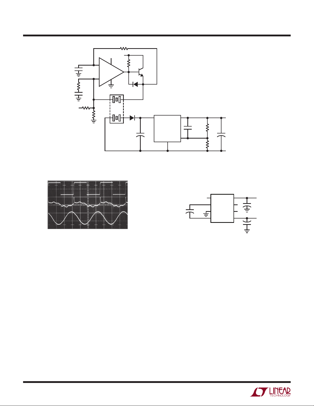
Application Note 29
15V
–
15V
0.002
100Ω
470pF
1k
LT1011
+
680Ω
SECONDARY
Figure 51. 15V to 10V Converter with 20,000V Isolation
15V
PRIMARY
2k
2k
1N4148
PIEZOCERAMIC
TRANSFORMER
1N4148
+
Q1
2N3904
10μF
* = 1% METAL FILM RESISTOR
PIEZOCERAMIC TRANSFORMERS
AVAILABLE FROM CHANNEL
INDUSTRIES, INC. SANTA BARBARA, CA.
V
IN
LT1020
GND
23
V
OUT
0.001μF
11
FB
1.5M*
500k*
+
AN29 F51
10V
FLOATING
OUTPUT
100μF
FLOATING
OUTPUT
COMMON
A = 10V/DIV
V
C2
+
AN29 F53
IN
2μF
–V
100μF
B = 20mA/DIV
C = 20V/DIV
HORIZ = 2μs/DIV
AN29 F52
1
+
C1
10μF
2
3
4
LT1054
8
+
7
6
5
Figure 52. Waveforms for the 20,000V Isolation Converter Figure 53. A Basic Switched-Capacitor Converter
In Figure 51, the piezo-ceramic transformer is in the LT1011
comparators positive feedback loop. Q1 is an active pull-up
for the LT1011, an open-collector device. The 2k-0.002μF
path biases the negative input. Positive feedback occurs at
the transformers resonance, and oscillation commences
(Trace A, Figure 52 is Q1’s emitter). Similar to quartz
crystals, the transformer has signifi cant harmonic and
overtone modes. The 100Ω-470pF damper suppresses
transitions. The transformer looks like a highly resonant
fi lter to the resultant acoustic wave propagated in it. The
secondary voltage (Trace C) is sinusoidal. Additionally, the
transformer has voltage gain. The diode and 10μF capacitor convert the secondary voltage to DC. The LT1020 low
quiescent current regulator gives a stabilized 10V output.
Output current for the circuit is a few milliamperes. Higher
currents are possible with attention to transformer design.
spurious oscillations and “mode hopping.” Drive current
(Trace B) approximates a sine wave, with peaking at the
OUT
AN29-28
an32f
Page 29

Application Note 29
2
3.5V ≤ VIN ≤ 15V
= C
C
1
VOLTAGE LOSS (V)
0
0
Figure 54. Losses for the Basic Switched-Capacitor Converter Figure 55. Switched-Capacitor –VIN to +V
+
= 100μF
IN
OUT
TJ = 125°C
•
INDICATES GUARANTEED TEST POINT
•
2010
OUTPUT CURRENT (mA)
1
2
10μF
3
4
4030
LT1054
TJ = 25°C
60 70 90
50
V
8
7
6
5
IN
TJ = –55°C
80
≥ 6V
100μF
+
AN29 F54
10k
0.002
100
•
1
2
3
4
0.001μF
+
AN29 F56
1N4001
LT1054
10μF
5V
100mA
–5V
75mA
9
GND
8
–IN
5
COMP
PNP
+IN
7
0.001μF
1M* 499k* 100k
VN2222
3
V
IN
LT1020
REF
OUT
+V
OUT
–V
COMP
NPN
1N4001
+
IN
OUT
FB
64
2
11
100μF
500k*
500k*
+
10μF
2μF
+
+
10μF
AN29 F55
OUT
OUT
OUT
8
7
6
5
Converter
100k
Figure 56. High Current Switched-Capacitor 6V to ±5V Converter
SWITCHED-CAPACITOR BASED CONVERTERS
Inductors are used in converters because they can store
energy. This stored magnetic energy, released and expressed in electrical terms, is the basis of converter operation. Inductors are not the only way to store energy with
effi cient release expressed in electrical terms. Capacitors
store charge (already an electrical quantity) and as such,
can be used as the basis for DC/DC conversion. Figure 53
shows how simple a switched-capacitor based converter
can be (the fundamentals of switched-capacitor based
conversion are presented in Appendix B, “Switched-Capacitor Voltage Converters—How They Work”). The LT1054
provides clocked drive to charge C1. A second clock phase
discharges C1 into C2. The internal switching is arranged
so C1 is “fl ipped” during the discharge interval, producing a negative output at C2. Continuous clocking allows
C2 to charge to the same absolute value as C1. Junction
and other losses preclude ideal results, but performance
is quite good. This circuit will convert V
to –V
IN
OUT
with
losses shown in Figure 54. Adding an external resistive
divider allows regulated output (see Appendix B).
With some additional steering diodes this confi guration
can effectively run “backwards” (Figure 55), converting
a negative input to a positive output. Figure 56’s variant
gives low dropout linear regulation for 5V and –5V outputs from 6V
. The LT1020-based dual output regulation
IN
an32f
AN29-29
Page 30

Application Note 29
V
scheme is adapted from Figure 8. Figure 57 uses diode
steering to get voltage boost, providing ≈2V
. Bootstrap-
IN
ping this confi guration with Figure 54’s basic circuit leads
to Figure 58, which converts a 5V input to 12V and –12V
outputs. As might be expected output current capacity is
traded for the voltage gain, although 25mA is still available.
Figure 59, another boost converter, employs a dedicated
version of Figure 58 (the LT1026) to get regulated ±7V
from a 6V input. The LT1026 generates unregulated ±11V
rails from the 6V input with the LT1020 and associated
components (again, purloined from Figure 8) producing
regulation. Current and boost capacity are reduced from
Figure 58’s levels, but the regulation and simplicity are
noteworthy. Figure 60 combines the LT1054’s clocked
switched-capacitor charging with classical diode voltage
multiplication, producing positive and negative outputs.
At no load ±13V is available, falling to ±10V with each
side supplying 10mA.
V
IN
3.5V TO 15V
1N4001
+
V
OUT
+
+
100μF
–
= 3.5V TO 15V
V
IN
≈ 2VIN – (VL + 2V
V
OUT
= LT1054 VOLTAGE LOSS
V
L
DIODE
)
Figure 57. Voltage Boost Switched-Capacitor Converter
10μF
1
2
3
4
1N4001
LT1054
+
2μF
8
7
6
5
AN29 F57
High Power Switched-Capacitor Converter
Figure 61 shows a high power switched-capacitor converter
with a 1A output capacity. Discrete devices permit high
power operation.
The LTC1043 switched-capacitor building block provides
non-overlapping complementary drive to the Q1-Q4 power
MOSFETs. The MOSFETs are arranged so that C1 and
C2 are alternately placed in series and then in parallel.
During the series phase, the 12V supply current fl ows
through both capacitors, charging them and furnishing
load current. During the parallel phase, both capacitors
deliver current to the load. Traces A and B, Figure 62, are
the LTC1043-supplied drives to Q3 and Q4, respectively.
Q1 and Q2 receive similar drive from Pins 3 and 11. The
diode-resistor networks provide additional non-overlapping drive characteristics, preventing simultaneous drive
to the series-parallel phase switches. Normally, the output
would be one-half of the supply voltage, but C1 and its
associated components close a feedback loop, forcing
the output to 5V. With the circuit in the series phase, the
output (Trace C) heads rapidly positive. When the output
exceeds 5V, C1 trips, forcing the LTC1043 oscillator pin
(Trace D) high. This truncates the LTC1043’s triangle wave
oscillator cycle. The circuit is forced into the parallel phase
and the output coasts down slowly until the next LTC1043
clock cycle begins. C1’s output diode prevents the triangle
down-slope from being affected and the 100pF capacitor
provides sharp transitions. The loop regulates the output to
AN29-30
V
= 5V
IN
+
5μF
V
≈ 12V
OUT
= 25mA
I
100μF
OUT
2N2219
+
1k
1
+
2
10μF
3
4
LT1054
#1
8
7
6
5
1N914
+
100μF
5μF
+
1N914
+
10μF
1
+
2
10μF
3
4
LT1054
#2
8
20k
7
6
5
1N5817
100μF
+
AN29 F58
V
I
OUT
OUT
≈ –12
= 25mA
Figure 58. Switched-Capacitor 5V to ±12V Converter
an32f
Page 31

Application Note 29
5V by feedback controlling the turn-off point of the series
phase. The circuit constitutes a large scale switched-capacitor voltage divider which is never allowed to complete
a full cycle. The high transient currents are easily handled
by the power MOSFETs and overall effi ciency is 83%.
REFERENCES
Williams, J., “Conversion Techniques Adopt Voltages to
your Needs,” EDN, November 10, 1982, p. 155.
Williams, J., “Design DC/DC Converters to Catch Noise
at the Source,” Electronic Design, October 15, 1981, p.
229.
Nelson, C., “LT1070 Design Manual,” Linear Technology
Corporation, Application Note 19.
Williams, J., “Switching Regulators for Poets,” Linear
Technology Corporation, Application Note 25.
1μF
+
1
+
2
1μF
1μF
+
LT1026
3
4
8
+
7
6
6V
IN
5
100k
1μF
0.002μF
≈11V NO LOAD
8
–IN
5
COMP
PNP
0.001μF
1M* 360k* 100k
VN2222 *1% METAL FILM RESISTOR
Williams, J., “Power Conditioning Techniques for Batteries,” Linear Technology Corporation, Application Note 8.
Tektronix, Inc., CRT Circuit, Type 453 Operating Manual,
p. 3-16.
Pressman, A. I., “Switching and Linear Power Supply,
Power Converter Design,” Hayden Book Co., Hasbrouck
Heights, New Jersey, 1977, ISBN 0-8104-5847-0.
Chryssis, G., “High Frequency Switching Power Supplies,
Theory and Design,” McGraw Hill, New York, 1984, ISBN
0-07-010949-4.
Sheehan, D., “Determine Noise of DC/DC Converters,”
Electronic Design, September 27, 1973.
Bright, Pittman, and Royer, “Transistors as On-Off Switches
in Saturable Core Circuits,” Electronic Manufacturing,
October, 1954.
9
3
GND
V
+IN
IN
LT1020
COMP
REF
NPN
OUT
7
2
OUT
500k*
11
FB
270k*
64
0.001μF
7V
OUT
20mA
+
100μF
+
10μF
–7V
OUT
AN29 F59
20mA
≈–11V NO LOAD
100k
Figure 59. Switched-Capacitor Based 6V to ±7V Converter
= 1N4148
1
2
LT1054
3
4
10μF
+
+V
OUT
+
100μF
+
10μF
10μF
+
+
C1
10μF
8
5V
7
6
5
10μF 10μF
+
+
+
10μF
+
10μF
+
100μF
–V
OUT
AN29 F60
Figure 60. Switched-Capacitor Charge Pump Based Voltage Multiplier
an32f
AN29-31
Page 32

Application Note 29
12V
12V
IN
180pF
12k
12V
IN
–
+
22k
LT1004
1.2V REFERENCE
V
OUT
5V
1A
12V
IN
2k
6
LTC1043
7
13
6
18
8
11
12
14
5
2
3
15
17
416
1k
12V
1k
12V
12V
IN
S
Q1
D
470μF
D
Q4
S
ALL DIODES ARE 1N4148
Q1, Q2, Q3 = IRF9531 P-CHANNEL
Q4 = IRF533 N-CHANNEL
SQ3D
1k
SQ2D
1k
AN29 F61
+
8
C1
LT1011
1
4
100pF
470μF 38k
Figure 61. High Power Switched-Capacitor Converter
A = 20V/DIV
B = 20V/DIV
C = 0.1V/DIV
(AC-COUPLED)
D = 10V/DIV
HORIZ = 20μs/DIV
AN29 F62
Figure 62. Waveforms for Figure 61
an32f
AN29-32
Page 33

Application Note 29
APPENDIX A
The 5V to ±15V Converter—A Special Case
Five volt logic supplies have been standard since the introduction of DTL logic over twenty years ago. Preceding and
during DTL’s infancy the modular amplifi er houses standardized on ±15V rails. As such, popular early monolithic
amplifi ers also ran from ±15V rails (additional historical
perspective on amplifi er power supplies appears in AN11’s
appended section, “Linear Power Supplies—Past, Present
and Future”). The 5V supply offered process, speed and
density advantages to digital ICs. The ±15V rails provided
a wide signal processing range to the analog components.
These disparate needs defi ned power supply requirements
for mixed analog-digital systems at 5V and ±15V. In systems with large analog component populations the ±15V
supply was and still is usually derived from the AC line.
Such line derived ±15V power becomes distinctly undesirable in predominantly digital systems. The inconvenience,
diffi culty and cost of distributing analog rails in heavily
digital systems makes local generation attractive. 5V to
±15V DC/DC converters were developed to fi ll this need
and have been with us for about as long as 5V logic.
Figure A1 is a conceptual schematic of a typical converter.
The 5V input is applied to a self-oscillating confi guration
composed of transistors, a transformer and a biasing
network. The transistors conduct out of phase, switching
(Figure A2, Traces A and C are Q1’s collector and base,
while Traces B and D are Q2’s collector and base) each
5
time the transformer saturates.
Transformer saturation
causes a quickly rising, high current to fl ow (Trace E).
This current spike, picked up by the base drive winding,
switches the transistors. Transformer current abruptly
drops and then slowly rises until saturation again forces
switching. This alternating operation sets transistor duty
cycle at 50%. The transformers secondary is rectifi ed,
fi ltered and regulated to produce the output.
This confi guration has a number of desirable features. The
complementary high frequency (typically 20kHz) square
wave drive makes effi cient use of the transformer and allows
relatively small fi lter capacitors. The self-oscillating primar y
drive tends to collapse under overload, providing desirable short-circuit characteristics. The transistors switch
in saturated mode, aiding effi ciency. This hard switching,
combined with the transformer’s deliberate saturation does,
however, have a drawback. During the saturation interval
a signifi cant, high frequency current spike is generated
5
This type of converter was originally described by Royer, et al. See
References.
5V
IN
INPUT
FILTER
4
Q1
Q2
R1
BASE BIASING
AND DRIVE
Figure A1. Conceptual Schematic of a Typical 5V to ±15V Converter
C1
SWITCHING
R2
POWER
5
6
1
2
3
OUTPUT
+
REGULATORS
+
LINEAR
+V
–V
REG
COMMON
REG
AN29 FA1
15V
OUT
–15V
an32f
AN29-33
Page 34
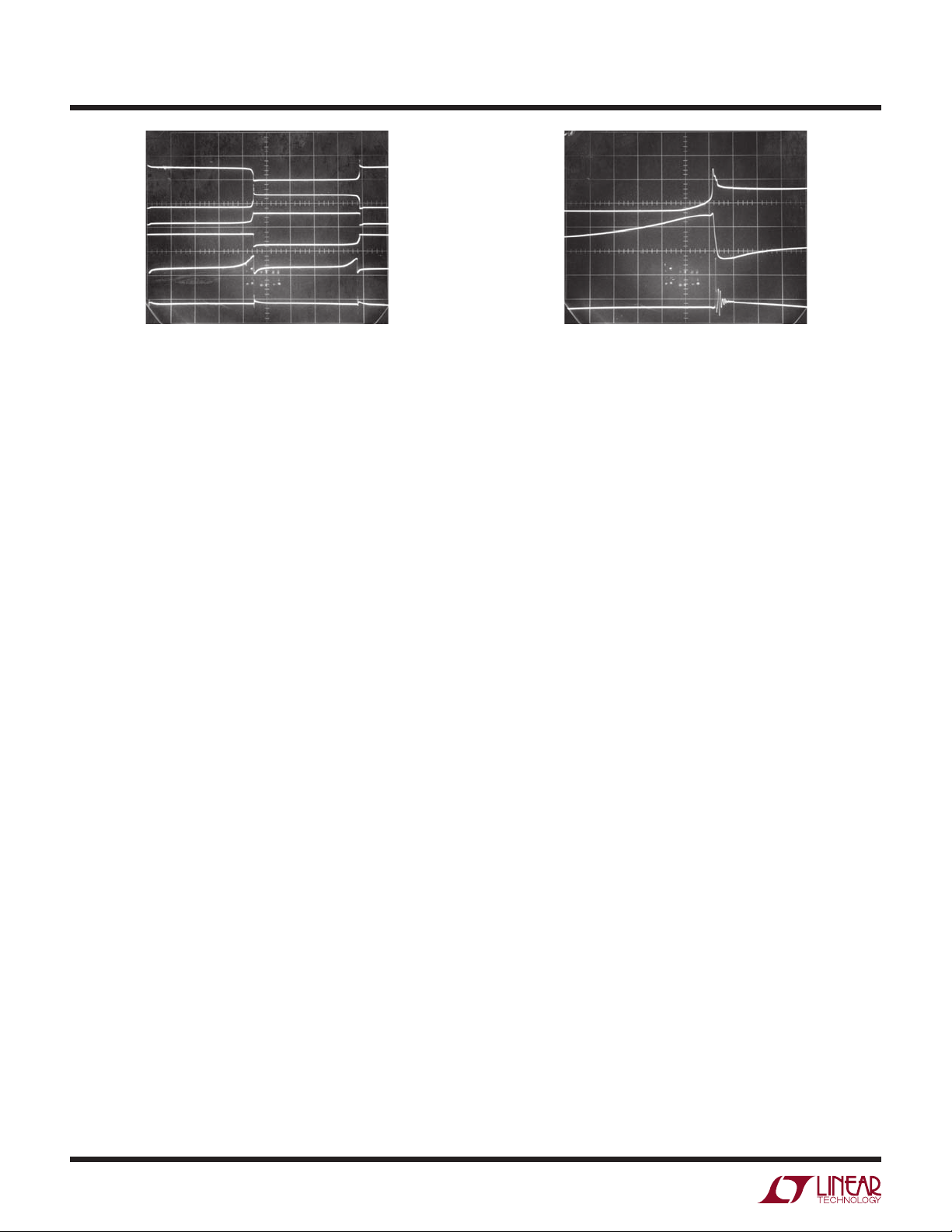
Application Note 29
A = 20V/DIV
B = 20V/DIV
C = 2V/DIV
D = 2V/DIV
E = 5A/DIV
A = 10V/DIV
B = 2A/DIV
F = 0.02V/DIV
HORIZ = 5μs/DIV
Figure A2. Typical 5V to ±15V Saturating Converters Waveforms Figure A3. Switching Details of Saturating Converter
AN29 FA2
(again, Trace E). This spike causes noise to appear at the
converter outputs (Trace F is the AC-coupled 15V output).
Additionally, it pulls signifi cant current from the 5V supply.
The converters input fi lter partially smooths the transient,
but the 5V supply is usually so noisy the disturbance is
acceptable. The spike at the output, typically 20mV high, is
a more serious problem. Figure A3 is a time and amplitude
expansion of Figure A2’s Traces B, E and F. It clearly shows
C = 10mV/DIV
HORIZ = 500ns/DIV
AN29 FA3
drive, ensuring transistor saturation under heavy loading
but wasting power at lighter loads. Adaptive bias schemes
will mitigate this problem, but increase complexity and
almost never appear in converters of this type.
The noise problem is, however, the main drawback of this
approach to 5V to ±15V conversion. Careful design, layout,
fi ltering and shielding (for radiated noise) can reduce noise,
but cannot eliminate it.
the relationship between transformer current (Trace B,
Figure A3), transistor collector voltage (Trace A, Figure A3)
and the output spike (Trace C, Figure A3). As transformer
current rises, the transistor starts coming out of saturation. When current rises high enough the circuit switches,
causing the characteristic noise spike. This condition is
exacerbated by the other transistors concurrent switching,
causing both ends of the transformer to simultaneously
conduct current to ground.
Some techniques can help these converters with the noise
problem. Figure A4 uses a “bracket pulse” to warn the
powered system when a noise pulse is about to occur.
Ostensibly, noise sensitive operations are not carried
out during the bracket pulse interval. The bracket pulse
(Trace A, Figure A5) drives a delayed pulse generator
which triggers (Trace B) the fl ip-fl op. The fl ip-fl op output
biases the switching transistors (Q1 collector is Trace C).
The output noise spike (Trace D) occurs within the bracket
Selection of transistors, output fi lters and other techniques
can reduce spike amplitude, but the converters inherent
operation ensures noisy outputs.
This noisy operation can cause diffi culties in precision
analog systems. IC power supply rejection at the high
harmonic spike frequency is low, and analog system errors frequently result. A 12-bit SAR A-to-D converter is
a good candidate for such spike-noise caused problems.
Sampled data ICs such as switched capacitor fi lters and
chopper amplifi ers often show apparent errors which are
due to spike induced problems. “Simple” DC circuits can
exhibit baffl ing “instabilities” which in reality are spike
caused problems masquerading as DC shifts.
The drive scheme is also responsible for high quiescent
current consumption. The base biasing always supplies full
pulse interval. The clocked operation can also prevent
transformer saturation, offering some additional noise
reduction. This scheme works well, but presumes the
powered system can tolerate periodic intervals where
critical operations cannot take place.
In Figure A6 the electronic tables are turned. Here, the
host system silences the converter when low noise is
required. Traces B and C are base and collector drives
for one transistor while Traces D and E show drive to the
other device. The collector peaking is characteristic of
saturating converter operation. Output noise appears on
Trace F. Trace A’s pulse gates off the converter’s base bias,
stopping switching. This occurs just past the 6th vertical
division. With no switching, the output linear regulator sees
the fi lter capacitor’s pure DC and noise disappears.
AN29-34
an32f
Page 35

OVERLAP PULSE
OUTPUT
Application Note 29
OVERLAP
PULSE
GENERATOR
DELAYED
PULSE
Q
÷2
FLIP-FLOP
Q
Q1
5V
Q2
TO
RECTIFIERS,
FILTERS AND
REGULATORS
AN29 FA4
Figure A4. Overlap Generator Provides a “Bracket Pulse” Around Noise Spikes
A = 5V/DIV
B = 20V/DIV
A = 5V/DIV
B = 10V/DIV
C = 5V/DIV
D = 20mV/DIV
HORIZ = 500ns/DIV
AN29 FA5
C = 1A/DIV
D = 20V/DIV
E = 1A/DIV
F = 50mV/DIV
(AC-COUPLED ON
15V LEVEL)
HORIZ = 20μs/DIV
AN29 FA6
Figure A5. Waveforms for the Bracket Pulse Based Converter Figure A6. Detail of the Strobed Operation Converter
This arrangement also works nicely but assumes the control
pulse can be conveniently generated by the system. It also
requires larger fi lter capacitors to supply power during the
low noise interval.
Other methods involve clock synchronization, timing skewing and other schemes which prevent noise spikes from
coinciding with sensitive operations. While useful, none
of these arrangements offer the fl exibility of the inherently
noise free converters shown in the text.
APPENDIX B
Switched Capacitor Voltage Converters—How They
Work
To understand the theory of operation of switched capacitor
converters, a review of a basic switched capacitor building
block is helpful.
In Figure B1, when the switch is in the left position,
capacitor C1 will charge to voltage V1. The total charge
on C1 will be Q1 = C1V1. The switch then moves to the
right, discharging C1 to voltage V2. After this discharge
time, the charge on C1 is Q2 = C1V2. Note that charge
has been transferred from the source, V1, to the output,
V2. The amount of charge transferred is:
Q = Q1 – Q2 = C1(V1 – V2)
If the switch is cycled f times per second, the charge
transfer per unit time (i.e., current) is:
1 = f • Q = f • C1(V1 – V2)
To obtain an equivalent resistance for the switchedcapacitor network we can rewrite this equation in terms
of voltage and impedance equivalence:
V1– V2
1=
1
fC1
V1– V2
=
R
EQUIV
an32f
AN29-35
Page 36

Application Note 29
A new variable, R
, is defi ned such that R
EQUIV
EQUIV
= 1/fC1.
Thus, the equivalent circuit for the switched-capacitor
network is as shown in Figure B2. The LT1054 and other
switched-capacitor converters have the same switching
action as the basic switched-capacitor building block. Even
though this simplifi cation doesn’t include fi nite switch
on-resistance and output voltage ripple, it provides an
intuitive feel for how the device works.
These simplifi ed circuits explain voltage loss as a function of frequency. As frequency is decreased, the output
impedance will eventually be dominated by the 1/fC1 term
and voltage losses will rise.
Note that losses also rise as frequency increases. This is
caused by internal switching losses which occur due to
some fi nite charge being lost on each switching cycle. This
charge loss per-unit-cycle, when multiplied by the switching
frequency, becomes a current loss. At high frequency this
loss becomes signifi cant and voltage losses again rise.
The oscillators of practical converters are designed to
run in the frequency band where voltage losses are at
a minimum. Figure B3 shows the block diagram of the
LT1054 switched-capacitor converter.
The LT1054 is a monolithic, bipolar, switched-capacitor voltage converter and regulator. It provides higher output current then previously available converters with signifi cantly
lower voltage losses. An adaptive switch drive scheme
optimizes effi ciency over a wide range of output currents.
Total voltage loss at 100mA output current is typically 1.1V.
This holds true over the full supply voltage range of 3.5V
to 15V. Quiescent current is typically 2.5mA.
The LT1054 also provides regulation. By adding an external
resistive divider, a regulated output can be obtained. This
output will be regulated against changes in input voltage
and output current. The LT1054 can also be shut down by
grounding the feedback pin. Supply current in shutdown
is less than 100μA.
The internal oscillator of the LT1054 runs at a nominal
frequency of 25kHz. The oscillator pin can be used to adjust the switching frequency, or to externally synchronize
the LT1054.
V1 V2
f
C1
C2 R
L
AN29 FB1
Figure B1. Switched-Capacitor Building Block
R
EQUIV
V1 V2
1
=
R
EQUIV
fC1
C2
R
L
AN29 FB2
Figure B2. Switched-Capacitor Equivalent Circuit
V
REF
6
REF
1
FEEDBACK/
SHUTDOWN
V
IN
8
2.5V
R
+
DRIVE
–
CAP
+
2
+
*
C
IN
–
4
3
+
5
DRIVE
AN29 FB3
R
*EXTERNAL CAPACITORS
7
OSC
Q
OSC
CAP
Q
DRIVE DRIVE
Figure B3. LT1054 Switched-Capacitor Converter Block Diagram
GND
C
–V
OUT
OUT
*
AN29-36
an32f
Page 37
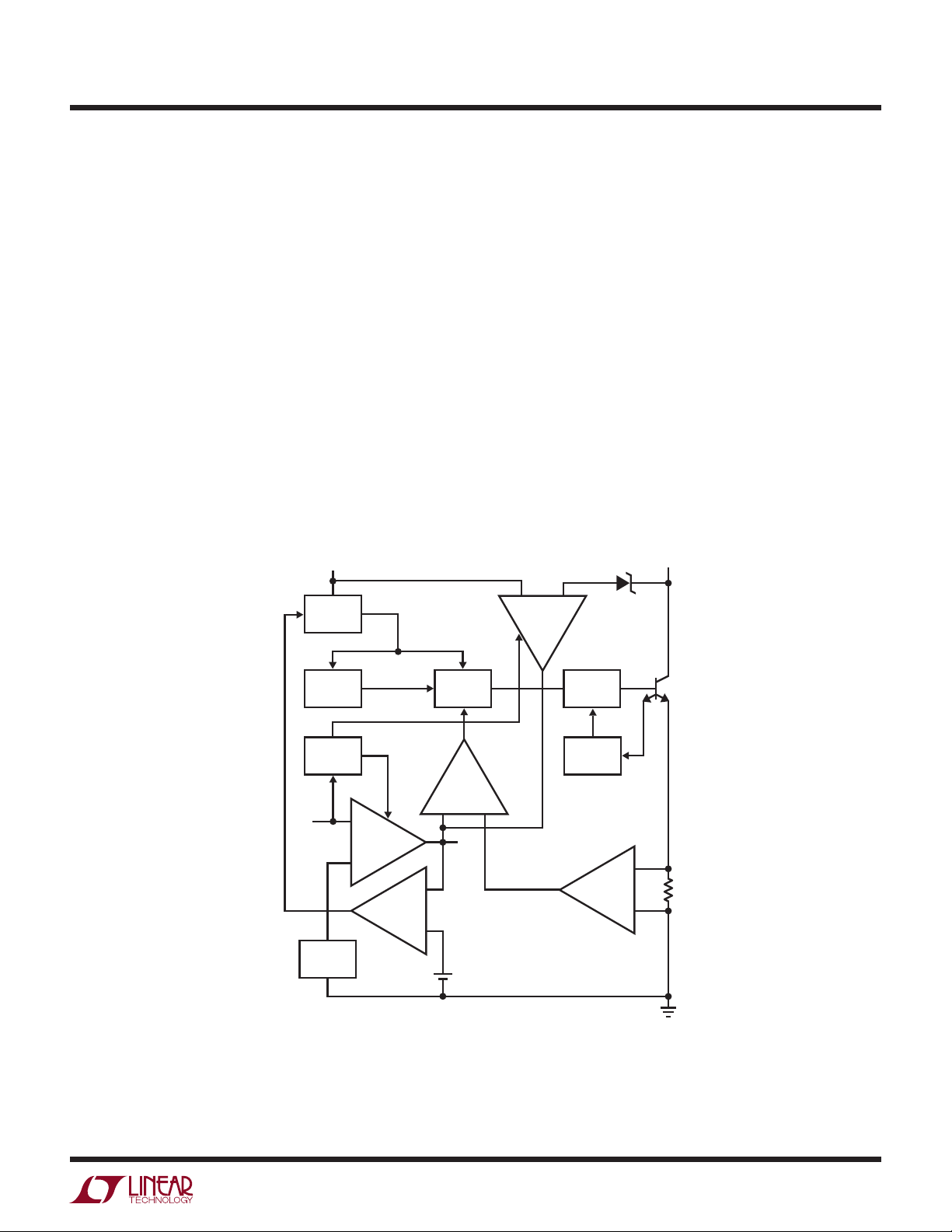
Application Note 29
APPENDIX C
Physiology of the LT1070
The LT1070 is a current mode switcher. This means that
switch duty cycle is directly controlled by switch current
rather than by output voltage. Referring to Figure C1, the
switch is turned on at the start of each oscillator cycle. It
is turned off when switch current reaches a predetermined
level. Control of output voltage is obtained by using the
output of a voltage-sensing error amplifi er to set current
trip level. This technique has several advantages. First,
it has immediate response to input voltage variations,
unlike ordinary switchers which have notoriously poor
line transient response. Second, it reduces the 90° phase
shift at mid-frequencies in the energy storage inductor.
This greatly simplifi es closed-loop frequency compensation under widely varying input voltage or output load
V
IN
conditions. Finally, it allows simple pulse-by-pulse current
limiting to provide maximum switch protection under output overload or short conditions. A low dropout internal
regulator provides a 2.3V supply for all internal circuitry on
the LT1070. This low dropout design allows input voltage
to vary from 3V to 60V with virtually no change in device
performance. A 40kHz oscillator is the basic clock for all
internal timing. It turns on the output switch via the logic
and driver circuitry. Special adaptive antisat circuitry detects onset of saturation in the power switch and adjusts
driver current instantaneously to limit switch saturation.
This minimizes driver dissipation and provides very rapid
turn-off of the switch.
A 1.2V bandgap reference biases the positive input of
the error amplifi er. The negative input is brought out for
output voltage sensing. This feedback pin has a second
function; when pulled low with an external resistor,
SWITCH
OUT
16V
2.3V
REG
40kHz
OSC
MODE
SELECT
FB
1.24V REF
FLYBACK
ERROR
AMP
LOGIC DRIVER
COMP
–
ERROR
+
AMP
V
C
SHUTDOWN
CIRCUIT
+
0.15V
Figure C1. LT1070 Internal Details
ANTI-SAT
CURRENT
GAIN ≈ 6
AMP
5A
75V
SWITCH
+
0.02Ω
–
AN29 FC1
an32f
AN29-37
Page 38

Application Note 29
it programs the LT1070 to disconnect the main error
amplifi er output and connects the output of the fl yback
amplifi er to the comparator input. The LT1070 will then
regulate the value of the fl yback pulse with respect to the
supply voltage. This fl yback pulse is directly proportional
to output voltage in the traditional transformer-coupled
fl yback topology regulator. By regulating the amplitude
of the fl yback pulse the output voltage can be regulated
with no direct connection between input and output. The
output is fully fl oating up to the breakdown voltage of
the transformer windings. Multiple fl oating outputs are
easily obtained with additional windings. A special delay
network inside the LT1070 ignores the leakage inductance
spike at the leading edge of the fl yback pulse to improve
output regulation.
APPENDIX D
The error signal developed at the comparator input is
brought out externally. This pin (V
) has four different
C
functions. It is used for frequency compensation, current
limit adjustment, soft-starting, and total regulator shutdown. During normal regulator operation this pin sits at a
voltage between 0.9V (low output current) and 2.0V (high
output current). The error amplifi ers are current output
) types, so this voltage can be externally clamped
(g
m
for adjusting current limit. Likewise, a capacitor-coupled
external clamp will provide soft-start. Switch duty cycle
goes to zero if the V
diode, placing the LT1070 in an idle mode. Pulling the V
pin is pulled to ground through a
C
C
pin below 0.15V causes total regulator shutdown with only
50μA supply current for shutdown circuitry biasing. For
more details, see Linear Technology Application Note 19,
Pages 4-8.
Inductor Selection for Flyback Converters
A common problem area in DC/DC converter design is the
inductor, and the most common diffi culty is saturation. An
inductor is saturated when it cannot hold any more magnetic
fl ux. As an inductor arrives at saturation it begins to look
more resistive and less inductive. Under these conditions
current fl ow is limited only by the inductor’s DC copper
resistance and the source capacity. This is why saturation
often results in destructive failures.
While saturation is a prime concern, cost, heating, size,
availability and desired performance are also signifi cant.
Electromagnetic theory, although applicable to these issues,
can be confusing, particularly to the non-specialist.
Practically speaking, an empirical approach is often a
good way to address inductor selection. It permits real
time analysis under actual circuit operating conditions
using the ultimate simulator—a breadboard. If desired,
inductor design theory can be used to augment or confi rm
experimental results.
Figure D1 shows a typical fl yback based converter utilizing
the LT1070 switching regulator. A simple approach may
be employed to determine the appropriate inductor. A very
6
useful tool is the #845 inductor kit
shown in Figure D2.
This kit provides a broad range of inductors for evaluation
in test circuits such as Figure D1.
6
Available from Pulse Engineering, Inc., P.O. Box 12235, San Diego, CA
92112, 619-268-2400
1μF
TEST
INDUCTOR
V
SW
FB
10.7k
1.24k
MBR735 (MOTOROLA)
12V OUTPUT
+
470μF
AN29 FD1
5V
22μF
GND
Figure D1. Basic LT1070 Flyback Converter Test Circuit
+
IN
V
IN
LT1070
V
C
+
1k
AN29-38
an32f
Page 39
Application Note 29
Figure D3 was taken with a 450μH value, high core capacity inductor installed. Circuit operating conditions such as
input voltage and loading are set at levels appropriate to
the intended application. Trace A is the LT1070’s V
voltage while Trace B shows its current. When V
SW
SW
pin
pin
voltage is low, inductor current fl ows. The high inductance means current rises relatively slowly, resulting in
the shallow slope observed. Behavior is linear, indicating
no saturation problems. In Figure D4, a lower value unit
with equivalent core characteristics is tried. Current rise
is steeper, but saturation is not encountered. Figure D5’s
selected inductance is still lower, although core characteristics are similar. Here, the current ramp is quite
pronounced, but well controlled. Figure D6 brings some
informative surprises. This high value unit, wound on a
low capacity core, starts out well but heads rapidly into
saturation, and is clearly unsuitable.
The described procedure narrows the inductor choice
within a range of devices. Several were seen to produce
acceptable electrical results, and the “best” unit can be
further selected on the basis of cost, size, heating and other
parameters. A standard device in the kit may suffi ce, or a
derived version can be supplied by the manufacturer.
Using the standard products in the kit minimizes specifi cation uncertainties, accelerating the dialogue between user
and inductor vendor.
A = 20V/DIV
B = 1A/DIV
HORIZ = 5μs/DIV
Figure D4. Waveforms for 170μH, High Capacity Core Unit
AN29 FD4
Figure D2. Model 845 Inductor Selection Kit from Pulse
Engineering, Inc. (Includes 18 Fully Specifi ed Devices)
A = 20V/DIV
B = 1A/DIV
HORIZ = 5μs/DIV
Figure D3. Waveforms for 450μH, High Capacity Core Unit
AN29 FD3
A = 20V/DIV
B = 1A/DIV
HORIZ = 5μs/DIV
Figure D5. Waveforms for 55μH, High Capacity Core Unit
A = 20V/DIV
B = 1A/DIV
HORIZ = 5μs/DIV
Figure D6. Waveforms for 500μH, Low Capacity Core Inductor
(Note Saturation Effects)
AN29 FD5
AN29 FD6
an32f
AN29-39
Page 40

Application Note 29
APPENDIX E
Optimizing Converters for Effi ciency
Squeezing the utmost effi ciency out of a converter is a
complex, demanding design task. Effi ciency exceeding 80%
to 85% requires some combination of fi nesse, witchcraft
and just plain luck. Interaction of electrical and magnetic
terms produces subtle effects which infl uence effi ciency.
A detailed, generalized method for obtaining maximum
converter effi ciency is not readily described but some
guidelines are possible.
Losses fall into several loose categories including junction,
ohmic, drive, switching and magnetic losses.
Semiconductor junctions produce losses. Diode drops
increase with operating current and can be quite costly
in low voltage output converters. A 700mV drop in a
5V output converter introduces more than 10% loss.
Schottky devices will cut this nearly in half, but loss is still
appreciable. Germanium (rarely used) is lower still, but
switching losses negate the low DC drop at high speeds.
In very low power converters Germanium’s reverse leakage may be equally oppressive. Synchronously-switched
rectifi cation is more complex, but can sometimes simulate
a more effi cient diode (see text Figure 32). When evaluating such a scheme remember to include both AC and DC
drive losses in effi ciency estimates. DC losses include
base or gate current in addition to DC consumption in
any driver stage. AC losses might include the effects of
gate (or base) capacitance, transition region dissipation
(the switch spends some time in its linear region) and
power lost due to timing skew between drive and actual
switch action.
device temperature rise. Appropriate tools here include
thermal probes and (at low voltages) the perhaps more
readily available human fi nger. At lower power (e.g., less
dissipation, even though loss percentage may be as great)
this technique is less effective. Sometimes deliberately
adding a known loss to the component in question and
noting effi ciency change allows loss determination.
Ohmic losses in conductors are usually only signifi cant
at higher currents. “Hidden” ohmic losses include socket
and connector contact resistance and equivalent series
resistance (ESR) in capacitors. ESR generally drops with
capacitor value and rises with operating frequency, and
should be specifi ed on the capacitor data sheet. Consider
the copper resistance of inductive components. It is often
necessary to evaluate trade-offs of an inductors copper
resistance versus magnetic characteristics.
Drive losses were mentioned, and are important in obtaining
effi ciency. MOSFET gate capacitance draws substantial AC
drive current per cycle, implying higher average currents as
frequency goes up. Bipolar devices have lower capacitance,
but DC base current eats power. Large area devices may
appear attractive for low saturation, but evaluate drive
losses carefully. Usually, large area devices only make
sense when operating at a signifi cant percentage of rated
current. Drive stages should be thought out with respect
to effi ciency. Class A type drives (e.g., resistive pull-up
or pull-down) are simple and fast, but wasteful. Effi cient
operation usually requires active source-sink combinations
with minimal cross conduction and biasing losses.
Transistor saturation losses are also a signifi cant term.
Channel and collector-emitter saturation losses become
increasingly signifi cant as operating voltages decrease. The
most obvious way to minimize these losses is to select low
saturation components. In some cases this will work, but
remember to include the drive losses (usually higher) for
lower saturation devices in overall loss estimates. Actual
losses caused by saturation effects and diode drops is
sometimes diffi cult to ascertain. Changing duty cycles
and time variant currents make determination tricky. One
simple way to make relative loss judgements is to measure
AN29-40
Switching losses occur when devices spend signifi cant
amounts of time in their linear region relative to operating
frequency. At higher repetition rates transition times can
become a substantial loss source. Device selection and
drive techniques can minimize these losses.
Magnetics design also infl uences effi ciency. Design of
inductive components is well beyond the scope of this appended section, but issues include core material selection,
wire type, winding techniques, size, operating frequency,
current levels, temperature and other issues.
an32f
Page 41

Application Note 29
Some of these topics are discussed in Linear Technology
Application Note 19, but there is no substitute for access
to a skilled magnetics specialist. Fortunately, the other
categories mentioned usually dominate losses, allowing
APPENDIX F
Instrumentation for Converter Design
Instrumentation for DC/DC converter design should be
selected on the basis of fl exibility. Wide bandwidths, high
resolution and computational sophistication are valuable
features, but are usually not required for converter work.
Typically, converter design requires simultaneous observation of many circuit events at relatively slow speeds.
Single ended and differential voltage and current signals
are of interest, with some measurements requiring fully
fl oating inputs. Most low level measurement involves
AC signals and is accommodated with a high sensitivity
plug-in. Other situations call for observation of small,
slowly changing (e.g., 0.1Hz to 10Hz) events on top of DC
levels. This range falls outside the AC-coupled cut-off of
most oscilloscopes, mandating differential DC nulling or
“slide-back” plug-in capability. Other requirements include
high impedance probes, fi lters and oscilloscopes with
very versatile triggering and multi-trace capability. In our
converter work we have found a number of particularly
noteworthy instruments in several categories.
Probes
For many measurements standard 1× and 10× scope
probes are fi ne. In most cases the ground strap may be
used, but low level measurements, particularly in the presence of wideband converter switching noise, should be
taken with the shortest possible ground return. A variety
of probe tip grounding accessories are available, and are
usually supplied with good quality probes (see Figure F1).
In some cases, directly connecting the breadboard to the
‘scope may be necessary (Figure F2).
Wideband FET probes are not normally needed, but a
moderate speed, high input impedance buffer probe is quite
useful. Many converter circuits, especially micropower
designs, require monitoring of high impedance nodes. The
10MΩ loading of standard 10× probes usually suffi ces,
but sensitivity is traded away. 1× probes retain sensitivity,
good effi ciencies to be obtained with standard magnetics.
Custom magnetics are usually only employed after circuit
losses have been reduced to lowest practical levels.
but introduce heavier loading. Figure F3 shows an almost
absurdly simple, but useful, circuit which greatly aids
probe loading problems. The LT1022 high speed FET op
amp drives an LT1010 buffer. The LT1010’s output allows
cable and probe driving and also biases the circuit’s input
shield. This bootstraps the input capacitance, reducing its
effect. DC and AC errors of this circuit are low enough for
almost all converter work, with enough bandwidth for most
circuits. Built into a small enclosure with its own power
supply, it can be used ahead of a ‘scope or DVM with good
results. Pertinent specifi cations appear in the diagram.
Figure F4 shows a simple probe fi lter which sets high and
low bandwidth restrictions. This circuit, placed in series
with the ‘scope input, is useful for eliminating switching
artifacts when observing circuit nodes.
An isolated probe allows fully fl oating measurements,
even in the presence of high common mode voltages. It
is often desirable to look across fl oating points in a circuit.
The ability to directly observe an ungrounded transistor’s
saturation characteristics or monitor waveforms across a
fl oating shunt makes this probe valuable. One probe, the
Signal Acquisition Technologies, Inc. Model SL-10, has
10MHz bandwidth and 600V common mode capability.
Current probes are an indispensable tool in converter
design. In many cases current waveforms contain more
valuable information than voltage measurements. The
clip-on types are quite convenient. Hall effect based versions respond down to DC, with bandwidths of 50MHz.
Transformer types are faster, but roll off below several
hundred cycles (Figure F5). Both types have saturation
limitations which, when exceeded, cause odd results
on the CRT, confusing the unwary. The Tektronix P6042
(and the more recent AM503) Hall type and P6022/134
transformer based type give excellent results. The HewlettPackard 428B clip-on current probe responds from DC
an32f
AN29-41
Page 42

Application Note 29
Figure F1. Proper Probing Technique for Low Level Measurements in the Presence of High Frequency Noise
AN29-42
Figure F2. Direct Connections to the Oscilloscope Give Best Low Level Measurements.
Note Ground Reference Connection to the Differential Plug-In’s Negative Input
an32f
Page 43

Application Note 29
to only 400Hz, but features 3% accuracy over a 100μA
to 10A range. This instrument, useful for determining effi ciency and quiescent current, eliminates shunt caused
measurement errors.
Oscilloscopes and Plug-Ins
The oscilloscope plug-in combination is an important
choice. Converter work almost demands multi-trace capability. Two channels are barely adequate, with four far
preferable. The Tektronix 2445/6 offers four channels, but
two have limited vertical capability. The Tektronix 547 (and
18V
–
CLIP
INPUTS
LT1022 LT1010
+
–18V
the more modern 7603), equipped with a type 1A4 (2 dual
trace 7A18s required for the 7603) plug-in, has four full
capability input channels with fl exible triggering and superb
CRT trace clarity. This instrument, or its equivalent, will
handle a wide variety of converter circuits with minimal
restrictions. The Tektronix 556 offers an extraordinary
array of features valuable in converter work. This dual
beam instrument is essentially two fully independent
oscilloscopes sharing a single CRT. Independent vertical,
horizontal and triggering permit detailed display of almost
any converters operation. Equipped with two type 1A4
10k
1000pF
OUTPUT
AN29 FF3
INPUT CAPACITANCE ≈ 8pF
= 50pA
I
B
GBW = 8.5MHz
SLEW = 23V/μs
OFFSET VOLTAGE = 250μV
OFFSET TEMPERATURE DRIFT = 5μV/°C
Figure F3. A Simple High Impedance Probe
OUT
160pF
100kHz
0.0016
10kHz
HIGH PASS
LOW PASS
1kHz100Hz10Hz
BNC INPUT
(TO PROBE)
0.016
1kHz
0.16μF
16k
0.0010.010.11μF
100kHz10kHz
100Hz
1.6μF
10Hz
100pF
OUT
Figure F4. Oscilloscope Filter
BNC OUTPUT
(TO SCOPE)
1MSCOPE
AN29 FF4
C
SMALL
TYPICALLY
9pF TO 22pF
an32f
AN29-43
Page 44
Application Note 29
plug-ins, the 556 will display eight real time inputs. The
independent triggering and time bases allow stable display
of asynchronous events. Cross beam triggering is also
available, and the CRT has exceptional trace clarity.
Two oscilloscope plug-in types merit special mention.
At low level, a high sensitivity differential plug-in is indispensable. The Tektronix 1A7 and 7A22 feature 10μV
sensitivity, although bandwidth is limited to 1MHz. The
A = 100mA/DIV
B = 100mA/DIV
HORIZ = 2ms/DIV
Figure F5. Hall (Trace A) and Transformer (Trace B) Based
Current Probes Responding to Low Frequency
AN29 FF5
units also have selectable high and low pass fi lters and
good high frequency common mode rejection. Tektronix
types W, 1A5 and 7A13 are differential comparators. They
have calibrated DC nulling (“slideback”) sources, allowing observation of small, slowly moving events on top of
common mode DC.
Voltmeters
Almost any DVM will suffi ce for converter work. It should
have current measurement ranges and provision for
battery operation. The battery operation allows fl oating
measurements and eliminates possible ground loop errors. Additionally, a non-electronic (VOM) voltmeter (e.g.,
Simpson 260, Triplett 630) is a worthwhile addition to the
converter design bench. Electronic voltmeters are occasionally disturbed by converter noise, producing erratic
readings. A VOM contains no active circuitry, making it
less susceptible to such effects.
APPENDIX G
The Magnetics Issue
Magnetics is probably the most formidable issue in
converter design. Design and construction of suitable
magnetics is a diffi cult task, particularly for the non-specialist. It is our experience that the majority of converter
design problems are associated with magnetics requirements. This consideration is accented by the fact that
most converters are employed by non-specialists. As a
Figure G1. Magnetics for LTC Applications Circuits are Designed
and Supplied as Standard Product by Pulse Engineering, Inc.
purveyor of switching power ICs we incur responsibility
towards addressing the magnetics issue (our publicly
spirited attitude is, admittedly, capitalistically infl uenced).
As such, it is LTC’s policy to use off-the-shelf magnetics
in our circuits. In some cases, available magnetics serve
a particular design. In other situations the magnetics have
been specially designed, assigned a part number and
made available as standard product. In these endeavors
our magnetics supplier and partner is;
Pulse Engineering, Inc.
P.O. Box 12235
7250 Convoy Court
San Diego, California 92112
619-268-2400
In many circumstances a standard product is suitable
for production. Other cases may require modifi cations or
changes which Pulse Engineering can provide. Hopefully,
this approach serves the needs of all concerned.
AN29-44
an32f
Page 45

APPENDIX H
Application Note 29
LT1533 Ultralow Noise Switching Regulator for High
Voltage or High Current Applications
1, 2
The LT1533 switching regulator
achieves 100μV output noise by using closed-loop control around its output
switches to tightly control switching transition time. Slowing down switch transitions eliminates high frequency
harmonics, greatly reducing conducted and radiated noise.
The part’s 30V, 1A output transistors limit available power.
It is possible to exceed these limits while maintaining low
noise performance by using suitably designed output
stages.
High Voltage Input Regulator
The LT1533’s IC process limits collector breakdown to
30V. A complicating factor is that the transformer causes
the collectors to swing to twice the supply voltage. Thus,
15V represents the maximum allowable input supply. Many
applications require higher voltage inputs; the circuit in
3
Figure H1 uses a cascoded
high voltage capability. This 24V to 5V (V
output stage to achieve such
= 20V–50V)
IN
converter is reminiscent of previous LT1533 circuits,
4
except for the presence of Q1 and Q2.
These devices,
interposed between the IC and the transformer, constitute
a cascoded high voltage stage. They provide voltage gain
while isolating the IC from their large drain voltage swings.
Normally, high voltage cascodes are designed to simply
supply voltage isolation. Cascoding the LT1533 presents
special considerations because the transformer’s instantaneous voltage and current information must be accurately
transmitted, albeit at lower amplitude, to the LT1533. If
this is not done, the regulator’s slew-control loops will
not function, causing a dramatic output noise increase.
The AC-compensated resistor dividers associated with the
T1
6
7
5
24V
IN
(20V TO 50V)
Q3
MPSA42
+
4.7μF
0.002μF
1500pF
18k
0.01μF
220Ω
10k
Q4
2N2222
L1, L3: COILTRONICS CTX100-3
L2: 22nH TRACE INDUCTANCE, FERRITE BEAD OR
INDUCTOR COILCRAFT B-07T TYPICAL
Q1, Q2: MTD6N15
T1: COILTRONICS VP4-0860
8
+
10μF
10k
1k
14
V
IN
4
SYNC
3
DUTY
11
SHDN
5
C
T
6
R
T
10
V
C
GND
220Ω
0.002μF
Q1
215
COL A
9
LT1533
R
CSL
Q2
COL B
PGND
NFB
FB
R
VSL
13
12
12k
10k
4
9
3
MBRS140
10
10k
16
8
7
1
12
1k
2
MBRS140
11
L2
L1
100μH
7.5k
1%
2.49k
1%
AN29 FH1
L3
5V
OUT
+
OPTIONAL
100μH
SEE TEXT
+
220μF
AN70 F40
100μF
Figure 1H. A Low Noise 24V to 5V Converter (VIN = 20V–50V): Cascoded MOSFETs
Withstand 100V Transformer Swings, Permitting the LT1533 to Control 5V/2A Output
Information furnished by Linear Technology Corporation is believed to be accurate and reliable.
However, no responsibility is assumed for its use. Linear Technology Corporation makes no representation that the interconnection of its circuits as described herein will not infringe on existing patent rights.
an32f
AN29-45
Page 46

Application Note 29
Q1–Q2 gate-drain biasing serve this purpose, preventing
transformer swings coupled via gate-channel capacitance
from corrupting the cascode’s waveform-transfer fidelity.
Q3 and associated components provide a stable DC termination for the dividers while protecting the LT1533 from
the high voltage input.
Figure H2 shows that the resultant cascode response is
faithful, even with 100V swings. Trace A is Q1’s source;
traces B and C are its gate and drain, respectively. Under
these conditions, at 2A output, noise is inside 400μV peak.
Current Boosting
Figure H3 boosts the regulator’s 1A output capability
to over 5A. It does this with simple emitter followers
(Q1–Q2). Theoretically, the followers preserve T1’s voltage
and current waveform information, permitting the LT1533’s
slew-control circuitry to function. In practice, the transistors must be relatively low beta types. At 3A collector
current, their beta of 20 sources ≈150mA via the Q1–Q2
5
base paths, adequate for proper slew-loop operation.
The follower loss limits effi ciency to about 68%. Higher
input voltages minimize follower-induced loss, permitting
efficiencies in the low 70% range.
Figure H4 shows noise performance. Ripple measures 4mV
(Trace A) using a single LC section, with high frequency
content just discernible. Adding the optional second LC
section reduces ripple to below 100μV (trace B), and high
frequency content is seen to be inside 180μV (note ×50
vertical scale-factor change).
1
Witt, Jeff. The LT1533 Heralds a New Class of Low Noise Switching
Regulators. Linear Technology VII:3 (August 1997).
2
Williams, Jim. LTC Application Note 70: A Monolithic Switching Regulator
with 100μV Output Noise. October 1997.
3
The term “cascode,” derived from “cascade to cathode,” is applied
to a configuration that places active devices in series. The benefit may
be higher breakdown voltage, decreased input capacitance, bandwidth
improvement or the like. Cascoding has been employed in op amps,
power supplies, oscilloscopes and other areas to obtain performance
enhancement.
4
This circuit derives from a design by Jeff Witt of Linear Technology Corp.
5
Operating the slew loops from follower base current was suggested by
Bob Dobkin of Linear Technology Corp.
A = 20V/DIV
B = 5V/DIV
AC-COUPLED
C = 100V/DIV
10μs/DIV
AN29 FH2
Figure H2. MOSFET-Based Cascode Permits the Regulator to
Control 100V Transformer Swings While Maintaining a Low
Noise 5V Output. Trace A Is Q1’s Source, Trace B Is Q1’s Gate
and Trace C Is the Drain. Waveform Fidelity Through Cascode
Figure H4. Waveforms for Figure H3 at 10W Output: Trace A
Shows Fundamental Ripple with Higher Frequency Residue
Just Discernible. The Optional LC Section Results in Trace B’s
180μV
A = 5mV/DIV
B = 100μV/DIV
2μs/DIV
Wideband Noise Performance
P-P
AN29 FH4
Permits Proper Slew-Control Operation
1N4148
Q1
Q2
1N4148
330Ω
0.05Ω
0.05Ω
330Ω
1N5817
T1
0.003μF
680Ω
1N5817
L1
300μH
AN29 FH3
L3
12V
+ +
()
33μH
100μF
OPTIONAL FOR
LOWEST RIPPLE
100μF
5V
+
4.7μF
11
3
4
1500pF
5
18k
6
10
0.01μF
SHDN
DUTY
SYNC
C
T
R
V
14
V
IN
2
COL A
15
COL B
16
PGND
LT1533
T
C
GND
NFB
13
R
VSL
12
R
CSL
7
FB
89
10k
10k
L2
R2
2.49k
1%
+
4.7μF
R1
21.5k
1%
L1: COILTRONICS CTX300-4
L2: 22nH TRACE INDUCTANCE, FERRITE BEAD OR
INDUCTOR. COILCRAFT B-07T TYPICAL
L3: COILTRONICS CTX33-4
Q1, Q2: MOTOROLA D45C1
T1: COILTRONICS CTX-02-13949-X1
: FERRONICS FERRITE BEAD 21-110J
Figure H3. A 10W Low Noise 5V to 12V Converter: Q1–Q2 Provide 5A Output Capacity While Preserving the LT1533’s Voltage/Current
Slew Control. Efficiency Is 68%. Higher Input Voltages Minimize Follower Loss, Boosting Efficiency Above 71%
IM/GP 689 5K • PRINTED IN USA
AN29-46
Linear Technology Corporation
1630 McCarthy Blvd., Milpitas, CA 95035-7417
(408) 432-1900 ● FAX: (408) 434-0507
●
www.linear.com
© LINEAR TECHNOLOGY CORPORATION 1989
an32f
 Loading...