

Page 1
Application Note 27A
June 1988
A Simple Method of Designing Multiple Order All Pole
Bandpass Filters by Cascading 2nd Order Sections
Nello Sevastopoulos
Richard Markell
INTRODUCTION
Filter design, be it active, passive, or switched capacitor,
is traditionally a mathematically intensive pursuit. There
are many architectures and design methods to choose
from. Two methods of high order bandpass filter design
are discussed herein. These methods allow the filter
designer to simplify the mathematical design process
®
and allow LTC’s switched capacitor filters (LTC
1059,
LTC1060, LTC1061,LTC1064) to be utilized as high quality
bandpass filters.
The first method consists of the traditional cascading of
non-identical 2nd order bandpass sections to form the
familiar Butterworth and Chebyshev bandpass filters.
The second method consists of cascading identical 2nd
order bandpass sections. This approach, although “nontextbook,” enables the hardware to be simple and the
mathematics to be straightforward. Both methods will
be described here.
AN27A is the first of a series of application notes from
LTC concerning our universal filter family. Additional notes
in the series will discuss notch, lowpass and highpass
filters implemented with the universal switched capacitor
filter. An addition to this note will extend the treatment of
bandpass filters to the elliptic or Cauer forms.
This note will first present a finished design example and
proceed to present the design methodology, which relies on
tabular simplification of traditional filter design techniques.
DESIGNING BANDPASS FILTERS
Table 1 was developed to enable anyone to design Butterworth bandpass filters. We will discuss the tables in
more detail later in this paper, but let’s first design a filter.
EXAMPLE 1—DESIGN
A 4th order 2kHz Butterworth bandpass filter with a –3dB
bandwidth equal to 200Hz is required as shown in Figure 1.
Noting that (f
/BW) = 10/1 we can go directly to Table1
oBP
for our normalized center frequencies. From Table 1
under 4th order Butterworth bandpass filters, we go to
/BW) = 10.
(f
oBP
L, LT, LTC, LTM, Linear Technology and the Linear logo are registered trademarks of Linear
Technology Corporation. All other trademarks are the property of their respective owners.
0
–3
–10
–20
–30
GAIN (dB)
–40
–50
–60
0.5k 0.7k 1k 2k 3k 4k 5k
Figure 1. 4th Order Butterworth BP Filter, f
FREQUENCY (Hz)
200Hz
AN27A F01
oPB
10k
= 2kHz
an28f
AN27A-1
Page 2
Application Note 27A
We find fo1 = 0.965 and fo2 = 1.036 (both normalized to
= 1). To find our desired actual center frequencies,
f
oBP
we must multiply by f
and f
The Qs are Q
= 2.072kHz.
o2
1
= Q2 = 14.2 which is read directly from
= 2kHz to obtain fo1 = 1.930kHz
oBP
Table 1. Also available from the table is K, which is the
product of each individual bandpass gain H
. To put it
oBP
another way, the value of K is the gain required to make
the gain, H, of the overall filter equal to 1 at f
. Our filter
oBP
parameters are highlighted in the following table:
f
oBP
2kHz 1.93kHz 2.072kHz Q1 = Q2 = 14.2 2.03
f
o1
f
o2
Qs K
HARDWARE IMPLEMENTATION
Universal switched capacitor filters are simple to implement. A bandpass filter can be built from the traditional
state-variable filter topology. Figure 2 shows this topology
for both switched capacitor and active operational amplifier
implementations. Our example requires four resistors for
each 2nd order section. So eight resistors are required
to build our filter.
We start with two 2nd order sections (1 LTC1060,
2/3 LTC1061 or 1/2 LTC1064), Figure 3.
We associate resistors as belonging to 2nd order sections,
so R1x belongs to the x section. Thus R12, R22, R33 and
R42 all belong to the second of two 2nd order sections
in our example.
Our requirements are shown in the following table:
SECTION 1 SECTION 2
= 1.93kHz
f
o1
Q1 = 14.2
H
= 1
oBP1
Note that H
choosing H
oBP1
oBP2
× H
oBP2
= 2.03.
= K and this is the reason for
For this example we choose the fo=
= 2.072kHz
f
o2
Q2 = 14.2
H
= 2.03
oBP2
f
CLK
50
R2
R4
mode,
so we will tie the 50/100/Hold pin on the SCF chip to V+,
generally (5V to 7V). We choose 100kHz as our clock and
calculate resistor values. Choosing the nearest 1% resistor
values we can implement the filter using Figure3’s topology and the resistor values listed below.
R11 = 147k R12 = 71.5k
R21 = 10k R22 = 10.7k
R31 = 147k R32 = 147k
R41 = 10.7k R42 = 10k
Our design is now complete. We have only to generate a
TTL or CMOS compatible clock at 100kHz, which we feed
to the clock pin of the switched capacitor filter, and we
should be “on the air.”
STATE VARIABLE SCF ACTIVE (OP-AMP) STATE VARIABLE
R4
R3
R2 R2
HP
R1
V
IN
–
+
AGND
f
R2
R3
fo=
CLK
100(50)
|
R4
Q =
R2
|
H
oHP
R2
R4
S BP LP
–
+
1/2 LTC1060
1/3 LTC1061
1/4 LTC1064
= –R2 /R1 H
MODE 3
∫ ∫
= –R3 /R1 H
oBP
oLP
= –R4 /R1
R1
V
IN
–
R5
+
1
fO=
2πRC
Figure 2. Switched Capacitor vs Active RC State Variable Topology
AN27A-2
R4
C
C
R
–
R
–
+
R6
3/4 LTC1014
R2
R4
+
AN27A F02
an28f
Page 3
Application Note 27A
R41
R31
R21
R11
V
IN
–
+
fo=
f
CLK
50
R3
R2
; Q=
R2
R4
Figure 3. Two 2nd Order Sections Cascaded to Form 4th Order BP Filiter
HP
–
+
–
1/2 LTC1060
R2
H
oBP
R4
S1
A
∫ ∫
= –R3 /R1
BP
LP
DESIGNING BANDPASS FILTERS—THEORY BEHIND
THE DESIGN
Traditionally, bandpass filters have been designed by laborious calculations requiring some time to complete. At the
present time programs for various personal or laboratory
computers are often used. In either case, no small amount
of time and/or money is involved to evaluate, and later
test, a filter design.
R42
R32
R12
R22
–
+
HP
–
+
–
1/2 LTC1060
S1
A
∫ ∫
BP
LP
BP
OUTPUT
AN27A F03
with the required characteristics (generally the Qs are too
high). We wish to explore here the use of cascaded identical
2nd order sections for building high Q bandpass filters.
For a 2nd order bandpass filter
2
1–G
Q =
G
×
1– f /f
f/f
o
( )
o
2
(1)
Many designers have inquired as to the feasibility of cascading 2nd order bandpass sections of relatively low Q to
obtain more selective, higher Q, filters. This approach is
ideally suited to the LTC family of switched capacitor filters
(LTC1059, LTC1060, LTC1061 and LTC1064). The clock
to center frequency ratio accuracy of a typical “Mode1”
design with non “A” parts is better than 1% in a design
that simply requires three resistors of 1% tolerance or
better. Also, no expensive high precision film capacitors
are required as in the active op amp state variable design.
We present here an approach for designing bandpass filters
using the LTC1059, LTC1060, LTC1061 or the LTC1064
which many designers have “on the air” in days instead
of weeks.
CASCADING IDENTICAL 2ND ORDER BANDPASS SECTIONS
When we want to detect single frequency tones and simultaneously reject signals in close proximity, simple 2nd
order bandpass filters often do the job. However, there are
cases where a 2nd order section cannot be implemented
Where Q is the required filter quality factor
f is the frequency where the filter should have gain, G,
expressed in Volts/V.
is at the filter center frequency. Unity gain is assumed
f
o
.
at f
o
EXAMPLE 2—DESIGN
We wish to design a 2nd order BP filter to pass 150Hz
and to attenuate 60Hz by 50dB. The required Q may be
calculated from Equation (1):
2
So,Q =
1– 3.162× 10
( )
3.162× 10
–3
–3
60 /150
×
1– 60/ 150
( )
= 150.7
2
This very high Q dictates a –3dB bandwidth of 1Hz.
Although the universal switched capacitor filters can
realize such high Qs, their guaranteed center frequency
accuracy of ±0.3%, although impressive, is not enough to
pass the 150Hz signal without gain error. According to the
an28f
AN27A-3
Page 4
Application Note 27A
f
–R3
R3
previous equation, the gain at 150Hz will be 1 ±26%; the
rejection, however, at 60Hz will remain at –50dB. The gain
inaccuracy can be corrected by tuning resistor R4 when
mode 3, Figure 2, is used. Also, if only detection of the
signal is sought, the gain inaccuracy could be acceptable.
This high Q problem can be solved by cascading two identical 2nd order bandpass sections. To achieve a gain, G, at
frequency f the required Q of each 2nd order section is:
1–G
Q =
G
×
1– f / f
f / f
o
( )
o
2
(2)
The gain at each bandpass section is assumed unity.
In order to obtain 50dB attenuation at 60Hz, and still pass
150Hz, we will use two identical 2nd order sections.
We can calculate the required Q for each of two 2nd order
sections from Equation (2):
So,Q =
1–3.162× 10
3.162× 10
–3
–3
×
60 /150
1– 60/ 150
( )
= 8.5!!
2
With two identical 2nd order sections each with a potential error in center frequency, f
, of ±0.3% the gain error
o
at 150Hz is 1 ±0.26%. If lower cost (non “A” versions
of LTC1060 and LTC1064) 2nd order bandpass sections
are used with an fo tolerance of ±0.8%, the gain error at
150Hz is 1 ±1.8%! The benefits of lower Q sections are
therefore obvious.
HARDWARE IMPLEMENTATION
Mode 1 Operation of LTC1060, LTC1061, LTC1064
As previously discussed, we associate resistors with each
2nd order section, so R1x belongs to x section. Thus R12,
R22 and R23 belong to the second of the two 2nd order
sections, Figure 4.
Each section has the same requirements as shown:
= fo2 = 150Hz
f
o1
Q1 = Q = 8.5
H
oBP1
= H
oBP2
= 1
Note that we could get gain out of our BP filter structure
by letting the product of the H
terms be >1 (within the
oBP
performance limits of the filter itself).
For our example using the LTC1060 we will use f
/100. So we input a 15kHz clock and tie the 50/100/
= f
CLK
= fo2
o1
Hold pin to mid-supplies (ground for ±5V supplies).
We can implement this filter using the two sections of an
LTC1060 filter operated in mode 1. Mode 1 is the fastest
operating mode of the switched capacitor filters. It provides
Lowpass, Bandpass and Notch outputs.
Each 2nd order section will perform approximately as
shown in Figure 5, curve (a).
Implementation in mode 1 is simple as only three resistors
are required per section. Since we are cascading identical
sections, the calculations are also simple.
R31
R21
R11
V
IN
AN27A-4
–
+
AGND AGND
CLK
fo=
H
=
oBP
100
R1
S
N
–
+
1/2 LTC1060 1/2 LTC1060
Q =
∫ ∫
–
R2
Figure 4. LTC1060 as BP Filter Operating in Mode 1
BP
LP
R12
R32
R22
–
+
S
N
–
+
∫ ∫
–
BP
AN27A F04
LP
BP
OUTPUT
an28f
Page 5
Application Note 27A
( )
We can calculate the resistor values from the indicated
formulas and then choose 1% values. (Note that we let
our minimum value be 20k.) The required values are:
R11 = R12 = 169k
R21 = R22 = 20k
R31 = R32 = 169k
Our design is complete. The performance of two 2nd order
sections cascaded versus one 2nd order section is shown
in Figure 5, curve (b). We must, however, generate a TTL
or CMOS clock at 15kHz to operate the filter.
Mode 2 Operation of LTC1060 Family
Suppose that we have no 15kHz clock source readily available. We can use what is referred to as mode 2, which
allows the input clock frequency to be less than 50:1 or
0
–10
–20
–30
–40
BANDPASS GAIN (dB)
–50
–60
30 50 100 150 300 500
FREQUENCY (Hz)
Figure 5. Cascading Two 2nd Order BP Sections for Higher
Q Response
(a): ONE SECTION
(b): TWO SECTIONS
1k
AN27A F05
100:1 [f
= 50 or 100]. This still depends on the con-
CLK/fo
nection of the 50/100/Hold pin.
If we wish to operate our previous filter from a television
crystal at 14.318MHz we could divide this frequency by
1000 to give us a clock of 14.318kHz. We could then set
up our mode 2 filter as shown in Figure 6.
We can calculate the resistor values from the formulas
shown and then choose 1% values. The required values are:
R11, R12 = 162k
R21, R22 = 20k
R31, R32 = 162k
R41, R42 = 205k
CASCADING MORE THAN TWO IDENTICAL 2ND ORDER BP SECTIONS
If more than two identical bandpass sections (2nd order)
are cascaded, the required Q of each section may be
shown to be:
2/n
1–G
Q =
1/n
G
where Q, G, f and f
f / f
1– f / f
( )
o
2
o
×
are as previously defined and n = the
o
(3)
number of cascaded 2nd order sections.
R41
R31
R21
R11
V
IN
–
+
f
R2
CLK
fo=
1+
Q =
R4
100
H
=R3/ R1
oBP
N
–
+
–
1/2 LTC1060
R3
R2
1+
R2
R4
S
∫ ∫
BP
LP
R12
R42
R32
R22
S
N
BP
LP
–
–
+
+
1/2 LTC1060
∫ ∫
–
BP
OUTPUT
AN27A F06
Figure 6. LTC1060 as BP Filter Operating in Mode 2
an28f
AN27A-5
Page 6

Application Note 27A
( )
( )
The equivalent Q of the overall bandpass filter is then:
Q
identical section
Q
equiv
( )
=
1/n
2
( )
(4)
–1
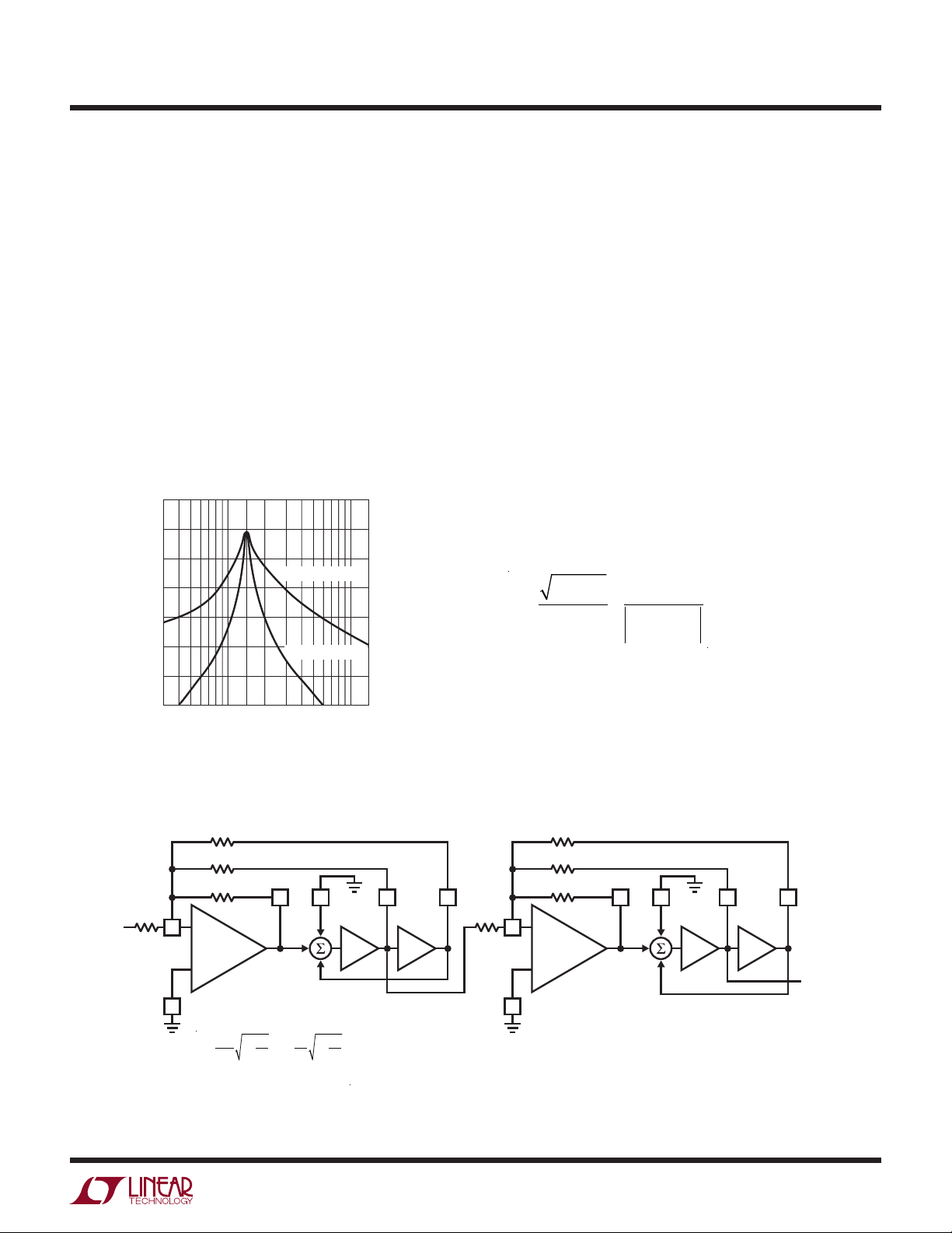
Figure 7 shows the passband curves for Q = 2 cascaded
bandpass sections where n is the number of 2nd order
sections cascaded.
The benefits can be seen for two and three cascaded sections. Cascading four or more sections increases the Q,
but not as rapidly. Nevertheless for designers requiring
high Q bandpass filters cascading identical sections is a
very real option considering the simplicity.
SIMPLE 2ND ORDER BANDPASS FILTERS
Gain and Phase Relations
The bandpass output of each 2nd order filter section of
the LTC1059, LTC1060, LTC1061 and LTC1064, closely
approximates the gain and phase response of an ideal
“textbook” filter.
0
–3
–5
N = 1
–10
N = 2
–15
–20
GAIN (dB)
–25
–30
–35
–40
0.4 0.6 0.8 1 1.2 1.4 1.6
N = 3
N = NUMBER OF SECOND ORDER
N = 4
Q = 2, BANDPASS SECTIONS
NORMALIZED FREQUENCY
AN27A F07
Figure 7. Frequency Response of n Cascaded Identical 2nd Order
Bandpass Sections
frequency and Q drift, but for system considerations,
this may not be practical.
BANDPASS OUTPUT
H
oBP
0.707 H
oBP
GAIN (V/V)
× ff
H
G =
oBP
2
2
– f
f
( )
o
2
+ ffo/ Q
/Q
o
( )
1/2
2
G = filter gain in Volts/V
f0 = the filter’s center frequency
Q = the quality coefficient of the filter
HoBP = the maximum voltage gain of the filter
occurring at f
f
o
= –3dB bandwidth of the filter
O
Q
Figure 8 illustrates the above definitions. Figure 9 illustrates the bandpass gain, G, for various values of Q. This
figure is very useful for estimating the filter attenuation
when several identical 2nd order bandpass filters are
cascaded. High Qs make the filter more selective, and
at the same time, more noisy and more difficult to realize. Qs in excess of 100 can be easily realized with the
universal switched capacitor filters, LTC1059, LTC1060,
LTC1061 and LTC1064, and still maintain low center
f
fHf
L
o
f(LOG SCALE)
f
o
Q =
; fo= fLf
H
L
2
1
+
1
+
+1
2Q
2
1
+1
2Q
fL= f
f
H
fH– f
–1
o
2Q
= f
o
2Q
Figure 8. Bandpass Filter Parameters
0
–10
Q = 1
–20
–30
–40
–50
BANDPASS GAIN (dB)
–60
–70
–80
Q = 10
Q = 20
0.1 0.3 0.50.7
Q = 2
Q = 3
Q = 5
NORMALIZED FREQUENCY
1 3 5 7 10
AN27A F09
Figure 9. Bandpass Gain as a Function of Q
an28f
AN27A-6
Page 7

Application Note 27A
The phase shift, φ, of a 2nd order bandpass filter is:
2
φ = – arctan
2
f
– f
o
ff
o
× Q
The phase shift at fo is 0° or, if the filter is inverting,
it is –180°. All the bandpass outputs of the LTC1059,
LTC1060, LTC1061 and LTC1064 universal filters are
inverting. The phase shift, especially in the vicinity of f
,
o
depends on the value of Q, see Figure 10. By the same
argument, the phase shift at a given frequency varies
from device to device due to the fo tolerance. This is
true especially for high Qs and in the vicinity of f
. For
o
instance, an LTC1059A, 2nd order universal filter, has a
guaranteed initial center frequency tolerance of ±0.3%.
The ideal phase shift at the ideal fo should be –180°. With
a Q of 20, and without trimming, the worst-case phase
shift at the ideal f
will be –180° ±6.8°. With a Q of 5
o
the phase shift tolerance becomes –180° ±1.7°. These
are important considerations when bandpass filters are
used in multichannel systems where phase matching is
required. By way of comparison, a state variable active
bandpass filter built with 1% resistors and 1% capacitors
may have center frequency variation of ±2% resulting in
phase variations of ±2% resulting in phase variations of
±33.8° for Q = 20 and ±11.4° for Q = 5.
Constant Q Versus Constant BW
The bandpass outputs of the universal filters are “constant
Q.” For instance, a 2nd order bandpass filter operating
in mode 1 with a 100kHz clock (see LTC1060 data sheet)
ideally has a 1kHz or 2kHz center frequency, and a –3dB
bandwidth equal to (f
/Q). When the clock frequency
o
varies, the center frequency and bandwidth will vary
at the same rate. In a constant bandwidth filter, when
the center frequency varies, the Q varies accordingly to
maintain a constant (f
/Q) ratio. A constant bandwidth
o
BP filter could be implemented using 2nd order switched
capacitor filters but this is beyond the scope of this paper.
0
±10°
±20°
±30°
±40°
φ
±50°
±60°
±70°
±80°
±90°
0.2 0.4 0.6 0.8 1.0
0
Figure 10. Phase Shift, φ, of a 2nd Order BP Filter Section (LTC1059, 1/2 LTC1060, 1/3 LTC1061)
f/f
o
Q = 1
Q = 10
1.2 1.4 1.6 1.8 2.0
AN27A F10
an28f
AN27A-7
Page 8

Application Note 27A
f
BW
1
2
2
( )
Using The Tables
Tables 1 through 4 were derived from textbook filter theory.
They can be easily applied to the LTC filter family (LTC1059,
LTC1060, LTC1061 and LTC1064) if the Qs are kept relatively
low (<20) and the tuning resistors are at least 1% tolerance. These lower Q designs provide almost textbook BP
filter performance using LTC’s switched capacitor filters.
For higher Q implementations, tuning should be avoided
and the “A” versions of the LTC1059, LTC1060, LTC1061
or LTC1064 should be specified. Also, resistor tolerances
of better than 1% are a necessity.
Table 1 may be used to find pole positions and Qs for
Butterworth bandpass filters. It should be noted that
the bandpass filters in these tables are geometrically
symmetrical about their center frequencies, f
frequency,f
counterpart f
f4=
, as shown in Figure 11 has its geometrical
3
such that:
4
2
f
oBP
f
3
BP. Any
o
Additionally, Table 1 illustrates the attenuation at the
frequencies f
, f5, f7 and f9, which correspond to band-
3
widths 2, 3, 4 and 5 times the passband (see Figure 11).
These values allow the user to get a good estimate of
filter selectivity,
This is true for any bandwidth, BW, and any set of frequencies. The tables can now be arithmetically scaled as
illustrated.
0
–3
A2
A3
GAIN (dB)
A4
A5
f
f
9
7f5f3f1
FREQUENCY (LOG SCALE)
( )
2
( )
x+1
2
+4 f
( )
x+1
PAIR,ANYBW
±BW+ BW
f1,f
=
( )
2
MORE GENERALLY fx,f
VALID FOR ANY fx,f
( )
Figure 11. Generalized Bandpass Butterworth Response
(See Table 1)
0
–2
BW
2BW
3BW
4BW
5BW
f
oBP
2
oBP
±nBW+ nBW
=
BW
f2f4f6f8f
2
+4 f
( )
( )
2
oBP
f2– f
=BW
1
= f
f
1f2
oBP
AN27A F11
10
2
An important approximation can be made for not only the
Butterworth filters in Table 1, but also for the Chebyshev
filter Tables 2, 3 and 4. Treating Figure 11 (or Figure 12) as
a generalized bandpass filter, the two corner frequencies f
can be seen to be nearly arithmetically symmetrical
and f
1
with respect to f
oPB
>>
provided that:
oBP
, BW = f2– f
1
2
Under this condition, for either Butterworth or Chebyshev
bandpass filters:
f
– f
3
f
oBP
f
oPB
4
≅
≅
+ f
2
f
– f
5
3
6
+ f
5
•
•
•
A2
GAIN (dB)
A3
A4
A5
f
9
f4f3= f
oPB
±2BW+ 2BW
f4,f
=
( )
3
FOR ANY fx,f
ANY CORRESPONDING BANDWIDTH
2BW, 3BW, ETC.
( )
FOR EXAMPLE:
=
f
( )
6,f5
( )
PAIR AND
( )
x–1
±3BW+ 3BW
( )
f
7f5f3f1
FREQUENCY (LOG SCALE)
2
2
2
2
+4 f
+4 f
( )
oBP
( )
oBP
2BW
3BW
4BW
5BW
f2f4f6f8f
f
oBP
2
2
AN27A F12
10
Figure 12. Generalized 4th, 6th, and 8th Order Chebyshev
Bandpass Filter with 2dB Passband Ripple (A
MAX
)
an28f
AN27A-8
Page 9

9
GAIN AT f
7
GAIN AT f
5
GAIN AT f
3
GAIN AT f
(dB)-A5
(Hz)
9
(dB)-A4 f
(dB)
7
(dB)-A3 f
(Hz)
5
(dB)-A2 f
(Hz)
3
Application Note 27A
= 1
oBP
(Hz) f
1
(Hz) Q1 = Q2 K f
–3dB
= 1, and –3dB Bandwidth (BW)
oBP
(Hz) f
–3dB
(Hz) f
o4
(Hz) f
o3
(Hz) f
o2
(Hz) f
o1
Q3
= 1, and –3dB Bandwidth (BW)
oBP
Q3 = Q4
= 1, and –3dB Bandwidth (BW)
oBP
/BW (Hz) f
oBP
(Hz) f
oBP
f
Table 1. Butterworth Bandpass Filters Normalized to f
1 1 0.693 1.442 0.500 2.000 1.5 2.28 0.500 0.414 –12.3 0.303 –19.1 0.236 –24.0 0.193 –28.0
1 2 0.836 1.195 0.781 1.281 2.9 2.07 0.781 0.618 –12.3 0.500 –19.1 0.414 –24.0 0.351 –28.0
1 3 0.885 1.125 0.847 1.180 4.3 2.07 0.847 0.721 –12.3 0.618 –19.1 0.535 –24.0 0.469 –28.0
1 5 0.932 1.073 0.905 1.105 7.1 2.04 0.905 0.820 –12.3 0.744 –19.1 0.677 –24.0 0.618 –28.0
1 10 0.965 1.036 0.951 1.051 14.2 2.03 0.951 0.905 –12.3 0.861 –19.1 0.820 –24.0 0.781 –28.0
1 20 0.982 1.018 0.975 1.025 28.3 2.03 0.975 0.951 –12.3 0.928 –19.1 0.905 –24.0 0.883 –28.0
4th Order Butterworth Bandpass Filter Normalized to its Center Frequency, f
1 1 0.650 1.539 1.000 0.500 2.000 2.2 1.0 4.79 0.500 0.414 –18.2 0.303 –28.6 0.236 –36.1 0.193 –41.9
1 2 0.805 1.242 1.000 0.781 1.281 4.1 2.0 4.18 0.781 0.618 –18.2 0.500 –28.6 0.414 –36.1 0.351 –41.9
1 3 0.866 1.155 1.000 0.847 1.180 6.1 3.0 4.07 0.847 0.721 –18.2 0.618 –28.6 0.535 –36.1 0.469 –41.9
1 5 0.917 1.091 1.000 0.905 1.105 10.0 5.0 4.03 0.905 0.820 –18.2 0.744 –28.6 0.677 –36.1 0.618 –41.9
1 10 0.958 1.044 1.000 0.951 1.051 20.0 10.0 4.01 0.951 0.905 –18.2 0.861 –28.6 0.820 –36.1 0.781 –41.9
1 20 0.979 1.022 1.000 0.975 1.025 40.0 20.0 4.00 0.975 0.951 –18.2 0.928 –28.6 0.905 –36.1 0.883 –41.9
6th Order Butterworth Bandpass Filter Normalized to its Center Frequency, f
8th Order Butterworth Bandpass Filter Normalized to its Center Frequency, f
1 1 0.809 1.237 0.636 1.574 0.500 2.000 1.1 2.9 10.14 0.500 0.414 –24.0 0.303 –38.0 0.236 –48.1 0.193 –55.8
1 2 0.907 1.103 0.795 1.259 0.781 1.281 2.2 5.4 8.48 0.781 0.618 –24.0 0.500 –38.0 0.414 –48.1 0.351 –55.8
1 3 0.938 1.066 0.858 1.166 0.847 1.180 3.3 7.9 8.15 0.847 0.721 –24.0 0.618 –38.0 0.535 –48.1 0.469 –55.8
1 5 0.962 1.039 0.912 1.097 0.905 1.105 5.4 13.1 8.05 0.905 0.820 –24.0 0.744 –38.0 0.677 –48.1 0.618 –55.8
1 10 0.981 1.019 0.955 1.047 0.951 1.051 10.8 26.2 8.00 0.951 0.905 –24.0 0.861 –38.0 0.820 –48.1 0.781 –55.8
1 20 0.990 1.010 0.977 1.023 0.975 1.025 21.6 52.3 8.00 0.975 0.951 –24.0 0.928 –38.0 0.905 –48.1 0.883 –55.8
an28f
AN27A-9
Page 10

Application Note 27A
(dB)-A5
GAIN AT
9
f
(Hz)
9
(dB)-A4 f
GAIN AT
7
f
(Hz)
7
(dB)-A3 f
GAIN AT
5
f
(Hz)
5
(dB)-A2 f
GAIN AT
3
f
(Hz)
3
(Hz) f
1
= 1
oBP
(Hz) Q1 = Q2 K f
–3dB
(Hz) f
–3dB
** (Hz) f
2
/BW
oBP
(Hz) f
o2
(Hz) f
o1
= 0.1dB
* (Hz) f
1
MAX
/BW
oBP
(Hz) f
oBP
f
Table 2. 4th Order Chebyshev Bandpass Filter Normalized to its Center Frequency f
1 1 0.488 2.050 0.52 0.423 2.364 1.1 3.81 0.500 0.414 –3.2 0.303 –08.7 0.236 –13.6 0.193 –17.4
1 2 0.703 1.422 1.03 0.626 1.597 1.8 2.66 0.781 0.618 –3.2 0.500 –08.7 0.414 –13.6 0.351 –17.4
1 3 0.793 1.261 1.54 0.727 1.375 2.6 2.48 0.847 0.721 –3.2 0.618 –08.7 0.535 –13.6 0.469 –17.4
1 5 0.871 1.148 2.58 0.825 1.213 4.3 2.38 0.905 0.820 –3.2 0.744 –08.7 0.677 –13.6 0.618 –17.4
Passband Ripple, A
1 10 0.933 1.071 5.15 0.908 1.102 8.5 2.38 0.951 0.905 –3.2 0.861 –08.7 0.820 –13.6 0.781 –17.4
1 20 0.966 1.035 10.31 0.953 1.050 16.9 2.37 0.975 0.951 –3.2 0.928 –08.7 0.905 –13.6 0.883 –17.4
= 0.5dB
MAX
1 1 0.602 1.660 0.72 0.523 1.912 1.6 3.80 0.500 0.414 –7.9 0.303 –15.0 0.236 –20.2 0.193 –24.1
1 2 0.777 1.287 1.44 0.711 1.406 2.9 3.17 0.781 0.618 –7.9 0.500 –15.0 0.414 –20.2 0.351 –24.1
1 3 0.845 1.182 2.16 0.795 1.258 4.3 3.07 0.847 0.721 –7.9 0.618 –15.0 0.535 –20.2 0.469 –24.1
Passband Ripple A
1 5 0.904 1.106 3.60 0.871 1.149 7.1 3.03 0.905 0.820 –7.9 0.744 –15.0 0.677 –20.2 0.618 –24.1
1 10 0.951 1.051 7.19 0.933 1.072 14.1 2.98 0.951 0.905 –7.9 0.861 –15.0 0.820 –20.2 0.781 –24.1
1 20 0.975 1.025 14.49 0.966 1.035 28.1 2.97 0.975 0.951 –7.9 0.928 –15.0 0.905 –20.2 0.883 –24.1
= 1.0dB
MAX
1 1 0.639 1.564 0.82 0.562 1.779 2.0 4.42 0.500 0.414 –10.3 0.303 –17.7 0.236 –23.0 0.193 –27.0
1 2 0.799 1.251 1.64 0.741 1.349 3.7 3.85 0.781 0.618 –10.3 0.500 –17.7 0.414 –23.0 0.351 –27.0
1 3 0.861 1.161 2.47 0.818 1.223 5.5 3.76 0.847 0.721 –10.3 0.618 –17.7 0.535 –23.0 0.469 –27.0
Passband Ripple A
1 5 0.914 1.094 4.12 0.886 1.129 9.2 3.71 0.905 0.820 –10.3 0.744 –17.7 0.677 –23.0 0.618 –27.0
1 10 0.956 1.046 8.20 0.941 1.063 18.2 3.70 0.951 0.905 –10.3 0.861 –17.7 0.820 –23.0 0.781 –27.0
1 20 0.978 1.022 16.39 0.970 1.031 36.5 3.63 0.975 0.951 –10.3 0.928 –17.7 0.905 –23.0 0.883 –27.0
= 2.0dB
MAX
1 1 0.668 1.496 0.93 0.598 1.672 2.7 6.00 0.500 0.414 –12.7 0.303 –20.3 0.236 –25.5 0.193 –29.5
1 2 0.816 1.225 1.86 0.767 1.304 5.1 5.30 0.781 0.618 –12.7 0.500 –20.3 0.414 –25.5 0.351 –29.5
1 3 0.873 1.145 2.79 0.837 1.195 7.5 5.22 0.847 0.721 –12.7 0.618 –20.3 0.535 –25.5 0.469 –29.5
Passband Ripple A
1 5 0.922 1.085 4.65 0.898 1.113 12.5 5.13 0.905 0.820 –12.7 0.744 –20.3 0.677 –25.5 0.618 –29.5
1 10 0.960 1.041 9.35 0.948 1.055 24.9 5.13 0.951 0.905 –12.7 0.861 –20.3 0.820 –25.5 0.781 –29.5
1 20 0.980 1.021 18.87 0.974 1.027 49.8 5.07 0.975 0.951 –12.7 0.928 –20.3 0.905 –25.5 0.883 –29.5
– This is the ratio of the bandpass filter center frequency to the ripple bandwidth of the filter.
– This is the ratio of the bandpass filter center frequency to the –3dB filter bandwidth.
1
2
/BW
/BW
oBP
oBP
*f
**f
an28f
AN27A-10
Page 11

GAIN AT
GAIN AT
GAIN AT
GAIN AT
(dB)-A5
9
f
(Hz)
9
(dB)-A4 f
7
f
(Hz)
7
(dB)-A3 f
5
f
(Hz)
5
(dB)-A2 f
3
f
(Hz)
3
(Hz) f
1
Application Note 27A
= 1
oBP
(Hz) Q1 = Q2 Q = 3 K f
–3dB
(Hz) f
–3dB
** (Hz) f
2
/BW
oBP
(Hz) f
o3
(Hz) f
o2
(Hz) f
o1
= 0.1dB
* (Hz) f
MAX
1
/BW
oBP
(Hz) f
oBP
f
Table 3. 6th Order Chebychev Bandpass Filter Normalized to its Center Frequency f
1 1 0.558 1.791 1.000 0.72 0.523 1.912 2.4 1.0 9.9 0.500 0.414 –12.2 0.303 –23.6 0.236 –31.4 0.193 –37.3
1 2 0.741 1.349 1.000 1.44 0.711 1.406 4.3 2.1 7.9 0.781 0.618 –12.2 0.500 –23.6 0.414 –31.4 0.351 –37.3
1 3 0.818 1.222 1.000 2.16 0.795 1.258 6.3 3.1 7.5 0.847 0.721 –12.2 0.618 –23.6 0.535 –31.4 0.469 –37.3
1 5 0.886 1.128 1.000 3.60 0.871 1.149 10.4 5.2 7.4 0.905 0.820 –12.2 0.744 –23.6 0.677 –31.4 0.618 –37.3
Passband Ripple, A
1 10 0.941 1.062 1.000 7.19 0.933 1.072 20.6 10.3 7.3 0.951 0.905 –12.2 0.861 –23.6 0.820 –31.4 0.781 –37.3
= 0.5dB
1 20 0.970 1.030 1.000 14.49 0.966 1.035 41.3 20.6 7.3 0.975 0.951 –12.2 0.928 –23.6 0.905 –31.4 0.883 –37.3
Passband Ripple, A
MAX
1 1 0.609 1.641 1.000 0.86 0.574 1.741 3.6 1.6 14.8 0.500 0.414 –19.2 0.303 –30.8 0.236 –38.6 0.193 –44.5
1 2 0.776 1.288 1.000 1.72 0.750 1.333 6.6 3.2 12.5 0.781 0.618 –19.2 0.500 –30.8 0.414 –38.6 0.351 –44.5
1 3 0.844 1.185 1.000 2.57 0.824 1.213 9.7 4.8 12.0 0.847 0.721 –19.2 0.618 –30.8 0.535 –38.6 0.469 –44.5
1 5 0.903 1.107 1.000 4.29 0.890 1.123 16.1 8.0 11.8 0.905 0.820 –19.2 0.744 –30.8 0.677 –38.6 0.618 –44.5
1 10 0.950 1.052 1.000 8.55 0.943 1.060 32.0 16.0 11.8 0.951 0.905 –19.2 0.861 –30.8 0.820 –38.6 0.781 –44.5
= 1.0dB
1 20 0.975 1.026 1.000 16.95 0.971 1.030 63.8 32.0 11.4 0.975 0.951 –19.2 0.928 –30.8 0.905 –38.6 0.883 –44.5
Passband Ripple, A
MAX
1 1 0.626 1.598 1.000 0.91 0.593 1.687 4.5 2.0 20.1 0.500 0.414 –22.5 0.303 –34.0 0.236 –41.9 0.193 –47.8
1 2 0.787 1.271 1.000 1.83 0.763 1.310 8.3 4.1 17.1 0.781 0.618 –22.5 0.500 –34.0 0.414 –41.9 0.351 –47.8
1 3 0.852 1.174 1.000 2.74 0.834 1.199 12.3 6.1 16.7 0.847 0.721 –22.5 0.618 –34.0 0.535 –41.9 0.469 –47.8
1 5 0.908 1.101 1.000 4.59 0.897 1.115 20.3 10.1 16.4 0.905 0.820 –22.5 0.744 –34.0 0.677 –41.9 0.618 –47.8
1 10 0.953 1.050 1.000 9.17 0.947 1.056 40.5 20.2 16.4 0.951 0.905 –22.5 0.861 –34.0 0.820 –41.9 0.781 –47.8
= 2.0dB
1 20 0.976 1.024 1.000 18.18 0.973 1.028 81.0 40.5 16.4 0.975 0.951 –22.5 0.928 –34.0 0.905 –41.9 0.883 –47.8
Passband Ripple, A
MAX
1 1 0.639 1.565 1.000 0.97 0.609 1.642 6.0 2.7 31.7 0.500 0.414 –26.0 0.303 –37.5 0.236 –45.4 0.193 –51.3
1 2 0.795 1.257 1.000 1.94 0.775 1.291 11.1 5.4 27.4 0.781 0.618 –26.0 0.500 –37.5 0.414 –45.4 0.351 –51.3
1 3 0.858 1.165 1.000 2.91 0.843 1.187 16.5 8.1 26.7 0.847 0.721 –26.0 0.618 –37.5 0.535 –45.4 0.469 –51.3
1 5 0.912 1.096 1.000 4.83 0.902 1.109 27.2 13.6 26.2 0.905 0.820 –26.0 0.744 –37.5 0.677 –45.4 0.618 –51.3
1 10 0.955 1.047 1.000 9.71 0.950 1.053 54.3 27.1 26.0 0.951 0.905 –26.0 0.861 –37.5 0.820 –45.4 0.781 –51.3
1 20 0.977 1.023 1.000 19.61 0.975 1.026 108.5 54.2 26.0 0.975 0.951 –26.0 0.928 –37.5 0.905 –45.4 0.883 –51.3
– This is the ratio of the bandpass filter center frequency to the ripple bandwidth of the filter.
– This is the ratio of the bandpass filter center frequency to the –3dB filter bandwidth.
1
2
/BW
/BW
oBP
oBP
**f
*f
an28f
AN27A-11
Page 12
Application Note 27A
(dB)-A5
GAIN AT
9
f
(Hz)
9
(dB)-A4 f
GAIN AT
7
f
(Hz)
7
(dB)-A3 f
GAIN AT
5
f
(Hz)
5
(dB)-A2 f
GAIN AT
3
f
(Hz)
3
(Hz) f
1
= 1
oBP
(Hz) Q1=Q2 Q3=Q4 K f
–3dB
(Hz) f
–3dB
** (Hz) f
2
/BW
oBP
(Hz) f
o4
(Hz) f
o3
(Hz) f
o2
(Hz) f
o1
= 0.1dB
* (Hz) f
MAX
1
/BW
oBP
(Hz) f
oBP
f
Table 4. 8th Order Chebychev Bandpass Filter Normalized to its Center Frequency f
1 2 0.889 1.125 0.757 1.320 1.65 0.742 1.348 3.2 7.9 32.1 0.781 0.618 -23.4 0.500 -38.8 0.414 -49.3 0.351 -57.1
1 1 0.785 1.274 0.584 1.713 0.82 0.563 1.776 1.6 4.4 40.6 0.500 0.414 -23.4 0.303 -38.8 0.236 -49.3 0.193 -57.1
Passband Ripple, A
1 3 0.925 1.081 0.830 1.204 2.48 0.818 1.222 4.7 11.6 30.5 0.847 0.721 -23.4 0.618 -38.8 0.535 -49.3 0.469 -57.1
1 5 0.954 1.048 0.894 1.118 4.12 0.886 1.129 7.9 19.1 29.9 0.905 0.820 -23.4 0.744 -38.8 0.677 -49.3 0.618 -57.1
1 10 0.977 1.023 0.945 1.058 8.20 0.941 1.063 15.7 37.9 29.8 0.951 0.905 -23.4 0.861 -38.8 0.820 -49.3 0.781 -57.1
= 0.5dB
1 20 0.988 1.012 0.972 1.028 16.39 0.970 1.031 31.4 75.7 29.8 0.975 0.951 -23.4 0.928 -38.8 0.905 -49.3 0.883 -57.1
Passband Ripple, A
MAX
1 1 0.808 1.238 0.613 1.632 0.91 0.593 1.686 2.4 6.4 90.1 0.500 0.414 -30.2 0.303 -45.5 0.236 -56.0 0.193 -63.9
1 2 0.900 1.111 0.777 1.286 1.83 0.763 1.310 4.8 11.8 74.3 0.781 0.618 -30.2 0.500 -45.5 0.414 -56.0 0.351 -63.9
1 3 0.932 1.073 0.845 1.183 2.74 0.834 1.199 7.1 17.4 71.5 0.847 0.721 -30.2 0.618 -45.5 0.535 -56.0 0.469 -63.9
1 5 0.959 1.043 0.903 1.107 4.59 0.897 1.115 11.8 28.7 70.0 0.905 0.820 -30.2 0.744 -45.5 0.677 -56.0 0.618 -63.9
1 10 0.979 1.021 0.950 1.052 9.17 0.947 1.056 23.6 57.1 70.0 0.951 0.905 -30.2 0.861 -45.5 0.820 -56.0 0.781 -63.9
= 1.0dB
1 20 0.989 1.010 0.975 1.026 18.18 0.973 1.028 47.2 114.0 70.0 0.975 0.951 -30.2 0.928 -45.5 0.905 -56.0 0.883 -63.9
Passband Ripple, A
MAX
1 1 0.814 1.228 0.622 1.607 0.95 0.604 1.656 3.0 8.0 162.8 0.500 0.414 -32.9 0.303 -48.3 0.236 -58.8 0.193 -66.6
1 2 0.903 1.107 0.784 1.275 1.90 0.771 1.297 6.0 14.8 133.2 0.781 0.618 -32.9 0.500 -48.3 0.414 -58.8 0.351 -66.6
1 3 0.934 1.070 0.850 1.177 2.85 0.840 1.191 8.9 21.8 128.1 0.847 0.721 -32.9 0.618 -48.3 0.535 -58.8 0.469 -66.6
1 5 0.960 1.041 0.906 1.103 4.74 0.900 1.111 14.9 36.0 127.7 0.905 0.820 -32.9 0.744 -48.3 0.677 -58.8 0.618 -66.6
1 10 0.980 1.020 0.952 1.050 9.52 0.949 1.054 29.7 71.7 124.0 0.951 0.905 -32.9 0.861 -48.3 0.820 -58.8 0.781 -66.6
= 2.0dB
1 20 0.990 1.010 0.976 1.025 18.87 0.974 1.027 59.4 143.0 120.0 0.975 0.951 -32.9 0.928 -48.3 0.905 -58.8 0.883 -66.6
Passband Ripple, A
MAX
1 1 0.820 1.220 0.629 1.589 0.98 0.613 1.631 4.0 10.6 374.8 0.500 0.414 -35.4 0.303 -50.8 0.236 -61.3 0.193 -69.2
1 2 0.905 1.104 0.789 1.268 1.96 0.777 1.287 7.9 19.6 312.6 0.781 0.618 -35.4 0.500 -50.8 0.414 -61.3 0.351 -69.2
1 3 0.936 1.068 0.853 1.172 2.95 0.845 1.184 11.9 29.0 302.0 0.847 0.721 -35.4 0.618 -50.8 0.535 -61.3 0.469 -69.2
1 5 0.961 1.040 0.909 1.100 4.90 0.903 1.107 19.7 47.9 302.0 0.905 0.820 -35.4 0.744 -50.8 0.677 -61.3 0.618 -69.2
1 10 0.980 1.020 0.953 1.049 9.80 0.950 1.052 39.5 95.4 302.0 0.951 0.905 -35.4 0.861 -50.8 0.820 -61.3 0.781 -69.2
– This is the ratio of the bandpass filter center frequency to the ripple bandwidth of the filter.
– This is the ratio of the bandpass filter center frequency to the –3dB filter bandwidth.
1
2
/BW
/BW
1 20 0.990 1.010 0.976 1.024 19.61 0.975 1.026 79.0 190.0 302.0 0.975 0.951 -35.4 0.928 -50.8 0.905 -61.3 0.883 -69.2
oBP
oBP
*f
**f
an28f
AN27A-12
Page 13

Chebyshev or Butterworth—A System Designers
1
n
1
∈
Confusion
The filter designer/mathematician is familiar with terms
such as:
= tanh A
K
C
cosh
–1
A =
Ripple bandwidth = 1/cosh A
2
and A
= 10 log [1 + ∈
dB
(C
2
n
(Ω)].
This is all gobbledygook (not to be confused with floobydust) to the system designer. The system designer is
accustomed to –3dB bandwidths and may be tempted
to use only Butterworth filters because they have the
cherished –3dB bandwidths. But specs are specs and
Butterworth bandpass filters are only so good. Chebyshev bandpass filters trade off ripple in the passband for
somewhat steeper rolloff to the stopband. More ripple
translates to a higher “Q” filter. The pain of the filter
designer is sometimes tolerable to the system designer.
Tables 1 through 4 are unique (we think) in that they
present -3dB bandwidths for Chebyshev filters for use
by system designers. Nevertheless we would be amiss
to Mr. Chebyshev if we did not, at least, explain ripple
bandwidth.
Figure 13 shows the Chebyshev bandpass filter at frequencies near the passband.
Application Note 27A
R
dB
0
GAIN (dB)
–3
f
f
1ripple
1´–3dB
Figure 13. Typical Chebyshev BP Filter—Close-Up of Passband
f
FREQUENCY
oBP
f
2ripplef2´–3dB
It can be clearly seen that the ripple bandwidth
(f
1ripple
– f
) is the band of passband frequencies
2ripple
where the ripple is less than or equal to a specific value
). The –3dB bandwidth is seen to be greater than
(R
dB
the ripple bandwidth and that is the subject of much
confusion on the part of the system designer.
Tables 1 through 4 allow the system designer to use
–3dB bandwidths to specify Chebyshev BP filters. The
Chebyshev approximation to the ideal BP filter has
many benefits over the Butterworth filter near the cutoff
frequency.
YOU CAN DESIGN WITH CHEBYSHEV FILTERS!!!
AN27A F13
EXAMPLE 3—DESIGN
Use Table 4 to design an 8th order all pole Chebyshev
bandpass filter centered at f
BP = 10.2kHz with a
o
–3dB bandwidth equal to 800Hz as shown in Figure 14.
10
0
–3
GAIN (dB)
800Hz
We choose A
f
oBP
f
BW(–3dB)
We can now extract from Table 4 the following line:
f
/BW1fo1(Hz) fo2(Hz) fo3(Hz) fo4(Hz) f
oBPfoBP
1 10 0.977 1.023 0.945 1.058 8.20 15.7 37.9 29.8
Since our bandwidth ratio f
= 0.1dB. Now we calculate:
MAX
10.2kHz
=
= 12.75
800Hz
oBP
/BW2 is not exactly on a
oBP
/BW2Q1=Q2 Q3=Q4 K
chart line, but between two lines, we must arithmetically
–50
9.000k
Figure 14. Example 3—8th Order Chebyshev BP Filter
f
= 10.2kHz, BW = 800Hz
oBP
f
= 10.2kHz
oBF
FREQUENCY (Hz)
12.000k
AN27A F14
scale to obtain our design parameters. Our f
lies between 8.2 and 16.39. (Remember, this is –3dB BW!)
AN27A-13
/BW2 ratio
oBP
an28f
Page 14

Application Note 27A
12.75
f
f
f
2
For a symmetrical bandpass filter the poles are symmetrical
about f
fo2– f
( )
Note:
. Then:
oBP
= 1.023 – 0.977
( )
o1
8.2
12.75
=
f
oBP
ScalingFactor
BW
× 10.2kHz ×
12.75
8.2
= 302Hz
So our first two poles lie symmetrically about fo(10.2kHz)
and are 302Hz apart:
= 10200Hz + 302Hz/2 = 10351Hz
f
o2
= 10200Hz – 302Hz/2 = 10049Hz
f
o1
The Q of these two poles is equal and is also scaled:
Q1= Q2 = 15.7 ×
= 24.4
8.2
We calculate the two additional poles:
fo4– f
( )
o3
= 1.058 – 0.945
( )
× 10.2kHz×
8.2
12.75
= 741Hz
fo3 = 10200Hz – 741Hz/2 = 9830Hz
= 10200Hz + 741Hz/2 = 10571Hz
f
o4
The Qs are:
Q3 = Q4= 37.9 ×
12.75
8.2
= 58.9
Qs of this magnitude are difficult to realize no matter how
the filter is realized. The filter designer should strive for
Qs no greater than 20 and perhaps no greater than 10 at
frequencies above 20kHz. K, for this example, is not scaled
and will be equal to 29.8 from Table 4.
Recalling that:
oBP
BW
2(–3dB)
= 12.75 and that f
oBP
= 1,
(Because all the tables are normalized), we calculate
BW
Comparing the Table 4 values for A
BW
For A
MAX
= .0784
2(–3dB)
= 0.1dB we note that:
MAX
oBP
1(ripple)
oBP
≅
BW
2(–3dB)
× Scaling Factor
( )
= 0.1dB, 8th order Chebyshev, this factor is approximately 0.82. For other order filters and/or different
values of A
we can examine the corresponding chart
MAX
values to find our scaling factor.
So our ripple BW is:
BW
× (Scaling Factor) = BW
2(–3dB)
1(ripple)
.0784 × 0.82 = .0643
Now we can calculate f
, f5, f7,….it does not matter where on the table our filter
f
3
falls. The filter bandwidth determines f
, f5, f7,….Notice that once we find
3
, f5, f7,….and once
3
we know these frequencies we can directly get our gains
at these frequencies.
By formula:
fx,f
( )
x+ 1
±nBW+ nBW
=
( )
2
+ 4 f
( )
oBP
2
for our case foBP = 1
Calculating:
Example 3—Frequency Response Estimation
Table 4 (and also Tables 1, 2 and 3) may be used by the
filter designer to obtain a good approximation to the overall
shape of the bandpass filter. Referring to Figure12 for
Chebyshev filters, we may use the charts to find f
,…. These frequencies define the band edges at 2, 3,
f
7
, f5,
3
2BW = .1286
3BW = .1929
±2BW+ .1286
( )
2
±3BW+ .1929
( )
2
2
+ 4
= 1.0664, 0.9378
2
+ 4
= 1.1011, 0.9082
4,…..times the ripple bandwidth of the Chebyshev filter.
Example 3 specified a 10.2kHz bandpass filter with an
800Hz –3dB bandwidth. Our task, if we choose to accept
it, is to convert our -3dB bandwidth to the ripple bandwidth
of the filter so that we may use the tables.
an28f
AN27A-14
Page 15

Application Note 27A
Then we can denormalize to find points for our Bode plot:
, f4) = 0.9378 × f
(f
3
1.0664 × f
Gain = –23.4dB both f
(f5, f6) = 0.9082 × f
1.1011 × f
Gain = –38.8dB both f
= 0.9378 × 10.2kHz = 9.566kHz
oBP
= 1.0664 × 10.2kHz = 10.877kHz
oBP
and f
3
4
= 0.9082 × 10.2kHz = 9.264kHz
oBP
= 1.1011 × 10.2kHz = 11.231kHz
oBP
and f
5
6
R11 = 232k
V
FROM PIN 22
IN
R13 = 255k
R21 = 10k
R31 = 232k
R41 = 140k
5V
R43 = 85.6k
R33 = 549k
R23 = 10k
1
INV
B
2
HPB/N
B
3
BP
B
4
LP
B
5
S
LTC1064
B
6
A.GND
7
+
V
8
S
A
9
LP
A
10
BP
A
11
HP
A
12
INV
A
Example 3—Implementation
The 10.2kHz (f
), 8th order bandpass filter can be
oBP
implemented with an LTC1064A using three sections in
mode 2 and one section in mode 3. The implementation
is shown briefly in Figures 15 and 16. The calculations are
not shown here, but are similar to the previous hardware
implementations of examples 1 and 2.
R12 = 137k
24
INV
C
R22 = 10k
23
HP/N
C
R32 = 243k
22
BP
LP
CLK
50/100
LP
BP
HP
INV
C
21
C
R42 = 1.02M
20
S
C
19
–
–5V
V
18
1MHz
17
R44 = 10.5k
D
R34 = 604k
D
D
R24 = 10.2k
D
R14 = 78.7k
AN27A F15
TO R13
V
OUT
Figure 15. LTC1064 Implementation Pinout—10.2kHz 8th Order BPF
Information furnished by Linear Technology Corporation is believed to be accurate and reliable.
However, no responsibility is assumed for its use. Linear Technology Corporation makes no representation that the interconnection of its circuits as described herein will not infringe on existing patent rights.
an28f
AN27A-15
Page 16

Application Note 27A
R41 = 140k
R31 = 232k
R21 = 10k
R11 = 232k
V
IN
INV
–
(1)
B
+
HP
+
B/NB
(2)
–
BP
∫ ∫
(3) LPB(4)
B
SECTION 1
MODE 2
= 10.351kHz
f
o1
Q1 = 24.4
AGND(6)
INVC(24)
AGND(6)
INVA(12)
AGND(6)
R12 = 137k
R42 = 1.02M
R32 = 243k
R22 = 10k
–
+
R13 = 255k
R43 = 85.6k
R33 = 549k
R23 = 10k
–
+
R14 = 78.7k
HP
HP
+
+
C/NC
A/NA
S
S
C
S
(5)
B
(23)
(20)
(11)
(8)
A
–
–
BP
∫ ∫
BP
∫ ∫
(22)
C
(10) LPA(9)
A
1MHz
SECTION 2
MODE 2
= 10.049kHz
f
o2
Q2 = 24.4
SECTION 3
MODE 2
= 10.571kHz
f
o
Q3 = 58.9
LP
(21)
C
5V
V+(7)
50/100(17)
CLK(18)
V–(19)
–5V
AN27A-16
R44 = 10.5k
R34 = 604k
R24 = 10.2k
HP
(14)
–
INVD(13)
+
AGND(6)
NUMBERS IN PARENTHESIS ARE PIN NUMBERS OF LTC1064
ALL RESISTORS 1%
D
∫ ∫
BPD(15) LPD(16)
V
OUT
AN27A F16
SECTION 4
MODE 3
f
o
Q = 58.9
Figure 16. Implementation of 10.2kHz 8th Order BPF—Section by Section for LTC1064
Linear Technology Corporation
1630 McCarthy Blvd., Milpitas, CA 95035-7417
(408) 432-1900 ● FAX: (408) 434-0507
●
www.linear.com
LINEAR TECHNOLOGY CORPORATION 1988
= 9.830kHz
an28f
IM/GP 988 20K • PRINTED IN USA
 Loading...