

Page 1
Application Note 17
December 1985
Considerations for Successive Approximation
A→D Converters
Jim Williams
The most popular A→D method employed today is the
successive approximation register (SAR) converter (see
Box, “The Successive Approximation Technique”). Numerous monolithic, hybrid and modular devices embodying
the successive approximation technique are available, and
monolithic devices are slowly gaining in performance.
Nevertheless, hybrid and modular SAR types feature
the best performance. In particular, at the 12-bit level,
the fastest monolithic devices currently available require
about 10µs to convert. Modular and hybrid units achieve
LT1021
7V
R3
6.98k
0.001µF
6012 12-BIT
D/A CONVERTER
AM2504
SAR REGISTER
SE
START
15V
16151420
17
1
D
CC
S
CP
CLOCK f = 1.4MHz
15V
PARALLEL
OUTPUTS
R1
1k
FULL-SCALE
TRIM
R2*
6.49k
13
12 11 10 9 876 5 432
4 5 6 7 8 9 161718192021
24
5V
12
conversion speeds below 2µs, although they are quite
expensive. Because of these factors, it is often desirable to
build, rather than buy, a high speed 12-bit SAR converter.
Even in cases where high speed is not required, lower cost
may still mandate building the circuit instead of using a
monolithic device.
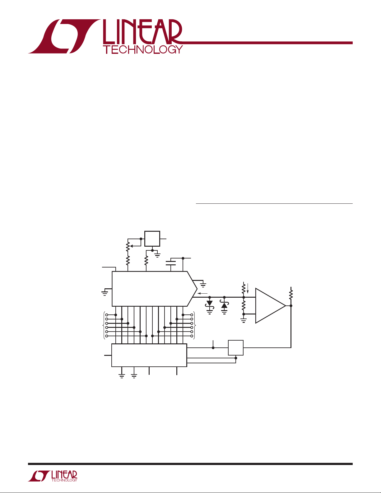
Figure 1 shows a simple 12-bit, 12µs SAR converter. Understanding this circuit’s performance limitations is useful
L, LT, LTC, LTM, Linear Technology and the Linear logo are registered trademarks of Linear
Technology Corporation. All other trademarks are the property of their respective owners.
–15V
19
DAC I
18
PARALLEL
OUTPUTS
SERIAL OUTPUT
*R2 AND R4 SHOULD TC TRACK
INPUT
0V TO 10V
R4*
2.49k
R6
820
7475
LATCH
I
2
+
LT1011A
3
–
5V
R5
1k
7
AN17 F01
Figure 1. Basic 12-Bit, 12μs Successive Approximation A→D Converter
an17f
AN17-1
Page 2
Application Note 17
in designing faster converters. Figure 2 shows waveforms
of operation. Trace A is the clock, which is applied to the
2504 IC successive approximation register (SAR), while
Trace B is the start pulse. On the rising edge of the start
pulse, the SAR-DAC combination begins to test each
bit, beginning with the MSB. This action is reflected in
conditions at the LT1011’s positive input (Trace C). This
waveform is seen to sequentially converge towards zero
as the SAR, DAC and comparator servo the node. After
the LSB has been converted the “conversion complete”
(CC) line (Trace D) goes high, signaling the end of the
sequence. The 7475 latch prevents the comparator from
responding to input noise or shifts after the conversion is
complete. It is reset at the next “conversion command”.
The major limitations on speed in this circuit are the DAC
and the comparator. Most bipolar DACs require 150ns to
200ns to settle for a worst-case (full-scale) step and the
comparator’s delay time must also be accounted for. The
clamp diodes limit overdrive, aiding comparator response.
Additionally, the 820 resistor to ground shunts the DACs
output capacitance, helping the comparator-DAC node
settle more quickly. The shunt degrades the voltage perLSB available to the comparator, but the LT1011’s high
gain makes up for this.
In general, this is a fairly typical 12-bit SAR converter with
good speed and low cost. To get higher conversion speed
requires more sophisticated circuitry.
Figure 3 shows a circuit, which uses a clock modulation
scheme to decrease conversion time. The A→D is identical
to Figure 1’s circuit, but the clock terminal (CP) is driven
by a 2-speed oscillator. Figure 4 shows operating details.
A convert command pulse (Trace A) initiates the SAR routine. Simultaneously, the 7474 flip-flop’s Q output is set
high (Trace C), biasing Q1. This causes the 47pF capacitor
to be paralleled with the 33pF unit. These capacitors are
part of the timing network of C1, which is configured as
an oscillator. C1’s output pulses (Trace B) drive the SAR’s
clock terminal (CP in the schematic). After the third MSB
has been converted, the flip-flop is reset (Trace C). Q1
goes off and the clock oscillator (Trace B) speeds up. The
increase in clock speed results in less dwell time per bit
at the DAC-comparator junction (Trace D), allowing faster
total conversion time. Trace E, the conversion complete
pulse (CC), drops low 7.5µs after the conversion started.
This clock modulation approach buys significantly improved speed, but does nothing to get around the comparator’s contribution to delay. Minimizing comparator delay
would seem to be as simple as using a faster device. At
the 8-bit or even 10-bit level this usually works, but 12-bit
performance raises problems. Replacing the LT1011, a
150ns device, with a 10ns LT1016 increases speed, but
decreases available gain. The LT1011 has a minimum
gain of 200,000. The LT1016’s high speed sacrifices gain.
AN17-2
A = 5V/DIV
B = 5V/DIV
C = 200mV/DIV
D = 5V/DIV
HORIZ = 2µs/DIV
Figure 2. 12μs A→D Waveforms
AN17 F02
an17f
Page 3

Application Note 17
Minimum gain for this device is 1400. For a 10V full-scale
A→D, the LSB size is given by:
4096 steps
10V
= 2.44mV/LSB
PARALLEL
OUTPUTS
15V
5V
R1
1k
FULL-SCALE
TRIM
R2*
6.49k
13
12 11 10 9 876 5 432
4 5 6 7 8 9 161718192021
24
12
LT1021
7V
R3
6.98k
0.001µF
6012 12-BIT
D/A CONVERTER
AM2504
SAR REGISTER
SE
15V
To switch a full TTL output level with one-half LSB overdrive
(1.22mV), the comparator must have a minimum gain of:
5V
= 4,098
DAC I
PARALLEL
OUTPUTS
SERIAL OUTPUT
INPUT
0V TO 10V
R4*
2.49k
R6
820
7475
LATCH
I
2
3
+
C2
LT1011A
–
5V
R5
1k
7
AN17 F03
16151420
CP
1.22mV
17
1
D
CC
S
–15V
19
18
7474
CONVERT
COMMAND
1k
1k
5V
47pF
4.7k
QQ
PRESETCLR
15k
–5V
Q1
2N2369
33pF
+
LT1016
–
1k
C1
NC
6.8k
Figure 3. 7.5μs A→D Using a 2-Speed Clock
A = 5V/DIV
B = 10V/DIV
C = 10V/DIV
D = 200mV/DIV
E = 5V/DIV
HORIZ = 1µs/DIV
AN17 F04
Figure 4. Figure 3’s Waveforms
an17f
AN17-3
Page 4

Application Note 17
This figure clearly means the comparator cannot do the job
without some help. The input signal reduction caused by
the shunt resistor at the DAC output worsens the problem.
Finally, the comparator’s speed degrades for such low
level overdrives.
The solution to the aforementioned difficulties is to place
a gain stage ahead of the comparator. While the gain stage
adds some delay, it also increases gain, providing the
needed overdrive to the comparator.
Figure 5 shows a simple pre-amplifier. This pre-ampcomparator combination gives adequate gain and an
overall response time of 40ns to 50ns. A1 is set up as a
Schottky bounded amplifier. The bound diodes prevent A1
from saturating due to excessive summing point overdrive,
aiding response time. The 10pF capacitor, a typical value,
HP5082-2810
compensates DAC output capacitance and is selected for
best amplifier damping. The 10k feedback resistor, also
typical, is chosen for best gain-bandwidth performance.
Voltage gains of 4 to 10 are common. Figure6 shows performance. Trace A, a test input pulse, causes A1’s output
(Trace B) to slew through zero (screen center horizontal
line). When A1 crosses zero, C1’s input biases negative
and it responds (C1’s output is Trace C) 10ns later with
a TTL output.
A simple circuit like this results in faster comparisons.
Substituted for the LT1011 in Figure 3’s circuit, it permits
conversion times in the 3s to 5s range. Further reduction in conversion time is possible with a faster discrete
preamplifier.
10pF
V
IN
DAC
R
DAC I
SHUNT
I
IN
R
–
LT318A
+
10k
A1
–
LT1016
+
Figure 5. Simple Pre-Amplifier for the Comparator
A = 0.1V/DIV
B = 1V/DIV
C = 5V/DIV
HORIZ = 20ns/DIV
C1
L
OUTPUT
AN17 F05
AN17 F06
AN17-4
Figure 6. Pre-Amplified Comparator Waveforms
an17f
Page 5

Application Note 17
Figure 7 shows a very fast pre-amplifier built with GHz
range transistors. This cascoded differential amplifier is
placed ahead of C1, an LT1016. Q4 and Q5 provide bias
current compensation for Q1’s base current. Figure 8
0.01µF
150
V
IN
1k
* = 1% FILM RESISTOR
Q1–Q5 = RCA CA3127 ARRAY
FROM DAC
150k
R
DAC I
5V
I
IN
1k
150k15k
Q4
Q5
shows results for a test input signal (Trace A). C1’s output
(TraceB) switches in 15ns to 20ns. About 10ns of this delay
is due to C1, with the pre-amplifier contributing the rest.
5V
2.5k
620*620*
–
Q3
Q1
C1
LT1016
+
1N4148
Q2
AN17 F07
27k
–15V
OUTPUT
Figure 7. Fast Pre-Amplifier Comparator
A = 10mV/DIV
B = 2V/DIV
HORIZ = 10ns/DIV
Figure 8. Fast Pre-Amplifier Comparator Waveforms
AN17 F08
an17f
AN17-5
Page 6

Application Note 17
Figure 9 shows the discrete pre-amplifier used in a very
fast 12-bit SAR converter. The design utilizes a variety of
techniques to attain extremely high speed. Primary speed
enhancing features include a closed loop clock control
10V
LT1021
5V
9
74121
IN B
34 5
1000pF –5V
SD210
6
Q
7
15V
1k
PARALLEL
DIGITAL DATA
–15V
OUTPUT
10V
0.01µF
5V
16
24
13
10k**
COMP
V
CLK
V
R+VR–
+
10k
GND
12 1
GND
AM6012
Q6
AM2504
I
O
15V –15V
SE
14 3
method and active summing node clamping. The circuit
achieves a full 12-bit conversion in 1.8µs, about the practical limit with off-the-shelf components.
5V
0.01µF
150
V
IN
0V TO 10V
201915 1314
17
+
V
V
CC
2.5k**
–
18
I
O
LSBMSB
11
D
150k
1k
1k
5V
150k
15k
Q4
Q5
620*
Q3
Q1
2.5k
–15V
Q2
27k
620*
1/4 74S00
5V
–5V
1
–
LT1016
+
7
5
8
C1
NC
9
6
4
3
Q1-Q5 = RCA CA3127 ARRAY
= 1N4148
= HP5082-2810
*1% FILM RESISTOR
**PRECISION 0.01%; VISHAY S-102
5V
1k
0.1µF 10
10
1k
–5V
0.1µF
5V
1
4
3
3
4
–
LT1016
+
–5V
5V
+
LT1016
–
–5V
6
8
C3
5
1
C2
5
NC
9
7
1/4 74S08
6
8
PRS
9
NC
7
1/2 74S74
RST
Figure 9. 12-Bit 1.8μs SAR A→D
1/4 74S00
Q
CLOCK
D
1/2 74S74
CLK
1/6 74S04
7.4MHz
PRS
1/6 74S04
Q
1/4 74S08
AN17 F09
STATUS
CONVERT
COMMAND
AN17-6
an17f
Page 7

Application Note 17
The design is similar in concept to Figure 3, except that
the fast pre-amplifier replaces the LT1011. Additionally, the
clock speed change is implemented with the digital logic
shown. Unlike before, the clock rate is accelerated after
the fifth MSB is converted. During conversion of the upper
four bits, the clock rate is controlled by a closed loop to
maximize overall speed. The loop monitors conditions at
the DAC-comparator summing node. If the node is outside ±50mV, the SAR is clocked at the maximum rate. For
node responses inside ±50mV, the clock rate is retarded,
giving adequate time for settling. The clock loop speeds
conversion by not waiting for bits which aren’t going to
settle within ±50mV. C2 and C3 form a high speed window
comparator, which delivers summing node information in
digital form to the clock logic.
Figure 10 shows the effects of the closed loop clocking
scheme. Trace A is the convert command. Trace B is the
gated output of the C2-C3 window comparator. Trace B’s
state controls the clock line, which is Trace C. Trace D is
the summing point, and the dwell time-per-bit is controlled
by the window comparator’s decision. Beyond the fifth
bit, the SAR’s Q6 line instructs the clock logic to run at
maximum speed. As described to this point, the circuit
achieves a 1.9µs conversion time.
If the 74121 one-shot and associated circuitry are included,
conversion time is reduced to 1.8µs. These components
form an active clamp at the DAC-comparator summing
node. Each time the SAR clock is pulsed (Trace A, Figure11),
the 74121 puts out a 30ns FET gate pulse (Trace B). The
FET comes on, shunting the summing node (Trace C) to
ground. The FET’s low on-resistance aids DAC settling by
discharging the DACs 30pF output capacitance for 30ns.
The summing node (Trace C) is reset to zero by this action
at each SAR-directed step. When the one shot times out,
the node settles to its final value. This active clamping
results in about a 10ns-per-bit time savings.
The circuit’s 1.8µs conversion time is very close to what
is practically achievable for a 12-bit SAR A→D converter.
The special techniques used result in an effective DAC
settling time of about 100ns per bit. Comparator-pre-amp
delay is about 20ns per bit and SAR chip delays are in the
25ns per bit range. Adding these together gives:
100ns + 20ns + 25ns • 12 = 1.74µs.
The comparator and SAR delays, about 31% of the total,
are not easily reduced. A discrete Schottky SAR design
and a faster pre-amp can cut this figure somewhat, but
the DAC settling time, 69% of the total, remains. The effective 100ns/bit DAC settling time compares favorably
with published specifications for monolithic DACs, and is
not readily reducible. Beyond this speed, other conversion
methods are required.
A = 10V/DIV
B = 10V/DIV
C = 10V/DIV
D = 200µV/DIV
A = 10V/DIV
B = 20V/DIV
C = 50mV/DIV
HORIZ = 200ns/DIV
Figure 10. Figure 9’s Waveforms Figure 11. Figure 9’s Waveforms Using Active Clamping
Information furnished by Linear Technology Corporation is believed to be accurate and reliable.
However, no responsibility is assumed for its use. Linear Technology Corporation makes no representation that the interconnection of its circuits as described herein will not infringe on existing patent rights.
AN17 F10
HORIZ = 100ns/DIV
AN17 F11
AN17-7
an17f
Page 8

Application Note 17
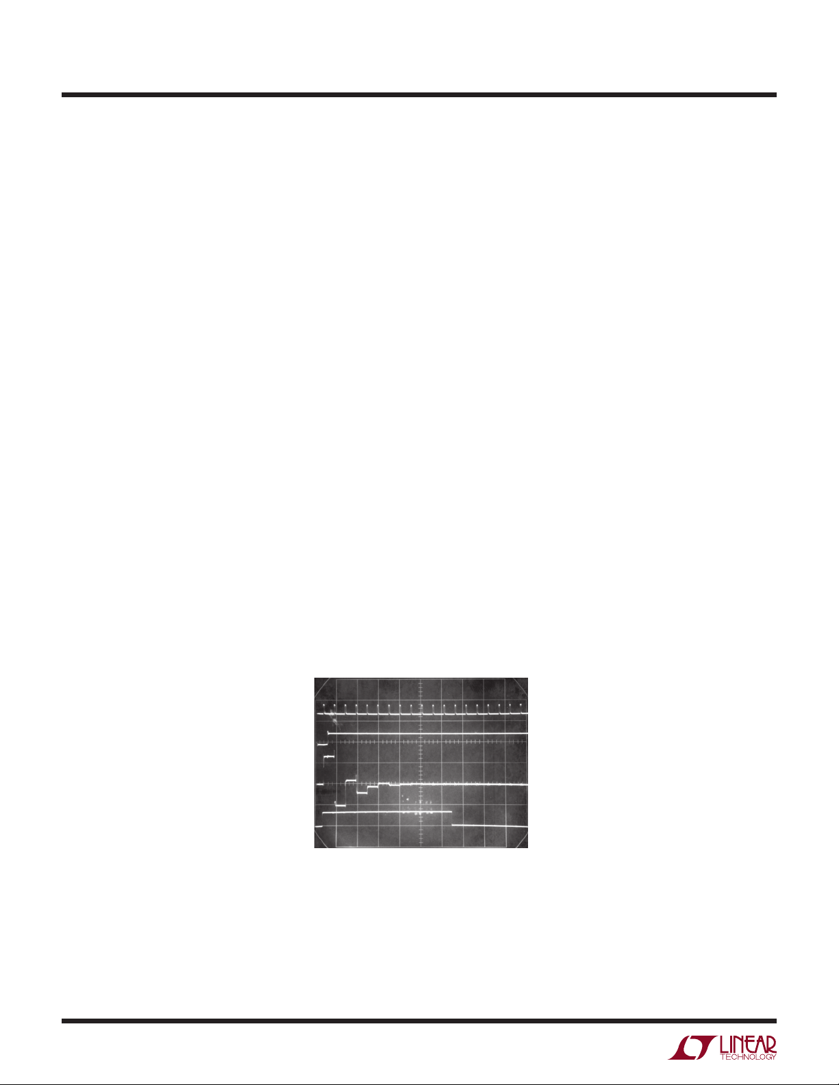
The Successive Approximation Technique
The successive approximation technique is probably as
old as the first crude weighing scale ever constructed. It
is most easily visualized when considering the operation
of a beam balance. The unknown weight, in one pan, is
determined by successive trails with standard weights
placed in the other pan. Overweight-underweight decisions are made by the balance as standard weights (and
combinations of them) are successively tried in a logical
sequence, which converges towards balancing the scale.
Successive approximation A→D converters start with
the MSB and proceed toward the LSB as each under-over
decision is made. The figure shows the summing node
response (Trace A) as the DAC, instructed by the clock
driven (Trace B) successive approximation register (SAR)
logic, tries different bit weights. The comparator’s decisions are also shown (Trace C). Note how the summing
point sequentially converges towards zero, the analog of
null in a beam balance.
Digital to Analog Converters in SAR Applications
Selecting a DAC for use in a SAR-based A→D requires
some thought. Most often, bipolar current mode DACs
are employed because of their higher speed. CMOS DACs
output capacitance, in the 100pF to 150pF range, causes
excessive summing node settling times. Monolithic bipolar
types, in the 30pF region, settle more quickly. Voltage
mode output DACs are almost never used because they
are not necessary to achieve summing action and they
are substantially slower than current output types.
Speed is often important, and since the DAC is the slowest
part of the converter, it should be carefully considered.
Settling time specifications for DACs are usually stated
for full-scale transitions. Smaller bit changes take less
VOLTAGE
INPUT
time, so some interpretation of the full-scale settling
time number can be made when considering the DAC’s
effective settling time-per-bit in an A→D application.
Unfortunately, the complex dynamics of DAC internals
prevent simple straight line calculations (e.g., 1 LSB will
not settle in one-half the time of full-scale for a 12-bit
unit). At moderate speeds, the simplest course is to allow
the specified full-scale settling time for each bit decision.
The conservative method will never get you into trouble,
but almost certainly guarantees slower than necessary
DAC performance. The best way to find out just how far
you can push the DACs settling time specification in a
SAR application in to consult the manufacturer. Additionally, it is worthwhile to actually measure the settling time
under conditions appropriate to the intended use (see LTC
Application Note 10, “Methods for Measuring Op Amp
Settling Time”, for circuits readily adaptable to DAC settling time measurements). The wide variety of DACs and
individual output termination requirements make obtainable results vary considerably. However, some guidelines
on what to expect are possible. For example, the popular
565A type, specified at 250ns full-scale settling time into
0, can achieve 110ns to 150ns effective settling timeper-bit in SAR applications with careful design. It is also
worth noting that the dynamics of DAC types can vary
considerably between manufacturers of what is nominally
the same part.
Speed is not the only concern. The DACs DC specifications
translate directly into A→D error terms. Linearity, drift,
accuracy and other DC terms contribute on a 1:1 basis
to the A→D’s error characteristics. One specification,
monotonicity, can contribute a particularly nasty term.
The effect of a non-monotonic DAC is an inability of the
A→D to produce some output codes (missing codes)
under any input condition.
SUCCESSIVE
APPROXIMATION LOGIC
REGISTER (SAR)
AN17-8
DAC
CLOCK
SUMMING
POINT
CURRENT
OUTPUT
I
COMPARATOR
I
AN17 F12
Basic SAR Circuit and Waveforms
Linear Technology Corporation
1630 McCarthy Blvd., Milpitas, CA 95035-7417
(408) 432-1900 ● FAX: (408) 434-0507
●
www.linear.com
A = 0.1V/DIV
B = 5V/DIV
C = 5V/DIV
HORIZ = 20µs/DIV
GP/IM 1285 10K • PRINTED IN USA
© LINEAR TECHNOLOGY CORPORATION 1985
AN17 F13
an17f
 Loading...