

Page 1
Application Note 16
Unique IC Buffer Enhances Op Amp Designs,
Tames Fast Amplifiers
Robert J. Widlar
August 1985
Abstract: A unity gain IC power buffer that uses NPN
output transistors while avoiding the usual problems of
quasi-complementary designs is described. Free of parasitic oscillations and stable with large capacitive loads, the
buffer has a 20MHz bandwidth, a 100V/μs slew and can
drive ±10V into a 75Ω load. Standby current is 5mA. A
number of applications using the buffer are detailed, and
it is shown that a buffer has many uses beyond driving
a heavy load.
Introduction
An output buffer can do much more than increase the
output swing of an op amp. It can also eliminate ringing
with large capacitive loads. Fast buffers can improve the
performance of high speed followers, integrators and
sample/hold circuits, while at the same time making them
much easier to work with.
Interest in buffers has been low because a reasonably
priced, high performance, general purpose part has not
been available. Ideally, a buffer should be fast, have no
crossover distortion and drive a lot of current with large
output swing. At the same time, the buffer should not eat
much power, drive all capacitive loads without stability
problems and cost about the same as the op amps it is
used with. Naturally, current limiting and thermal overload
protection would be nice.
These goals have been a dream for twenty years; but thanks
to some new IC design techniques, they have finally been
reached. A truly general purpose buffer has been made that
is faster than most op amps but not hard to use in slow
applications. It is manufactured using standard bipolar
processing, and die size is 50 × 82 mils.
The electrical characteristics of the buffer are summarized
in Table 1. Offset voltage and bias current win no medals;
but the buffer will usually be driven from an op amp output
and put within the feedback loop, virtually eliminating these
terms as errors. Loaded voltage gain is mostly determined
by the output resistance. Again, any error is much reduced
with the buffer inside a feedback loop.
Unloaded, the output swings within a volt of the positive
supply and almost to the negative rail. With ±150mA loading, this saturation voltage increases by 2.2V. Except for
output voltage swing, performance is little affected for a
total supply voltage between 4V and 40V. This means that
it can be powered by a single 5V logic supply or ±20V op
amp supplies.
Bandwidth and slew rate decrease somewhat with reduced
load resistance. The values given in Table 1 are for a 100Ω
in parallel with 100pF. The speed is quite impressive considering that quiescent current is but 5mA.
Table 1. Typical Performance of the Buffer at 25°C. Supply
Voltage Range is 4V to 40V
PARAMETER VALUE
Output Offset Voltage 70mV
Input Bias Current 75μA
Voltage Gain 0.999
Output Resistance 7Ω
Positive Saturation Voltage 0.9V
Negative Saturation Voltage 0.1V
Output Saturation Resistance 15Ω
Peak Output Current ±300mA
Bandwidth 22MHz
Slew Rate 100V/μs
Supply Current 5mA
L, LT, LTC, LTM, Linear Technology and the Linear logo are registered trademarks of Linear
Technology Corporation. All other trademarks are the property of their respective owners.
an16f
AN16-1
Page 2
Application Note 16
Design Concept
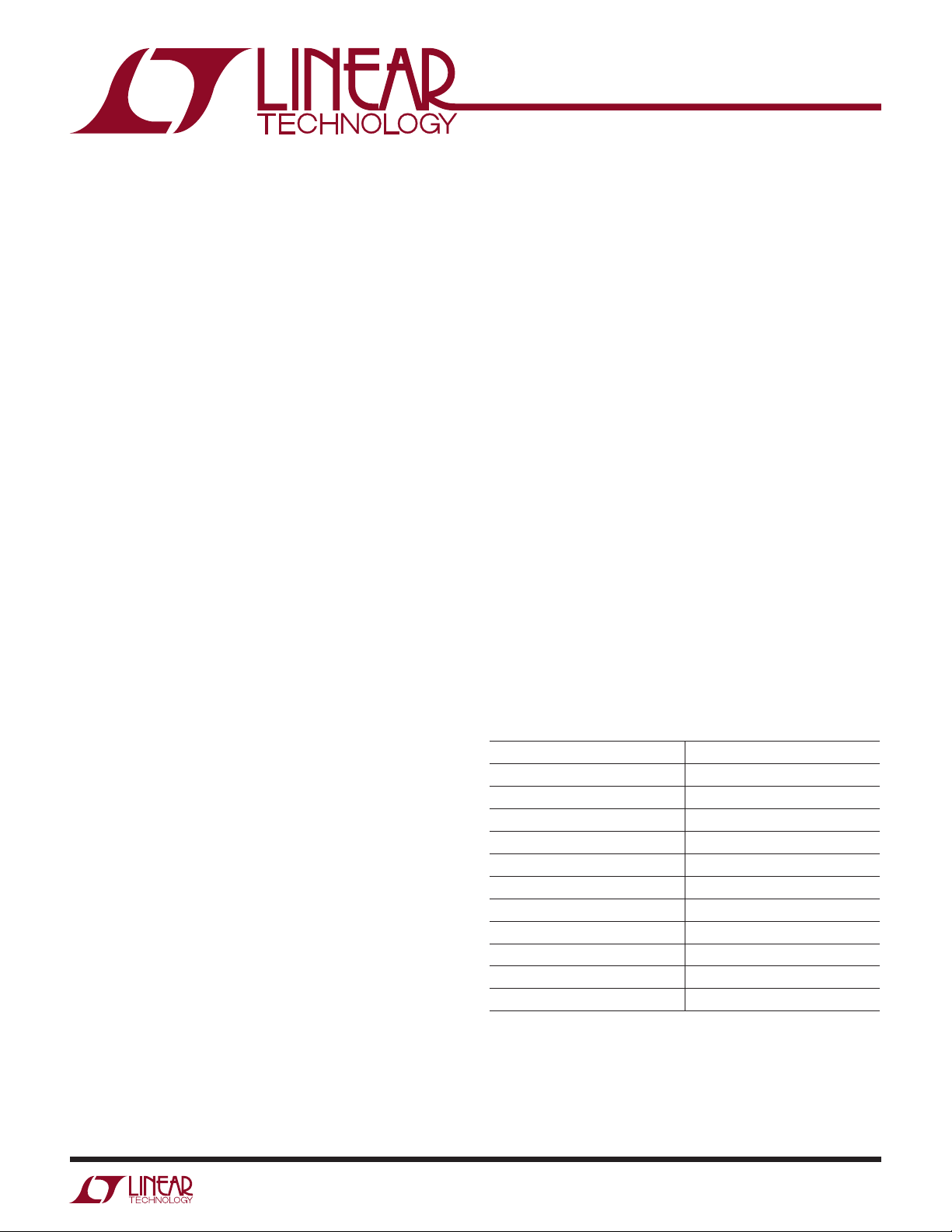
The functional schematic in Figure 1 describes the basic
elements of the buffer design. The op amp drives the
output sink transistor, Q30, such that the collector current of the output follower, Q29, never drops below the
quiescent value (determined by I
and the area ratio of
1
Q12 and Q28). As a result, the high frequency response
is essentially that of a simple follower even when Q30 is
supplying the load current. The internal feedback loop is
isolated from the effects of capacitive loading by a small
resistor in the output lead.
The scheme is not perfect in that the rate of rise of sink
current is noticeably less than for source current. This
can be mitigated by connecting a resistor between the
+
bias terminal and V
, raising quiescent current. A feature
of the final design is that the output resistance is largely
independent of the follower current, giving low output
resistance at low quiescent current. The output will swing
to the negative rail, which is particularly useful with singlesupply operation.
+
V
Q28Q12
BIAS
+
–
A1
I
C23
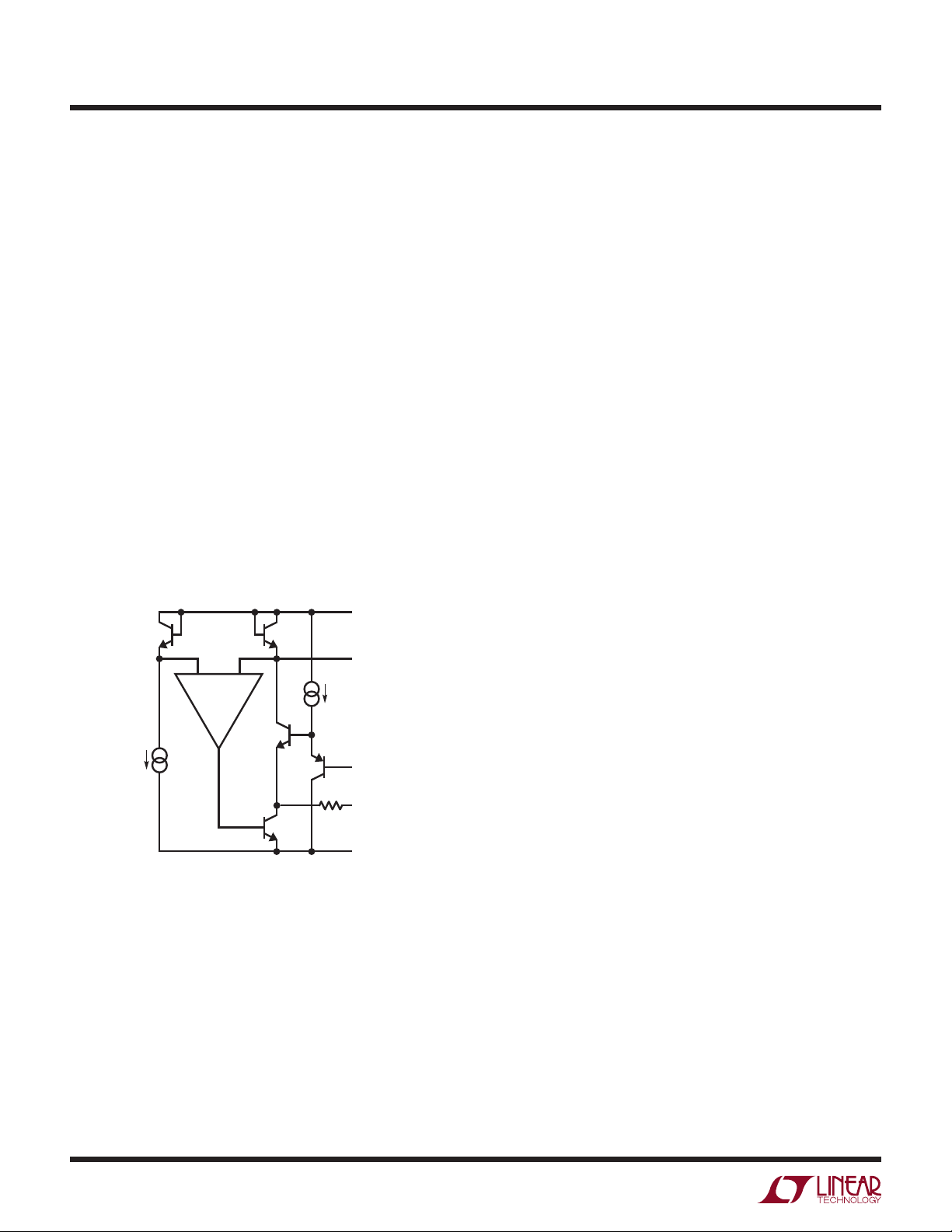
Basic Design
Figure 2 shows the essential details of the buffer design
using the concept in Figure 1 (for clarity, parts common
to simplified and developed schematics use the same
number). The op amp uses a common base PNP pair, Q10
and Q11, degenerated with R6 and R7 for an input stage.
The differential output is converted to single-ended by a
current mirror, Q13 and Q14; and this drives the output
sink transistor, Q30, through a follower, Q19.
A clamp, Q15, is included to insure that the output sink
transistor does not turn off completely. Its biasing circuitry
Q6 through Q9, is arranged such that the emitter current
of Q15 is about equal to the base current of Q19 with no
output load.
The control loop is stabilized with a feedforward capacitor,
C1. Above 2MHz, feedback is predominantly through the
capacitor. The break frequency is determined by C1 and R7
plus the emitter resistance of Q11. The loop is made stable
for capacitive and resonant loading by R23, which limits
the phase lag that can be induced at the emitter of Q29.
A resistor, R10, has been added to improve the negative
slew response. With a large negative transient, Q29 will
cut off. When this happens, R10 pulls stored charge from
Q28 and provides enough voltage swing to get Q30 from
its clamp level into conduction.
Q29
I
1
Figure 1. In the Buffer, Main Signal Path Is Through Followers
Q21 and Q29. Op Amp Keeps Q29 Turned on Even When Q30 Is
Supplying Load Current, So Response Is That of Followers
Q21
Q30
R23
AN16 F01
INPUT
OUTPUT
–
V
Start-up biasing is done with a collector FET, Q4. Once in
operation, the collector current of Q6 is added to the drain
current of Q4 to bias Q5. These currents plus the current
through Q9 and Q10 flow through Q12 to set the output
quiescent current (along with R10).
Follower Boost
The boost circuit in Figure 3 reduces the buffer standby
current by at least a factor of three while improving performance. It does this by increasing the effective current
gain of Q29 so that the current source current I
, can be
C23
drastically cut. Secondly, it can give under 0.5Ω follower
output resistance at less than 3mA bias, something that
normally takes over 40mA. Hard as it may be to believe,
the boost does not degrade the high frequency response
of the final design.
an16f
AN16-2
Page 3
Application Note 16
+
R23
7
AN16 F02
V
BIAS
OUTPUT
INPUT
–
V
R10
300
R7
R6
Q5
Q6
Q4
R4
4k
R5
1k
Q10
Q9
100μ
Q8
100μ
1k
100μ
1k
Q11
Q15
Q14Q7 Q13
R20
200
700μ
C1
60
Q19
R14
4k
Q28Q12
Q23
Q29
Q30
Q21
Figure 2. Implementation of the Buffer in Figure 1. Simple Op Amp Uses Common Base PNP Input Transistors (Q10 and Q11).
Control Loop Is Stabilized with Feedforward Capacitor (C1); and Clamp (Q15) Keeps Q30 from Turning Off Entirely
+
V
0.7mA
INPUT
I
C23
Q24
Q21
–
V
R19
200
Q25
R21
3k
Q29
I
Q
OUTPUT
AN16 F03
Figure 3. This Boost Circuit Raises Effective Current Gain and
Transconductance of the Output Transistor, Giving Low Standby
Current Along with Low Output Resistance
If R19 is removed (opened), circuit operation becomes
clearer. Output resistance is determined by Q24, with Q25
and Q29 providing current gain. If the current through R21
is larger than the base current of Q29, output resistance is
proportionately reduced. Without R21, output resistance
depends on Q29 bias, like a simple follower.
The purpose of R19 is to provide a direct AC path at high
frequencies and kill unneeded gain in the boost feedback
loop. If R21 is properly selected, voltage change across R19
with loading is less than 40mV, so a small value causes no
problems (increasing load does cause Q21 bias current to
increase). The quiescent drop across R19 is set by sizing
Q24, Q25 and Q29 geometries.
Charge Storage PNP
At high frequencies, a lateral PNP looks like a low impedance between the base and emitter because charge stored
between the emitter and subcollector (the PNP base) has a
capacitive effect. The input PNP, Q21, has been designed to
have more than 30 times the stored charge of a standard
lateral for a given emitter current. This stored charge
couples in the input to slew internal stray capacitances
and drive the output follower while the boost circuitry is
coming into action.
Stored charge can be maximized in a lateral PNP by using
large emitter area and wide base spacing. Dimensions of
several mils are practical; diffusion lengths are in the order
of 6 mils with good processing.
an16f
AN16-3
Page 4
Application Note 16
A sketch of a charge storage PNP is shown in Figure 4.
With the dimensions shown, current gains of 10 can be
obtained regularly. A sinker base contact is shown here
because a low resistance from the base terminal to the
area under the emitter is important.
The charge stored under the emitter is most effective in
obtaining a fast charge transfer from base to emitter with
minimum change of emitter base voltage. Using the notation in Figure 4, this charge varies as:
W
BAE
S
E
∝ XC–X
()
X
E
E
QE∝
where SE is the emitter periphery. With XC fixed, it can be
shown that Q
is maximized for XE = 0.5XC.
E
P+ COLLECTOR
W
B
2 MILS
X
E
4 MILS
X
C
W
B
2 MILS
As will be seen on the complete schematic, the isolationbase transistor is used as a bias diode for current sources
because of its high V
. One (Q28) is also used in the
BE
collector of the output follower because the behavior at
very high current densities is much better than a standard
transistor.
20
10
N+ EMITTER
)
–3
19
10
18
10
NET CONCENTRATION (cm
17
10
0
4 8 12 16
JUNCTION DEPTH (μm)
Figure 5. Impurity Profile of Isolation-Base Transistor. In
Contrast, Typical Standard NPN Has Peak Base Concentration
of 5 × 1016cm–3 and Base Width of 1μm
P+ ISOLATION
SUBCOLLECTOR
+
N
AN16 F05
+
N
AN16 F04
SINKER
BASE
CONTACT
N
–
BASE
0.4 MILS
+
SUBCOLLECTOR
N
Figure 4. Charge Storage PNP is Lateral Structure with Base and
Emitter Dimensions of Several Mils. As Above, Current Gains of
10 are Practical
Isolation-Base Transistor
Transistors can be made by substituting an isolation diffusion for the normal base diffusion. Figure 5 shows the
impurity profile of such a transistor. Base doping under
the emitter is three orders of magnitude higher than standard transistors, and the base extends all the way to the
subcollector. The measured current gains of 0.1 are not
lower than might be expected.
The emitter-base voltage of an isolation-base transistor is
about 120mV greater than a standard IC transistor when
operating at the same emitter current. Production variations in V
are much less than standard NPNs, probably
BE
because net base doping is little affected by anything but
the isolation doping.
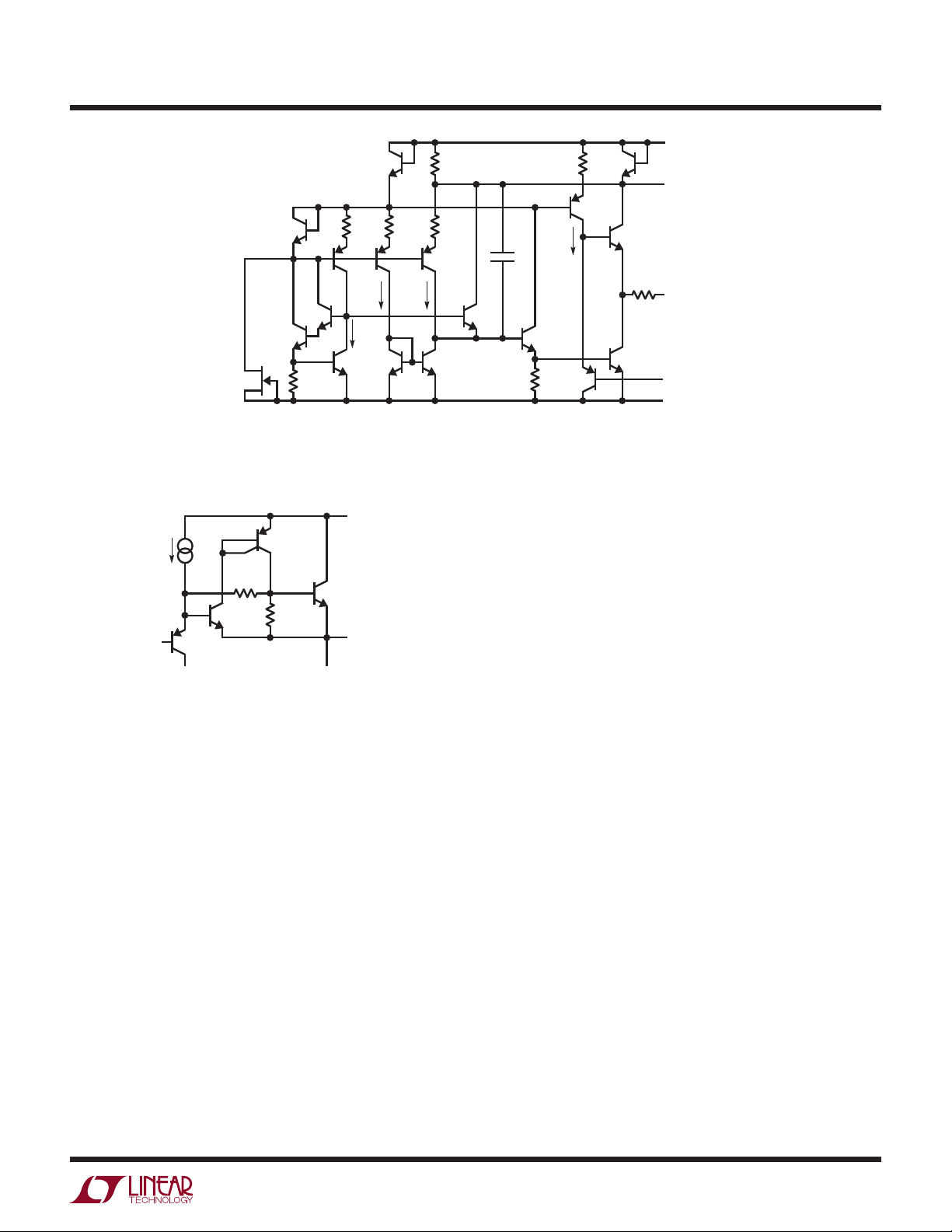
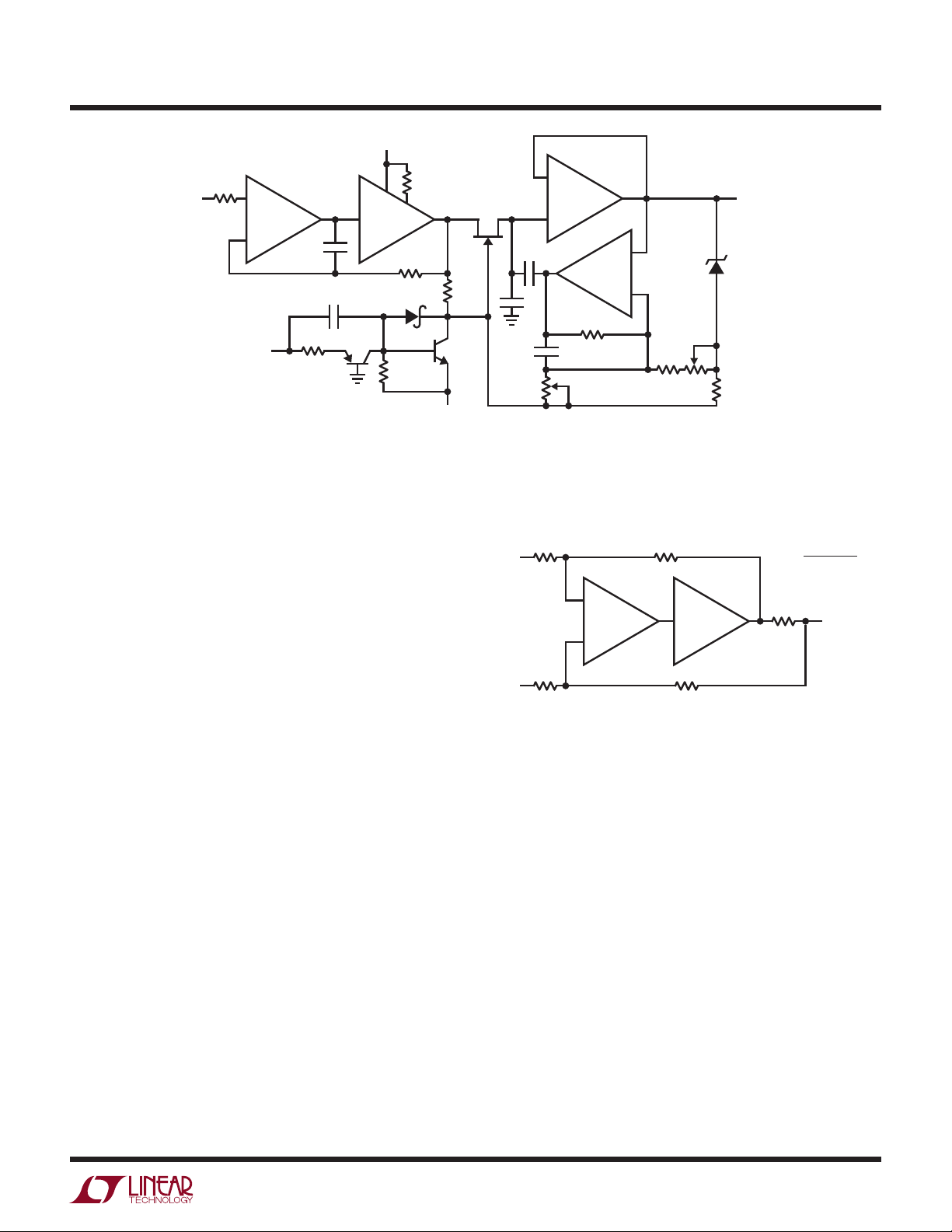
Complete Circuit
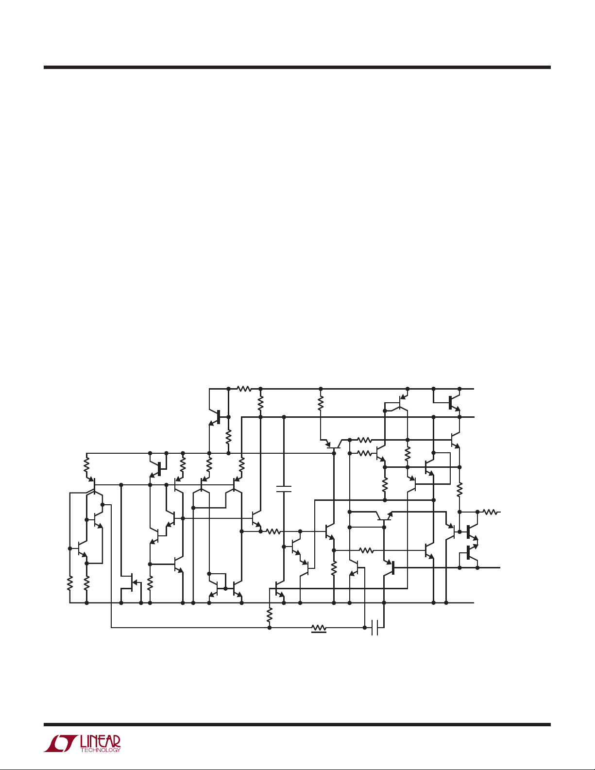
A complete schematic of the LT1010 buffer is given in
Figure 6. Component identification corresponds to the
simplified schematics. All details discussed thus far have
been integrated into the diagram.
Current limiting for the output follower is provided by
Q22 and Q31, which serve to clamp the voltage into the
follower boost circuitry when the voltage across R22
equals a diode drop.
Negative current limit is less conventional because putting
a sense resistor in the emitter of Q30 will seriously degrade
negative slew under load. Instead, the sense resistor, R17,
is in the collector. When the drop across it turns on Q27,
this transistor supplies current directly to the sink current
control amplifier, limiting sink current.
+
Should the output terminal rise above V
because of some
fault condition, Q27 can saturate, breaking the current limit
loop. Should this happen, Q26 (a lateral collector near Q27
base) takes over to control current by removing sink drive
through Q16. This reserve current limit oscillates, but in
a controlled fashion.
AN16-4
an16f
Page 5
Application Note 16
Clamp diodes, from the output to each supply, should
be used if the output can be driven beyond the supplies
by a high-current source. Unlike most ICs, the LT1010 is
designed so that ordinary junction diodes are effective
even when the IC is much hotter than the external diodes.
Current limit is backed up by thermal overload protection. The thermal sensor is Q1, with its base biased near
400mV. When Q1 gets hot enough to pull base drive off
Q2 (about 160°C), the collector of Q2 will rise, turning on
Q16 and Q20. These two transistors then shut down the
buffer. Including R2 generates hysteresis to control the
frequency of thermal limit oscillation.
Base drive to Q20 is limited by R15, a pinched base resistor. The value of this resistor varies as transistor h
fe
over temperature and in production, controlling the turn
off current near 2mA. An emitter into the isolation wall
capacitor, C2, keeps Q20 from turning on with fast signals
on its collector.
In current limit or thermal limit, excessive input-output
voltage might damage internal circuitry. To avoid this,
back-to-back isolation Zeners, Q32 and Q33, clamp the
input to the output. They are effective as long as the input
current is limited to about 40mA.
Other details include the negative saturation clamp, Q17
and Q18. This clamp allows the output to saturate within
100mV of the negative supply rail without increasing supply
current while recovering cleanly from saturation. The base
of Q17 is connected internally into Q30 to sense voltage
on the internal collector side of the saturation resistance
to insure optimum operation at high currents.
When sinking large currents, the base of Q19 loads the
control amplifier. This unbalances the control loop and
reduces the output follower bias current. To compensate
for this, the base current of Q30 is routed to the bias diode,
Q12, through Q19. A small resistor, R19, aids compensation. This action raises the bias to Q23 and is responsible
for increasing the input PNP bias current with sink current.
R9
15
Q18
R15
24k
R14
4k
R20
200
Q23
Q19
Q20
R19
200
R18
2k
R16
200
R17
C2
100
2
Q21
Q22
Q24
Q26
Q25
R21
3k
Q27
Q31
Q30
R10
Q11
Q14
300
R7
1k
C1
30
Q15
R12
1k
Q17
Q16
R13
4k
Q12
R8
15k
R6
R3
440
Q2
Q1
R2
R1
450
4k
Q5
Q6
Q4
R4
4k
R5
1k
1k
Q10Q9
Q8
Q7
Q13
Q28
Q29
R22
2
AN16 F06
+
V
BIAS
Q32
Q33
–
V
R23
5
OUTPUT
INPUT
Figure 6. Complete Schematic of the LT1010 Buffer. Component Identification Corresponds to Simplified Schematics.
The Isolation-Base Transistors Are Drawn with Heavy Base, as Is the Charge Storage PNP. Follower Drive Boost Has
Been Included Along with Negative Saturation Clamp (Q17 and Q18) and Protection Circuitry
an16f
AN16-5
Page 6
Application Note 16
Final details of the design are that the collectors of Q10
and Q11 are segmented so that only a fraction of the
emitter current is sent to the current mirror, with the rest
dumped to V-. This allows the transistors to be operated
A AC
D EB
at their f
peak without requiring large C1. Lastly, R8 has
T
been included to shape the temperature characteristics of
output stage quiescent current.
F
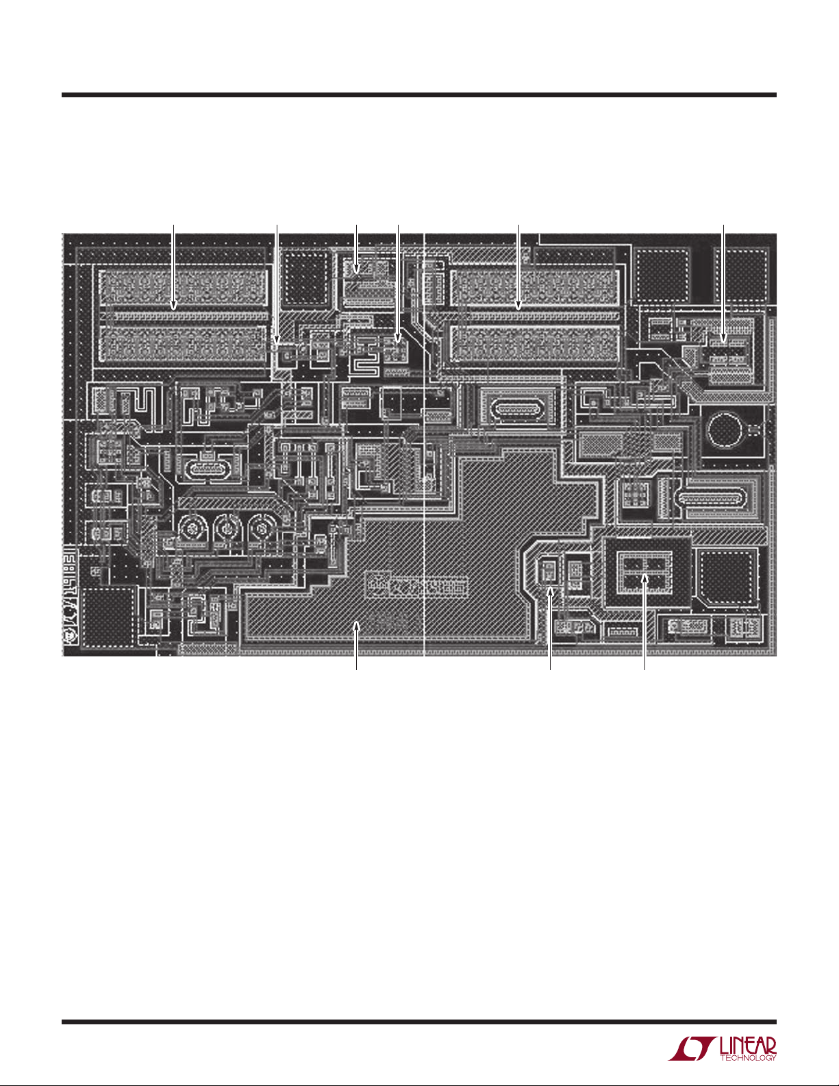
Figure 7. Plot of the LT1010. Die Size Is 50 × 82 Mils
A photomicrograph of the LT1010 die is shown in Figure7.
The features pointed out are identified below.
A) Output transistors were designed to maximize high
frequency performance, while obtaining some ballasting.
B) Clamp PNP base (Q17) is connected by subcollector
stripe to region furthest from Q30 collector contact to
isolate saturation resistance.
C) Output resistors are in floating tub so that IC tubs are
not forward biased when junction diodes clamp output
–
below V
.
AN16-6
G H
D) A high fT, 0.3 mil stripe, cross geometry is used for
the sink transistor driver (Q19).
E) Isolation-base transistor (Q28) carries the same 500mA
peak current as the output transistor but is much smaller.
F) MOS capacitor (C1) takes up considerable area.
G) Capacitance formed by diffusing emitter into isolation
wall takes advantage of unused area.
H) Charge storage PNP.
an16f
Page 7
Application Note 16
Buffer Performance
Table 1 in the Introduction summarizes the typical specifications of the LT1010 buffer. The IC is supplied in three
standard power packages: the solid kovar base TO-5
(TO-39), the steel TO-3, and the plastic TO-220. The bias
terminal is not available in the TO-39 package because it has
only four leads, compared to five for the other packages.
The thermal resistance for one output transistor, excluding
the package, is 20°C/W because it was kept as small as possible to enhance speed. This explains the junction-to-case
thermal resistance of 40°C/W for the TO-39 package and
25°C/W for the TO-3 and TO-220, again for one transistor.
With AC loads, both transistors will be conducting; if the
frequency is high enough, thermal resistance is reduced
by 10°C/W.
The operating case temperature range for the LT1010 is
–55°C to 125°C. The maximum junction temperature for
the internal power transistors is 150°C. A commercial
version, the LT1010C, is also available. It rated for 0°C
to 100°C case temperature with a maximum junction
temperature of 125°C.
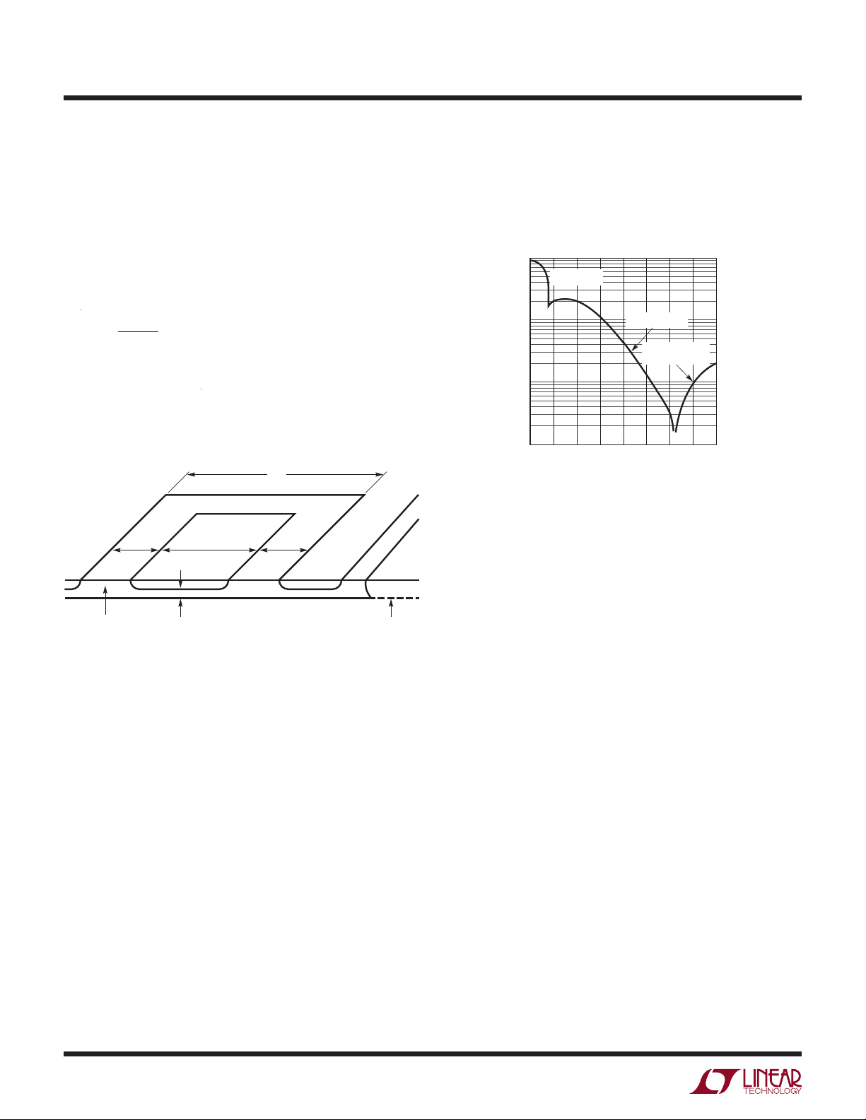
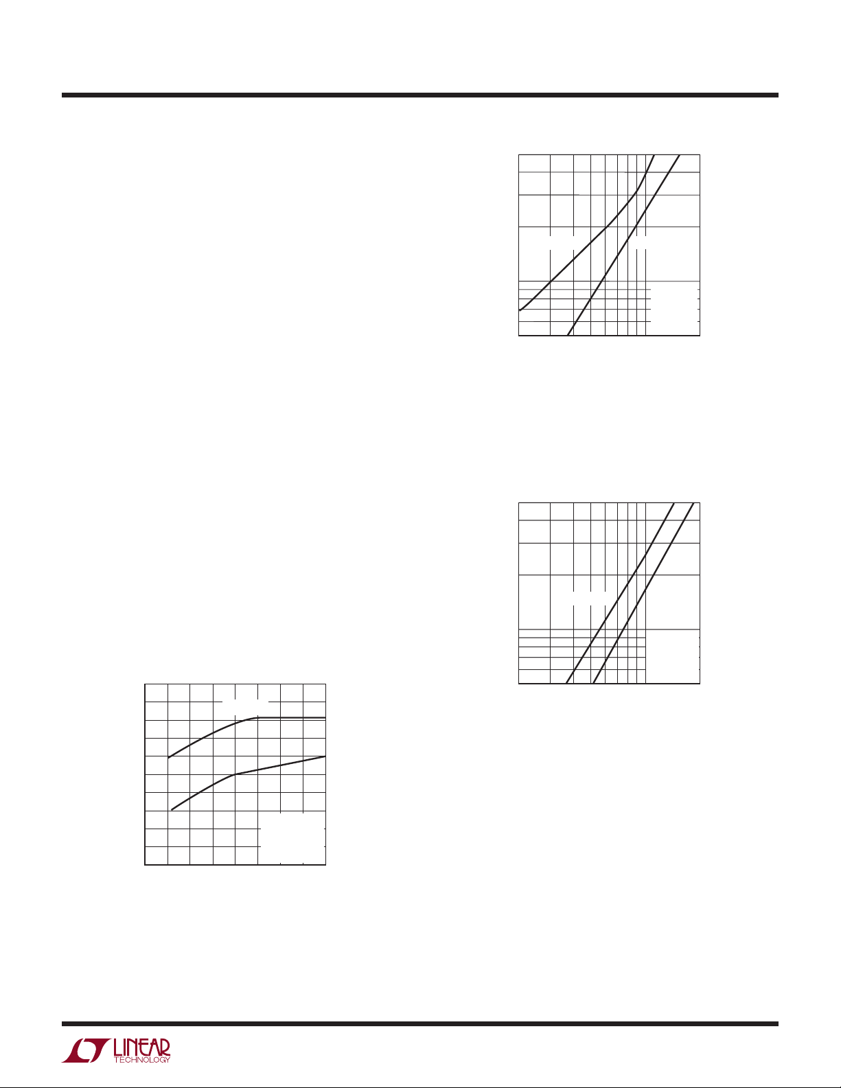
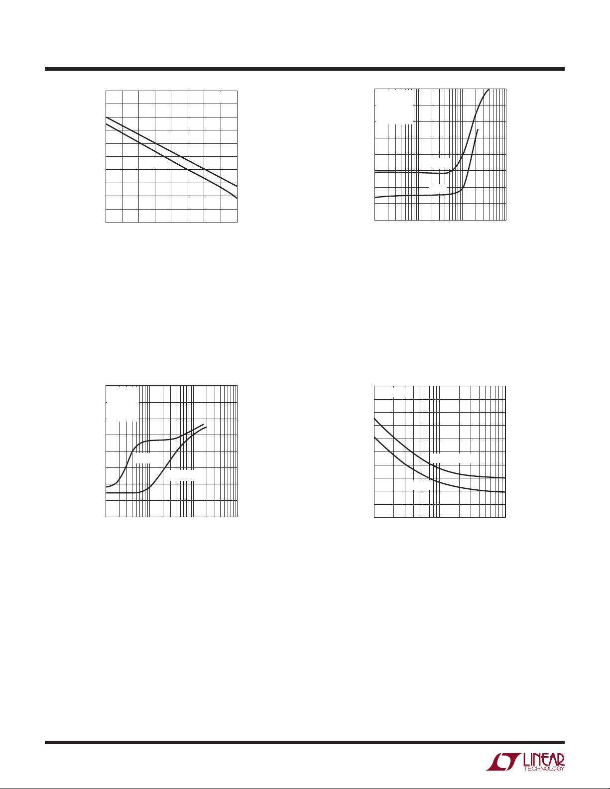
Phase Delay
50
20
RL = 50Ω 200Ω
10
PHASE LAG (DEGREES)
5
2
51020
FREQUENCY (MHz)
Figure 9. The Phase Delay Gives More Useful Information
About High Frequency Performance Than Bandwidth. This Is
a Plot of Phase Delay as a Function of Frequency with 50Ω
and 100Ω Loads. Capacitive Loading Is 100pF, and Quiescent
Current Is Not Boosted
50
CL = 100pF
= 50Ω
R
S
= 0
I
BIAS
= 25°C
T
J
AN16 F09
The following curves describe the buffer performance in
some detail. The fact that quiescent current boost (5mA
– 40mA) is not available on the TO-39 package should
be noted.
Bandwidth
50
40
30
20
FREQUENCY (MHz)
10
0
0
QUIESCENT CURRENT (mA)
Figure 8. The Dependence of Small Signal Bandwidth on Load
Resistance and Quiescent Current Boost Is Shown Here. The
100pF Capacitive Load That Is Specified Limits the Bandwidth
That Can Be Obtained with Boost and Light Loads
RL = 200Ω
50Ω
VIN = 100mV
CL = 100pF
A
V
= 25°C
T
J
10
20
= –3dB
30
PP
40
AN16 F08
20
RL = 50Ω
10
PHASE LAG (DEGREES)
5
2
FREQUENCY (MHz)
51020
200Ω
CL = 100pF
= 50Ω
R
S
= 20Ω
R
BIAS
= 25°C
T
J
AN16 F09
Figure 10. This Shows Reduction in Phase Lag with
Quiescent Current Boosted to 40mA (R
BIAS
= 20Ω)
an16f
AN16-7
Page 8
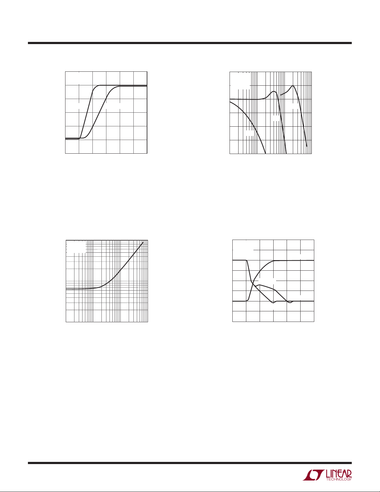
Application Note 16
Step Response Capacitive Loading
150
RL = 100Ω
= 25°C
T
J
100
50
INPUT OUTPUT
0
–50
VOLTAGE CHANGE (mV)
–100
–150
0
10 20
TIME (ns)
30
AN16 F11
Figure 11. The Small Signal Step Response with 100Ω Load
Shows a 2ns Output Delay. This Gives an Excess Phase Delay
of 15° at 20MHz, Explaining Why the –3dB Bandwidth Is
Greater Than the Frequency for 45° Phase Delay.
Output Impedance
100
I
= 0
BIAS
= 25°C
T
J
10
OUTPUT IMPEDANCE (Ω)
1.0
0.1
1 10 100
FREQUENCY (MHz)
AN16 F12
10
RS = 50Ω
= 0
I
BIAS
= 25°C
T
J
0
100pF
3nF
–10
VOLTAGE GAIN (dB)
–20
0.1
0.1μF
1 10 100
FREQUENCY (MHz)
AN16 F13
Figure 13. These Frequency Response Plots, with Capacitive
Load Only, Show That Nothing Unusual Happens as Load
Capacitance Is Varied Over a Wide Range. Minor Peaking Is
Reduced with Quiescent Current Boost
Slew Response
20
VS = ±15V
= 100Ω
R
L
15
= 25°C
T
J
f ≤ 1MHz
10
5
0
–5
OUTPUT VOLTAGE (V)
–10
–15
–20
–80
0
I
= 0
BIAS
R
= 20Ω
BIAS
50 150
100 200
TIME (ns)
POSITIVE
NEGATIVE
250
AN16 F14
Figure 12. The Unloaded Small Signal Output Impedance Stays
Down to 1MHz, Indicating the Frequency Limit of the Follower
Boost Circuitry
AN16-8
Figure 14. The Negative Slew Delay Is Reduced by Using
Quiescent Current Boost (40mA). Positive Slew Is Not
Affected by Boost.
an16f
Page 9

Application Note 16
400
VS = ±15V
≥ –10V
0V ≥ V
IN
300
200
SLEW RATE (V/μs)
100
0
0
RL = 200Ω
100Ω
50Ω
10
QUIESCENT CURRENT (mA)
20
30
40
AN16 F15
Figure 15. The Worst-Case Slew Response, Going from
0V to –10V, Is Plotted Here. It Is Clear That Substantial
Improvement Can be Made with Quiescent Current Boost
80
VS = ±15V
= ±10V
V
IN
= 0
I
L
= 25°C
T
C
60
40
SUPPLY CURRENT (mA)
20
0
0
2
1
FREQUENCY (MHz)
5
4
3
AN16 F17
Figure 17. The No Load Supply Current Increases Above 1MHz
Under Large Signal Conditions. This Is a Quiescent Current
Boost Caused by Charging of Internal Capacitances. It Does
Give Very Good Power Bandwidth Even with Load, Although the
Excess Dissipation May Cause the IC to Go into Power Limit
Input Offset Voltage
15
10
5
0
–5
OUTPUT VOLTAGE (V)
–10
–15
–1
0123
TIME (μs)
VS = ±15V
= 100Ω
R
L
= 0
I
BIAS
AN16 F16
4
Figure 16. This 500ns Slew Residue Is Caused by Recovery
of the Follower Boost Circuitry. For Positive Outputs, the
Boost Circuit Is Hit Hard by the Input Through the Charge
Storage PNP. For Negative Outputs, it Is Hit by the Leading
Edge Overshoot on the Output. Recovery Is from a Positive
Boost Overshoot in Both Cases.
200
VIN = 0V
150
V+ = 38V
–
= –2V
100
OFFSET VOLTAGE (mV)
50
0
–50
V
V+ = 2V
–
= –38V
V
0
50
TEMPERATURE (°C)
100
150
AN16 F18
Figure 18. The Offset Voltage is Determined by Matching
Between the Output Follower and the Input PNP. The Charge
Storage PNP on the Input Is Run at High Injection Levels to
Maximize Stored Charge. Therefore, the High Offset Voltage
Drift Shown Here Is No Surprise. The Offset Voltage Change
with Supply Voltage Shown in the Figure Is Mostly Positive
Supply Sensitivity. Changing the Negative Supply by 35V
Shifts Offset by 5mV
an16f
AN16-9
Page 10

Application Note 16
Input Bias Current Voltage Gain
200
VIN = 0V
150
V+ = 38V
–
= –2V
V
100
BIAS CURRENT (μA)
50
0
–50
0
V+ = 2V
–
= –38V
V
50
TEMPERATURE (°C)
100
150
AN16 F19
Figure 19. The Increase in Bias Current with Temperature
Reflects the Current Gain Characteristics of the Charge
Storage PNP. Sensitivity of Bias Current to Supply Voltage
Is About Three Times Greater on Positive Supply
200
150
TJ = 125°C
VS = ±15V
= 75Ω
R
L
1.000
I
= 0
OUT
VS = 40V
0.999
VS = 4.5V
GAIN (V/V)
0.998
0.997
–50
050
TEMPERATURE (°C)
100
150
AN16 F21
Figure 21. The Unloaded Voltage Gain Is High Enough to Be
Ignored in Most Any Application. In Practice, Gain Will Be
Determined by the Load Working Against the Output Resistance
Output Resistance
12
I
≤ 150mA
OUT
10
8
100
BIAS CURRENT (μA)
50
0
–100
–150
25°C
–55°C
–50 50
0 100
OUTPUT CURRENT (mA)
150
AN16 F20
Figure 20. The Change in Input Bias Current with Load Current
Is Not Excessive, but it Shows That the Follower Is Not Designed
for Working with High Source Resistances. For Positive Output
Current, Increase Is Caused by Follower Boost. For Negative
Output, It Results from Sink Transistor Base Current Increasing
Bias to the Input PNP Current Source
6
4
OUTPUT RESISTANCE (Ω)
2
0
–50
050
TEMPERATURE (°C)
100
150
AN16 F22
Figure 22. The Output Resistance Is Essentially Independent of
DC Output Loading. The Temperature Sensitivity Is Shown Here
an16f
AN16-10
Page 11

Output Noise Voltage
Application Note 16
200
TJ = 25°C
150
100
50
NOISE VOLTAGE (nV/√Hz)
0
10
RS = 1kΩ
RS = 50Ω
100 1k 10k
FREQUENCY (Hz)
AN16 F23
Figure 23. The Noise Performance of a Buffer Is of Small
Concern Unless it Is Grossly Bad. This Plot Shows That the
Buffer Noise Is Low by Comparison to the Excess Output
Noise of Op Amps
Saturation Voltage
4
3
IL = 150mA
4
3
2
1
SATURATION VOLTAGE (V)
0
–50
IL = –150mA
–50mA
–5mA
0
50
TEMPERATURE (°C)
100
150
AN16 F25
Figure 25. This Curve Gives the Negative Saturation Voltage.
Unloaded Saturation Voltage Is <0.1V, Again Increasing Linearly
with Current. The Saturation Characteristics Are Negligibly
Affected by Supply Voltage and Are Used to Determine Output
Swing Under Load
Supply Current
7
VIN = 0
= 0
I
OUT
= 0
I
BIAS
6
TJ = –55°C
2
1
SATURATION VOLTAGE (V)
0
–50
50mA
5mA
0
50
TEMPERATURE (°C)
100
150
AN16 F24
Figure 24. The Positive Saturation Voltage (Referred to the
Positive Supply) Is Plotted Here as a Function of Temperature.
Unloaded Saturation Voltage Is 0.9V, with the Saturation Voltage
Increasing Linearly with Current to 150mA
5
SUPPLY CURRENT (mA)
4
3
0
TOTAL SUPPLY VOLTAGE (V)
25°C
125°C
10
20
30
40
AN16 F26
Figure 26. Supply Current Is Not Greatly Affected by Supply
Voltage, as Shown in This Expanded-Scale Plot. This Accounts
for the 4V to 40V Supply Range with Unchanged Specifications
an16f
AN16-11
Page 12
Application Note 16
1.0
0.9
R
0.8
0.7
0.6
BIAS TERMINAL VOLTAGE (V)
0.5
–50
BIAS
20Ω
0
TEMPERATURE (°C)
= 100Ω
50
VS = ±20V
100
150
AN16 F27
Figure 27. The Quiescent Current Boost Is Determined by
the Bias Terminal Voltage Across an External Resistor. This
Expanded-Scale Plot Shows the Change in Bias Terminal
Voltage with Temperature. The Voltage Increases Less Than
20mV as the Total Supply Voltage Is Raised from 4.5V to 40V
Total Harmonic Distortion
0.8
I
= 0
BIAS
= ±15V
V
S
= ±10V
V
OUT
= 25°C
T
C
0.6
0.4
0.2
HARMONIC DISTORTION (%)
0
1
RL = 50Ω
100Ω
10 100 1000
FREQUENCY (kHz)
AN16 F29
Figure 29. Distortion Is Low to 100kHz, Even without
Quiescent Current Boost. The Influence of Load
Resistance Is Indicated Here
Maximum Power
0.4
RL = 50Ω
f = 10kHz
= ±15V
V
S
= 25°C
T
C
0.3
0.2
0.1
HARMONIC DISTORTION (%)
0
0.1
I
= 0
BIAS
R
= 50Ω
BIAS
1 10 100
OUTPUT VOLTAGE (VPP)
AN16 F28
Figure 28. The Buffer Distortion Is Not High, Even When
it Is Outside a Feedback Loop, as Shown Here. The
Reduced-Distortion Curve Is for 20mA Supply Current
10
TC = 85°C
8
6
4
PEAK POWER (W)
2
0
1
TO-3, TO-220
TO-39
10 100
PULSE WIDTH (ms)
AN16 F30
Figure 30. These Curves Indicate the Peak Power Capability of
One Output Transistor for T
= 85°C. With AC Loading, Power Is
C
Divided Between the Two Output Transistors. This Can Reduce
Thermal Resistance to 30°C/W for the TO-39 and 15°C/W for the
TO-3, as Long as the Frequency Is High Enough That the Peak
Rating of Neither Transistor Is Exceeded
AN16-12
an16f
Page 13

Application Note 16
Short Circuit Characteristics Isolating Capacitive Loads
0.5
0.4
0.3
0.2
OUTPUT CURRENT (A)
0.1
0
–50
SOURCE
0
TEMPERATURE (°C)
SINK
50
VS = ±15V
V
OUT
100
= 0
150
AN16 F31
Figure 31. The Output Short Circuit Current Is Plotted Here as
a Function of Temperature. Above 160°C it Falls Off Sharply
Because of Thermal Limit. The Peak Output Current Is Equal to
the Short Circuit Current; with Capacitive Loads Greater Than
1nF, Current Limiting Can Reduce Slew Rate
50
VS = ±15V
= 0
V
OUT
= 25°C
T
J
25
0
INPUT CURRENT (mA)
–25
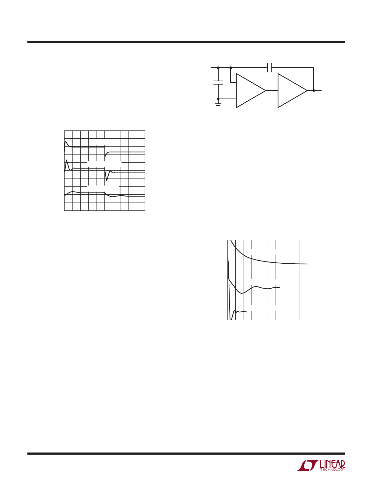
The buffered follower in Figure 33a shows the recommended method of isolating capacitive loads. At lower
frequencies, the buffer is within the feedback loop so that
offset voltage and gain errors are negligible. At higher frequencies (above 80kHz here) op amp feedback is through
C1 so that phase shift from the load capacitance acting
against the buffer output impedance does not cause
instability.
The initial step response is the same as if the buffer were
outside the feedback loop; the gain error of the buffer is
then corrected by the op amp with a time constant determined by R1C1. This is shown in Figure 33b.
With small load capacitors, the bandwidth is determined
by the slower of the two amplifiers. The op amp and the
buffer in Figure 33 give a bandwidth near 15MHz. This is
reduced for capacitive loads greater than 1nF (determined
by the output impedance of the buffer).
Feedback-loop stability with large capacitive loads is determined by the ratio of the feedback time constant (R1C1) to
that of the buffer output resistance and load capacitance
(R
where R
). A stability factor, m, can be expressed as
OUTCL
R1C1
m =
R
C
L
OUT
is the buffer output resistance.
OUT
R1
2k
–50
–15
–10
–5
INPUT VOLTAGE (V)
5
010
15
AN16 F32
Figure 32. The Input Characteristics, with the Output Shorted,
Are Plotted Here. The Input Is Clamped to the Output to Protect
Internal Circuitry. Therefore, it Is Necessary to Externally
Limit Input Current. The Output-Current Limit of IC Op Amps Is
Adequate Protection
m =
R1C1
R
OUTCL
C1
1μF
A2
LT1010
C
AN16 F33
V
OUT
L
–
LT118A
+
A1
R2
2k
V
IN
(33a) Connection Diagram
)V
Y
V
OUT
tq
)V =
Y
CL = 0
R
OUT
R
= R1C1
V
OUT
L
(33b) Step Response
Figure 33. Capacitive Loading on This Buffered Follower
Reduces Bandwidth Without Causing Ringing. Step Response
with No Capacitive Load Has Residue as Shown Here
an16f
AN16-13
Page 14

Application Note 16
IL = 0 m = 10
m = 4 m = 2 m = 1
OUTPUT VOLTAGE (2.5V/DIVISION)
Figure 34. Large Signal Step Response (±5V) of the
Buffered Follower in Figure 33 for Indicated Loads
RL = 100Ω
TIME (10μs/DIVISION)
AN16 F34
With R1C1 as shown in Figure 33, any op amp with a
bandwidth greater than 200kHz will give the same results
on stability. Settling time, however, will be dominated by
the slew rate limitations of slow op amps.
Certain op amps, like the LM118, have back-to-back
protection diodes across the input terminals. With input
rise times in excess of the op amp slew rate, C1 can be
charged through these diodes, increasing settling time.
Including R2 in series with the input takes care of the
problem. Good supply bypass (22μF solid tantalum) should
be used because high peak currents are required to drive
load capacitors and supply transients can feed into the op
amp, increasing settling time.
The measured large signal step response for the circuit
in Figure 33a is given in Figure 34 for various loads. For
m ≥ 4 (C
For m < 1 (C
Figure 35. Measured Settling For Output Steps in Figure 34.
For Capacitive Loads Less Than 0.068μF (m = 4) Settling Is
Based on a 2μs Time Constant
≤ 0.068μF) there is overshoot but no ringing.
L
> 0.33μF) ringing becomes pronounced.
L
20
IL = 0
m = 4
AND 10
10
m = 2
0
VOLTAGE ERROR (mV)
–10
–20
0
RL = 100Ω
20
40
TIME (μs)
m = 1
60
100
80
AN16 F35
The settling time constant is determined by R1C1 for
m ≥ 4. Without capacitive loading, the initial error on the
output step is smaller, so time to settle is less. The settling
characteristics are shown in Figure 35.
The same load isolation technique is shown applied to
an inverting amplifier in Figure 36. The response differs
in that the output rise time and bandwidth are limited by
R1C1. This does reduce overshoot for m ≥ 4, as shown
in Figure37. For m < 4, response approaches that of the
follower.
R2
2k
V
IN
R1C1
R
OUTCL
C1
1μF
–
A1
LT118A
+
R3
1k
m =
(36a) Connection Diagram
Y
(36b) Step Response
Figure 36. With an Inverter, Bandwidth and Rise Time Are
Limited by R1CL. For m ≥ 4, Capacitive Loading Has Little
Effect on Bandwidth
tq
V
LT1010
OUT
R1
2k
A2
Y
= R1C1
CL = 0
C
AN16 F36
V
OUT
L
AN16-14
an16f
Page 15

5
0
–5
5
0
OUTPUT VOLTAGE (V)
–5
–20
CL = 0
CL = 0.068μF
m = 4
020
60 100 120
40 80
TIME (μs)
AN16 F37
Figure 37. Large Signal Pulse Response of the Inverter
in Figure 36.
Although the small signal bandwidth is reduced by C1,
considerable isolation can be obtained without reducing it
below the power bandwidth. Often, bandwidth reduction is
desirable to filter high frequency noise or unwanted signals.
An alternate method of isolating capacitive loads is to buffer
an inverter output with the follower shown in Figure 33.
Capacitive load isolation for non-inverting amplifiers is
shown in Figure 38, along with the step response for small
. Rise time of the initial step is reduced with increasing
C
L
, and response approaches that of the inverter.
C
L
R1
R
Y
R1C1
OUTCL
C1
tq
A2
LT1010
)V % V
IN
Y
OUT
= R1C1
CL = 0
V
C
AN16 F38
V
OUT
L
–
A1
V
IN
+
R2
m =
(38a) Connection Diagram
)V
(38b) Step Response
Figure 38. With Non-Inverting Amplifier, Rise Time of Initial Step
Decreases with Increasing CL. Stability Requirements Are the
Same as for Follower and Inverter
Application Note 16
Integrators
A lowpass amplifier can be formed just by using large C1
with the inverter in Figure 36, as long as the op amp is
capable of supplying the required current to the summing
junction and the increase in closed loop output impedance
above the cutoff frequency is not a problem (it will never
rise above the buffer output impedance).
If the integrating capacitor must be driven from the buffer
output, the circuit in Figure 39 can be used to provide capacitive load isolation. The method does introduce errors,
as is shown in the figure.
The op amp does not respond instantly to an input step,
and the input current is supplied by the buffer output.
The resulting change in buffer output voltage is seen at
the real summing junction and is corrected at an R1C1
time constant. As the output ramps, the voltage change
across C1 generates a current through R1, shifting the
real summing junction off ground.
C2
REAL
R2
10k
V
IN
SUMMING
JUNCTION
R1
2k
–
C
S
A1
+
C1
1μF
LT1010
m =
(39a) Connection Diagram
R
R1C1
OUT
)V =
CL = 0
+
)V
tq
IN
R
IN
V
OUT
R2C2
Y
= R1C1
)V
Y
(39b) Step Response
Figure 39. Capacitive Load Isolation for a Lowpass or Integrating
Amplifier When Integrating Capacitor Must Go to Buffer Output.
Response Given Is for Negative Input Step
1μF
R3
10k
A2
R1C1
R
OUTCL
C
AN16 F39
V
OUT
L
an16f
AN16-15
Page 16
Application Note 16
Figure 40 shows the voltage on the real summing junction
for an input square wave. Both error terms are apparent in
the top curve. With C
= 0.33μF, response is reasonable.
L
This suggest that m = 1 be used as a stability criterion
for this type of circuit if the shift of real summing node
voltage with output ramp is a problem. A capacitor can
be used on the real summing junction to absorb current
transients and reduce spiking, as shown in the lower curve.
CL = 0, CS = 0
CL = 0.33μF, CS = 0
CL = 0, CS = 3.3μF
SUMMING VOLTAGE (5mV/DIVISION)
0
80
40
120
TIME (μs)
160
200
AN16 F40
C
F
0.01μF
I
IN
–
C
S
A1
+
A2
LT1010
AN16 F41
V
OUT
Figure 41. Buffer Increases Current Available to Summing Node.
Input Capacitor Absorbs Input Impulses and Raises Loop Gain
The summing node response to a 100mA, 100ns input
impulse is shown in Figure 42 for three different cases.
With C
= 0.33μF, the LT118A will settle faster than the
S
LF156 because of its higher gain-bandwidth product; but
cannot be made much smaller for Cf = 0.01μF. The LF156
C
S
works with C
= 0.02μF and settles even faster because it
S
goes through unity gain at a frequency where the LT1010
is better able to handle C
However, the smaller C
= 0.01μF as a load capacitance.
f
does allow the summing node to
S
get further off null during the input impulse.
Figure 40. Step Response of the Integrating Amplifier in
Figure 39. The Real Summing Junction Voltage Is Shown
for ±0.5mA Input Change
With large R2 and CS = 0, the output voltage of the integrator
will be the response of an ideal integrator plus the voltage
of the real summing junction. Large C
will increase the
S
high frequency loop gain so that this is no longer true.
Impulse Integrator
With certain sensors, like radiation detectors, the output
is delivered in short, high current bursts. Frequently, it is
necessary to integrate these impulses to determine net
charge. A complication with some solid-state sensors is
that the peak voltage across them must be kept low to
avoid error.
The circuit in Figure 41 will integrate high current pulses
while keeping the summing note under control. Although
it increases noise gain, C
is often required for stability
S
and to absorb the leading edge of fast pulses. The buffer
increases the peak current available to the summing node
and improves stability by isolating C
and CS from the op
f
amp output. Increased output drive capability is a bonus.
LF156, CS = 0.33μF
LT118A, CS = 0.33μF
SUMMING VOLTAGE (5mV/DIVISION)
0
LF156, CS = 0.02μF
4
2
TIME (μs)
10
8
6
AN16 F42
Figure 42. Summing Node Voltage of Impulse Integrator
in Figure 41 with 100mA, 100ns Input Impulse and –10mA
Recovery
AN16-16
an16f
Page 17

Application Note 16
Parallel Operation
Parallel operation provides reduced output impedance,
more drive capability and increased frequency response
under load. Any number of buffers can be directly paralleled as long as the increased dissipation in individual
units caused by mismatches of output resistance and
offset voltage is taken into account.
+
V
I
S
V
IN
Figure 43. When Two Buffers Are Paralleled, a Current
Can Flow Between Outputs, But Total Supply Current Is
Not Greatly Affected
A1
LT1010
IS –)I
OUT
–
V
A2
LT1010
I
S
IS +)I
AN16 F43
OUT
V
OUT
)I
OUT
When the inputs and outputs of two buffers are connected
together as shown in Figure 43, a current, ΔI
OUT
, flows
between the output:
V
=
R
OSI–VOS2
+ R
OUT1
OUT2
∆I
OUT
Output load current will be divided based on the output resistance of the individual buffers. Therefore, the
available output current will not quite be doubled unless
output resistances are matched. As for offset voltage above,
the 25°C limits should be used for worst-case calculations.
Parallel operation is not thermally unstable. Should one
unit get hotter than its mates, its share of the output and
its standby dissipation will decrease.
As a practical matter, parallel connection needs only some
increased attention to heat sinking. In some applications,
a few ohms equalization resistance in each output may be
wise. Only the most demanding applications should require
matching, and then just of output resistance at 25°C.
Wideband Amplifiers
Figure 44 shows the buffer inside the feedback loop of
a wideband amplifier that is not unity gain stable. In this
case, C1 is not used to isolate capacitive loads. Instead, it
provides an optimum value of phase lead to correct for the
buffer phase lag with a limited range of load capacitances.
+
V
R3
INPUT
+
HA2526
–
A1
C1
15pF
R1
100
A2
LT1010
R2
800
20
OUTPUT
AN16 F44
where VOS and R
are the offset voltage and output
OUT
resistance of the respective buffers.
Normally, the negative supply current of one unit will
increase and the other decrease, with the positive supply current staying the same. The worst-case (V
→V+)
IN
increase in standby dissipation can be assumed to be
ΔI
OUT VT
, where VT is the total supply voltage.
Offset voltage is specified worst-case over a range of supply voltages, input voltage and temperature. It would be
unrealistic to use these worst-case numbers above because
paralleled units are operating under identical conditions.
The offset voltage specified for V
= 25°C will suffice for a worst-case condition.
T
A
= ±15V, VIN = 0 and
S
Figure 44. Capacitive Load Isolation Described Earlier Does Not
Apply For Amplifiers That Are Not Unity Gain Stable. This 8MHz,
AV = 9 Amplifier Handles Only 200pF Load Capacitance
With the TO-3 and TO-220 packages, behavior can be
improved by raising the quiescent current with a 20Ω
+
resistor from the bias terminal to V
. Alternately, devices
in the TO-39 package can be operated in parallel.
Putting the buffer outside the feedback loop, as shown
in Figure 45, will give capacitive load isolation, with large
output capacitors only reducing bandwidth. Buffer offset,
referred to the op amp input, is divided by the gain. If the
load resistance is known, gain error is determined by the
output resistance tolerance. Distortion is low.
an16f
AN16-17
Page 18

Application Note 16
The 50Ω video line splitter in Figure 46 puts feedback on
one buffer, with others slaved. Offset and gain accuracy
of slaves depends on their matching with master.
When driving long cables, including a resistor in series
with the output should be considered. Although it reduces
gain, it does isolate the feedback amplifier from the effects
of unterminated lines which present a resonant load.
When working with wideband amplifiers, special attention should always be paid to supply bypassing, stray
capacitance and keeping leads short. Direct grounding
of test probes, rather than the usual ground clip lead, is
absolutely necessary for reasonable results.
The LT1010 has slew limitations that are not obvious
from standard specifications. Negative slew is subject to
glitching, but this can be minimized with quiescent current boost. The appearance is always worse with fast rise
signal generators than in practical applications.
R2
1.6k
–
A1
HA2625
R2
200
R1
400
–
HA2625
+
+
C1
20pF
A1
OTHER
SLAVES
INPUT
Figure 45. Buffer Outside Feedback Loop Gives Capacitive
Load Isolation. Buffer Offset Is Divided by Amplifier Gain,
Gain Error Is Determined by Output Resistance Tolerance
and Distortion Is Low
INPUT
R1
50
Figure 46. This Video Line Splitter Has Feedback on One Buffer
with Others Slaved. Offset and Gain Accuracy of Slaves Depends
on Matching with Master
800
A2
LT1010
A3
LT1010
LT1010
R3
A2
AN16 F45
R4
39
R5
39
OUTPUT
OUTPUT 1
OUTPUT 2
AN16 46
Track and Hold
A 5MHz track and hold circuit is shown in Figure 47. It has
a power bandwidth of 400kHz with a ±10V signal swing.
The buffered input-follower drives the hold capacitor,
C4, through Q1, a low resistance (<5Ω) FET switch. The
positive hold command is supplied by TTL logic with Q3
level shifting to the switch driver, Q2.
–
When the FET gate is driven to V
for hold, it pulls charge
that depends upon the input voltage and drain-gate capacitance out of the hold capacitor. A compensating charge is
put into the hold capacitor through C3.
Below the FET pinch voltage, the gate capacitance increases
sharply. Since the FET will always be pinched off in hold,
the turn-off charge from this excess capacitance will be
constant over the input voltage range.
Going into hold, the inverting amplifier, A4, makes the
positive voltage step into C3 proportional to the negative
step on the switch gate, plus a constant to account for
the increased capacitance below pinch-off. The step into
hold is made independent of the input level with R7 and
adjusted to zero with R10 (initially setting up for V
= ±5V
IN
avoids special problems at input voltage extremes). The
circuit is brought into adjustment range for a particular
design with an appropriate value for C3, although a couple
hundred ohms in series with C3 may be advised for larger
values to insure the stability of A4.
The positive input voltage range is determined by the
common mode range of the op amps. However, if the
output of A4 saturates, gate-capacitance compensation
will be affected.
The input voltage must be above the negative supply by
at least the pinch voltage of the FET to keep it off in hold.
In addition, the negative supply must be sufficient to
maintain current in D2; or gate-capacitance compensation will suffer. The voltage on the emitter of Q2 can be
made more negative than the op amp supplies to extend
the operating range.
Since internal dissipation can be quite high when driving fast signals into a capacitive load, using a buffer in a
1
power package is recommended.
Raising buffer quiescent
current to 40mA with R3 improves frequency response.
Note 1. Overheating of the buffer causes a sharp reduction in slew rate
before thermal limit is activated.
an16f
AN16-18
Page 19
Application Note 16
+
V
INPUT
R1
2k
+
A1
LT118A
–
HOLD
50pF
R5
C1
1k
C2
150pF
Q3
2N2907
A2
LT1010
R2
2k
D1
HP2810
R6
1k
R3
20
R4
2k
Q2
2N2222
–
V
2N5432
S
Figure 47. A 5MHz Track and Hold. With Buffer, Bandwidth and Slew Rate Is Little Affected
by the Hold Capacitor. Compensation for Gate Capacitance of FET Switch Is Included
This circuit is equally useful as a fast acquisition sample
and hold. An LF156 might be used for A3 to reduce drift in
hold because its lower slew rate is not usually a problem
in this application.
Bidirectional Current Sources
The voltage-to-current converter in Figure 48 uses the
standard op amp configuration. It has differential input,
so either input can be grounded for the desired output
sense. Output is bidirectional.
Maximum output resistance is obtained by trimming the
resistors. High frequency output characteristics will depend
on the bandwidth and slew rate of the op amp, as well
as stray capacitance to the op amp inputs. This ±150mA
current source had a measured output resistance of 3MΩ
and 48nF equivalent output capacitance.
V1
V2
C3
100pF
C4
1nF
R7
200k
R1
100k
0.01%
R3
100k
0.01%
–
LT118A
+
C5
10pF
A3
+
A4
LT118A
OUTPUT
D2*
6V
–
R8
5k
R9
10k
R10
R11
50k
6.2k
AN16 F47
R2
100k
–
LT1012
+
0.01%
A1
A2
LT1010
R4
100k
0.01%
I
OUT
R4
10
0.1%
AN16 F48
R2 (V2 – V1)
=
R1R4
I
OUT
Q1
D
*2N2369 EMITTER BASE JUNCTION
Figure 48. This Voltage/Current Converter Requires Excellent
Resistor Matching or Trimming to Get High Output Resistance.
Buffer Increases Output Current and Capacitive Load Stability
with Small R4
Using an LT118A and lower feedback resistors would give
much lower output capacitance at the expense of output
resistance.
an16f
AN16-19
Page 20

Application Note 16
In Figure 49, an instrumentation amplifier is used to
eliminate the feedback resistors and any sensitivity to
stray capacitances. The circuit had a measured output
resistance of 6MΩ and an equivalent output capacitance
of 19nF. Pins 7 and 8 of the LM163 are differential inputs,
–
but they are loaded internally with 50kΩ to V
. Either
input can be grounded to get the desired output sense.
Because of the loading, the input should be driven from
a low impedance source like an op amp.
Both circuits are stable for all capacitive loads.
A2
LT1010
V
IN
6
7
A1
LM163
10X
5
0.1%
–
2
3
+
Figure 49. Voltage/Current Converter Using Instrumentation
Amplifier Does Not Require Matched Resistors
R1
10
AN16 F49
I
OUT
=
V
10R1
I
OUT
IN
Voltage Regulator
Even though it operates from a single supply, the circuit
in Figure 50 will regulate voltage down to 200mV. It will
also source or sink current.
The circuit’s ability to handle capacitive loads is determined
by R3 and C1. The values given are optimized for up to
1μF output capacitance, as might be required for an IC
test supply.
+
V
V
8
+
A1
1/2 LM10
–
REF
200mV
4
–
2
1
1/2 LM10
+
3
R1
20k
R2
200
C1
7
1nF
A2
6
C2
500pF
A3
LT1010
AN16 F50
R3
15k
V
OUT
Figure 50. This Voltage Regulator Operates From a Single
Supply Yet Is Adjustable Down to 200mV and Can Source
or Sink Current
Voltage/Current Regulator
Figure 51 shows a fast power buffer that regulates the
output voltage at V
programmed by V
until the load current reaches a value
V
. For heavier loads it is a fast, precision
I
current regulator.
R2
2k
C1
1nF
D2
1N457
A2
LT1010
A3
LT118A
R3
2Ω
R4
2k
0.1%
–
OUTPUT
R5
2k
0.1%
+
R6
99.8k
R7
99.8k
0.1%
V
I
10mA/V
0.1%
V
1V/V
–
A1
LT118A
+
D1
1N457
R1
2k
V
C2
10pF
The purpose of C1 is to lower the drive impedance to the
buffer at high frequencies because the high frequency
output impedance of the LM10 runs above 1kΩ. Without
C1 there could be low level oscillation at certain capacitive loads.
It is important to connect Pin 4 of the LM10 and the bottom
of R2 to a common ground point to avoid poor regulation
because of ground loop problems.
AN16-20
Figure 51. This Circuit Is a Power Buffer with Automatic
Transition into Precision, Programmable Current Limit.
Fast, Clean Response Into and Out of Current Limit is a
Feature of the Design.
With output current below the current limit, the current
regulator is disconnected from the loop by D1, with D2
keeping its output out of saturation. This output clamp
enables the current regulator to get control of the output
current from the buffer current limit within a microsecond
for an instantaneous short.
an16f
Page 21

Application Note 16
In the voltage regulation mode, A1 and A2 act as a fast
voltage follower using the capacitive load isolation technique described earlier. Load transient recovery, as well as
capacitive load stability, are determined by C1. Recovery
from short circuit is clean.
Bidirectional current limit can be provided by adding another op amp connected as a complement to A3. Increased
output current and less sensitivity to capacitive loading
are obtained by paralleling buffers.
This circuit can be used to make an operational power
supply with a bandwidth up to 10MHz that is well suited
to IC testing. Output impedance is low without output capacitors and current limit is fast so that it will not damage
sensitive circuits. The bandwidth and slew rate are reduced
2
to 2MHz and 15V/μs
(without paralleling) by the 0.01μF
required for supply bypass on many ICs. Large output
capacitors can be accommodated by switching a larger
capacitor across C1.
Supply Splitter
Dual supply op amps and comparators can be operated
from a single supply by creating an artificial ground at
half the supply voltage. The supply splitter in Figure 52
can source or sink 150mA.
The output capacitor, C2, can be made as large as necessary to absorb current transients. An input capacitor is
also used on the buffer to avoid high frequency instability
that can be caused by high source impedance.
Overload Clamping
The input of a summing amplifier is at virtual ground as
long as it is in the active region. With overloads this is no
longer true unless the feedback is kept active.
Figure 53 shows a chopper-stabilized current-to-voltage
converter. It is capable of 10pA resolution, yet is able to
keep the summing node under control with overload currents to ±150mA.
During normal operation, D3 and D4 are not conducting; and R1 absorbs any leakage current from the Zener
clamps, D6 and D7. In overload, current is supplied to
the summing node through the Zener clamps rather than
the scaling resistor, R2. A capacitor on the input absorbs
fast transients.
A2
LT1010
D6
1N746
R1
200
D3
I
IN
C1
2.2μF
1N457
D1
1N457
D7
1N746
D4
1N457
D2
1N457
2μF
C2
0.1μF
R2
1M
V
OUT
–
A1
LT7652
+
C3
C4
2μF
AN16 F53
+
V
C3
0.1μF
V+/2
C2
0.01μF
AN16 F52
C1
1nF
R1
10k
A1
LT1010
R2
10k
Figure 52. Using the Buffer to Supply an Artificial
+
Ground (V
/2) to Operate Dual Supply Op Amps and
Comparators from a Single Supply
Figure 53. Chopper-Stabilized Current/Voltage Converter Has
Picoampere Sensitivity, Yet Is Capable of Keeping Summing
Node Under Control with 150mA Input Current
Note 2. Slewing large capacitors causes high buffer dissipation.
an16f
AN16-21
Page 22

Application Note 16
Conclusions
A new class-B output stage has been described that is particularly well suited to IC designs. It is fast and avoids the
parasitic oscillation problems of the quasi-complementary
output. This has been combined with the charge storage
transistor, a new diode structure and a novel boost circuit
to make a general-purpose buffer that combines speed,
large output drive and low standby current. The buffer
has been well characterized and shows few disagreeable
characteristics.
The applications section has demonstrated that buffers
can be quite useful in everyday analog design. They also
APPENDIX
The following summarizes some design details that might
otherwise be overlooked when first using the buffer. An
equivalent circuit is given, and guaranteed electrical characteristics from the data sheet are listed for reference.
Supply Bypass
The buffer is no more sensitive to supply bypassing than
slower op amps, as far as stability is concerned. The
0.1μF disc ceramic capacitors usually recommended for
op amps are certainly adequate for low frequency work.
As always, keeping the capacitor leads short and using
a ground plane is prudent, especially when operating at
high frequencies.
The buffer slew rate can be reduced by inadequate supply bypass. With output current changes much above
100mA/μs, using 10μF solid tantalum capacitors on both
supplies is good practice, although bypassing from the
positive to the negative supply may suffice.
When used in conjunction with an op amp and heavily
loaded (resistive or capacitive), the buffer can couple into
supply leads common to the op amp causing stability
problems with the overall loop and extended settling time.
Adequate bypassing can usually be provided by 10μF
solid tantalum capacitors. Alternately, smaller capacitors
make touchy wideband amplifiers easy to use. The availability of a low cost, high performance IC buffer should be
a stimulus to expanding upon these applications. Buffers
no longer need to be considered an exotic component;
they will become a standard analog design tool.
Acknowledgement
Thanks are due to Felisa Velasco for special engineering
assembly which was key to product development and
to Guy Hoover for doing most of the experimental work
presented here.
could be used with decoupling resistors. Sometimes the
op amp has much better high frequency rejection on one
supply, so bypass requirements are less on this supply.
Power Dissipation
In many applications, the LT1010 will require heat sinking. Thermal resistance, junction to still air is 150°C/W
for the TO-39 package, 100°C/W for the TO-220 package
and 60°C/W for the TO-3 package. Circulating air, a heat
sink or mounting the package to a printed circuit board
will reduce thermal resistance.
In DC circuits, buffer dissipation is easily computed. In
AC circuits, signal waveshape and the nature of the load
determine dissipation. Peak dissipation can be several times
average with reactive loads. It is particularly important to
determine dissipation when driving large load capacitance.
With AC loading, power is divided between the two output
transistors. This reduces the effective thermal resistance,
junction to case, to 30°C/W for the TO-39 package and
15°C/W for the TO-3 and TO-220 packages, as long as
the peak rating of neither output transistor is exceeded.
Figure 30 indicates the peak dissipation capabilities of
one output transistor.
AN16-22
an16f
Page 23

Application Note 16
Overload Protection
The LT1010 has both instantaneous current limit and
thermal overload protection. Foldback current limiting has
not been used, enabling the buffer to drive complex loads
without limiting. Because of this, it is capable of power
dissipation in excess of its continuous ratings.
Normally, thermal overload protection will limit dissipation and prevent damage. However, with more than 30V
across the conducting output transistor, thermal limiting
is not quick enough to insure protection in current limit.
The thermal protection is effective with 40V across the
conducting output transistor as long as the load current
is otherwise limited to 150mA.
Drive Impedance
When driving capacitive loads, the LT1010 likes to be driven
from a low source impedance at high frequencies. Certain
low power op amps (e.g., the LM10) are marginal in this
respect. Some care may be required to avoid oscillations,
especially at low temperatures.
Bypassing the buffer input with more than 200pF will solve
the problem. Raising the operating current also works, but
this cannot be done with the TO-39 package.
idealized buffer with the unloaded gain specified for the
LT1010. Otherwise, it has zero offset voltage, bias current
and output resistance. The output of A1 saturates to its
supply terminals.
Loaded voltage gain can be determined from the unloaded
gain, A
, the output resistance, R
V
, and the load resis-
OUT
tance, RL, using
A
AVL=
R
OUT
VLRL
+ R
L
Maximum positive output swing is given by
+
V
()
+
V
where V
R
SAT
=
OUT
SOS
R
is the unloaded output saturation voltage and
is the output saturation resistance.
–V
SAT
SOS
+ R
+
R
L
L
The input swing required for this output is
OUT
⎛
+
1+
⎜
⎝
+
V
= V
IN
R
OUT
R
⎞
+ ∆V
–V
OS
⎟
⎠
L
OS
where ΔVOS is the clipping allowed in making the saturation measurements (100mV)
Equivalent Circuit
Below 1MHz, the LT1010 is quite accurately represented
by the equivalent circuit shown in Figure A for both small
and large signal operation. The internal element, A1, is an
V
+
I
B
75μA
+
INPUT
V
OS
70mV
Figure A. An Idealized Buffer, A1, as Modified by This
Equivalent Circuit Describes the LT1010 at Low Frequencies
= 0.999
A
V
A1
+
V
The negative output swing and input drive requirements
are determined similarly. The values given in Figure A are
typicals; worst-case numbers are obtained from the data
sheet reproduced on the back page.
+
+
V
SOS
0.9V
R´
7Ω
R
OUT
7Ω
OUTPUT
= R´ + R
R
SAT
R´
8Ω
–
V
SOS
0.1V
–
OUT
Information furnished by Linear Technology Corporation is believed to be accurate and reliable.
However, no responsibility is assumed for its use. Linear Technology Corporation makes no representation that the interconnection of its circuits as described herein will not infringe on existing patent rights.
an16f
AN16-23
Page 24

Application Note 16
Absolute Maximum Ratings
Total Supply Voltage .............................................±22V
Continuous Output Current ............................... ±150mA
Continuous Power Dissipation (Note 1)
LT1010MK...........................................................5.0W
LT101OCK ...........................................................4.0W
LT1010CT ............................................................4.0W
LT1010MH ..........................................................3.1W
LT1010CH ...........................................................2.5W
Input Current (Note 2) ......................................... ±40mA
Operating Junction Temperature
LT1010M ............................................ –55°C to 150°C
LT1010C ................................................ 0°C to 125°C
Storage Temperature Range ................... –65°C to 150°C
Lead Temperature (Soldering, 10 sec) .................. 300°C
Electrical Characteristics
SYMBOL PARAMETER CONDITIONS (Note 4)
V
I
A
R
V
V
R
V
I
OS
B
V
OUT
SOS
SOS
SAT
BIAS
S
Output Offset Voltage (Note 3)
Input Bias Current I
Large-Signal Voltage Gain
Output Resistance I
Slew Rate V
+
Positive Saturation Offset Note 4, I
–
Negative Saturation Offset Note 4, I
Saturation Resistance Note 4, I
Bias Terminal Voltage Note 5, R
Supply Current I
= ±15V, VIN = 0V 40 90 20 100 mV
V
S
= 0mA
OUT
I
≤ 150mA
OUT
= ±1mA
OUT
I
= ±150mA
OUT
= ±15V, VIN = ±10V,
S
V
= ±8V, RL = 100Ω
OUT
= 0
OUT
= 0
OUT
= ±150mA
OUT
= 20Ω
BIAS
OUT
= 0, I
BIAS
= 0
Connection Diagrams
BOTTOM VIEW
INPUT
OUTPUT
STEEL TO-3 PACKAGE
LT1010MK, LT1010CK
–
V
5-LEAD PLASTIC TO-220
LT1010M LT1010C
20
l
–10
0
0
l
0
l
0.995 1.00 0.995 1.00 V/V
6
6
l
75 75 V/μs
l
l
l
750
l
560
l
+
V
–
V
(CASE)
BIAS
FRONT VIEW
5
4
3
2
1
LT1010CT
150
220
150
250
300
9
9
12
1.0
1.1
0.2
0.3
18
24
810
925
8
9
BOTTOM VIEW
+
V
V– (CASE)
KOVAR BASE TO-39 PACKAGE
LT1010MH, LT1010CH
OUTPUT
BIAS
–
(TAB)
V
+
V
INPUT
0
–20
0
0
0
5
5
150
220
250
500
800
10
10
12
1.0
1.1
0.2
0.3
22
28
700
560
840
880
9
10
OUTPUTINPUT
UNITSMIN MAX MIN MAX
mV
mV
μA
μA
μA
Ω
Ω
Ω
V
V
V
V
Ω
Ω
mV
mV
mA
mA
Note 1: For case temperatures above 25°C, dissipation ust be derated
based on a thermal resistance of 25°C/W with the K and T packages or
40°C/W with the H package. See applications information.
Note 2: In current limit or thermal limit, input current increases sharply
with input-output differentials greater than 8V; so input current must be
limited. Input current also rises rapidly for input voltages 8V above V
0.5V below V
Note 3: Specifications apply for 4.5V ≤ V
– 1.5V and I
–55°C ≤ T
T
≤ 100°C, for the LT1010C. The l and boldface type on limits denote
C
–
.
≤ 40V, V– + 0.5V ≤ VIN ≤ V+
= 0, unless otherwise stated. Temperature range is
OUT
≤ 150°C, TC ≤ 125°C, for the LT1010M and 0°C ≤ TJ ≤ 125°C,
J
S
+
or
the specifications that apply over the full temperature range.
Linear Technology Corporation
AN16-24
1630 McCarthy Blvd., Milpitas, CA 95035-7417
(408) 432-1900 ● FAX: (408) 434-0507
●
www.linear.com
Note 4: The output saturation characteristics are measured with 100mV
output clipping. See applications information for determining available
output swing and input drive requirements for a given load.
Note 5: With the TO-3 and TO-220 packages, output stage quiescent
current can be increased by connecting a resistor between the bias pin
+
and V
. The increase is equal to the bias terminal voltage divided by this
resistance.
an16f
IM/GP 885 2K • PRINTED IN USA
© LINEAR TECHNOLOGY CORPORATION 1985
 Loading...