

Page 1
Application Note 141
October 2013
Risk Assessment Advice for High Reliability Amplifiers
Tim Regan and James Mahoney
Introduction
In long life, high reliability systems, supplied power is
provided only to essential circuitry. As a result many of
the unpowered circuits may have voltages applied to in
puts and outputs without proper supply biasing. As part
of any diligent system safety risk assessment, a question
often arises; will the unpowered components be damaged,
degraded, or impair circuit performance under these
abnormal operating conditions?
The purpose of this article is to provide advice for what
lies within the pins of several common amplifiers used in
these applications. Most of the amplifiers of interest are the
radiation hard amplifiers so indicated with a device prefix
of RH. Another amplifier, the LT6016, is particularly robust
with over, under and reversed polarity voltage conditions
and is included for reference.
With no power applied to the amplifier, forcing a voltage
between two pins will cause a current to flow. The magnitude of this current differs from pin to pin and device to
ice. A curve tracer is used to show the current vs voltage
dev
characteristic when overdriving specific pin combinations.
Referencing these curve trace plots will provide an indication of the magnitude of current flow for a particular
voltage applied and also any clamp voltage at the device
pin. From these it is hoped that an educated assessment
of the risk of damage can be made.
Another plot shows what to expect under a reverse polarity
supply connection.
A plot with voltage applied between the two inputs is also
provided. For amplifiers which contain protection diodes
between the inputs this plot is accurate. For amplifiers
which do not contain such diodes this plot can be mis
leading since the supply voltage pins are open circuited.
The internal transistor action with power supplied can be
quite different. Devices having different characteristics
with power supplied are noted.
The usefulness of these plots can be shown through an
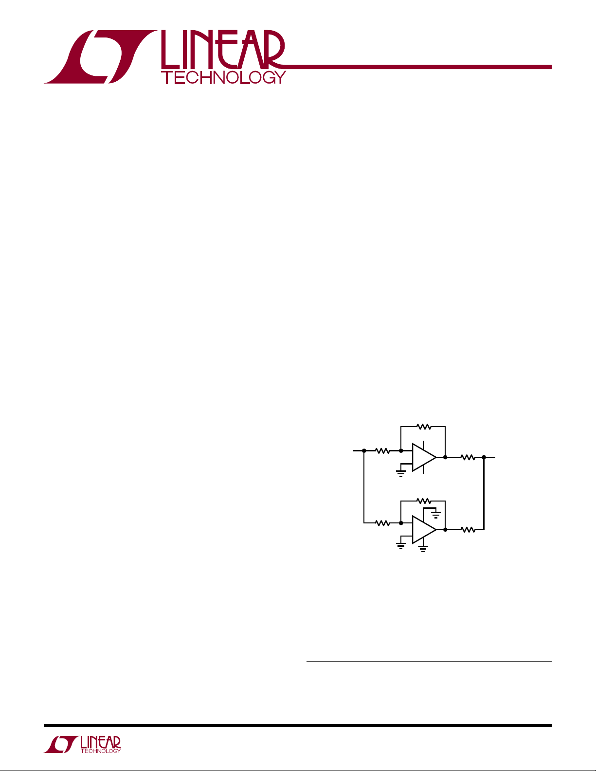
example. In Figure 1 an RH/LT1013 op amp is powered off
with its supply pins at circuit ground while other circuitry
is active and presents ±10V potentials through resistors
to the –IN pin and the OUTPUT pin.
10k
15V
INPUT
10V
10k
10k
–
+
–15V
10k
–
+
+
–
+
–
LT1013
LT1013
–10V
2k
2k
OUTPUT
AN141 F01
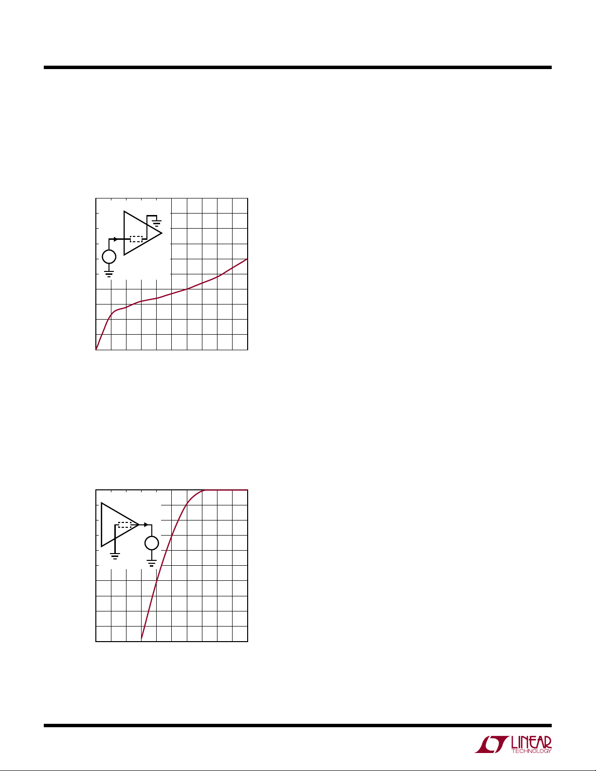
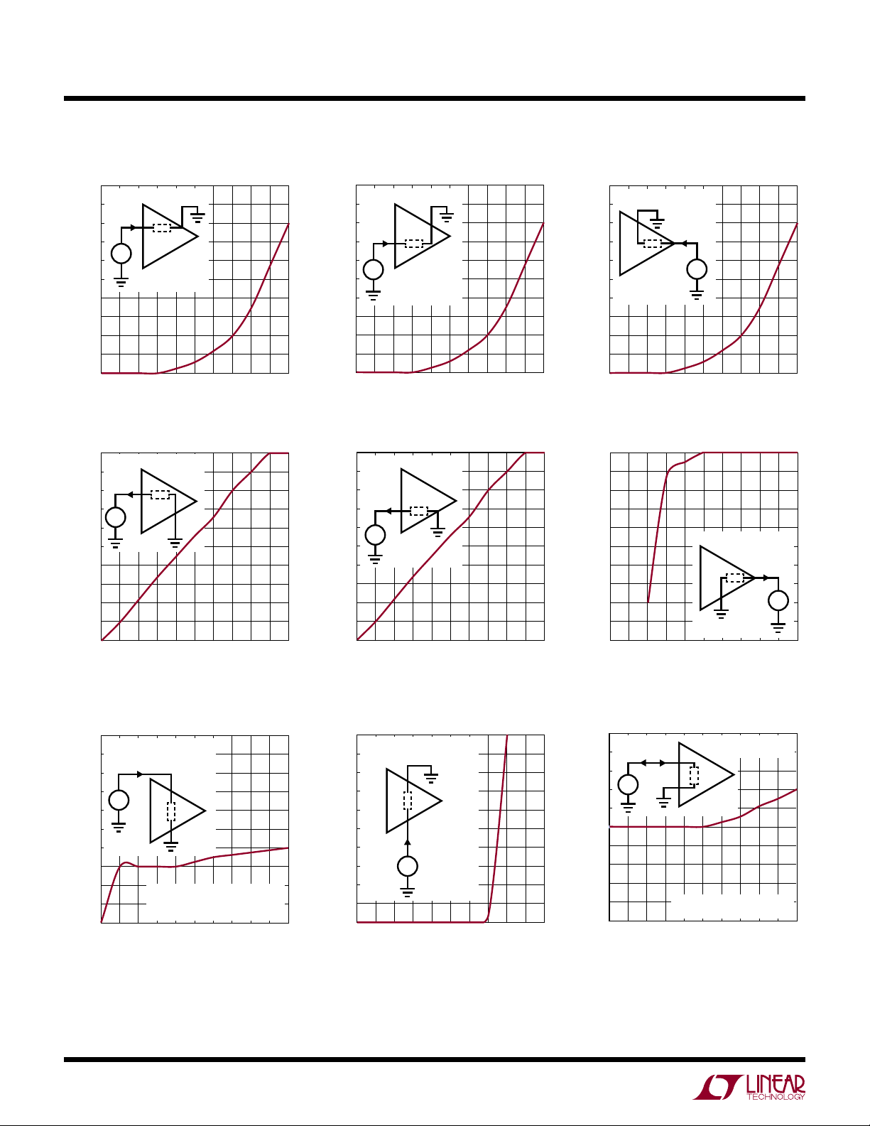
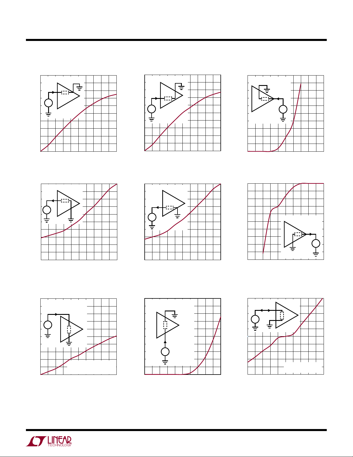
How to Interpret This Information?
For each amplifier a set of curve trace plots is provided.
These
plots indicate the expected current flow should the
inputs and output be connected to voltages outside the
supply rails.
Also shown is a plot of a normal supply connection voltage
sweep which indicates the amplifier’s start-up characteristic. A note added to this plot states at what point to expect
a supply overvoltage condition where the supply current
begins to increase rapidly.
Figure 1. Example of Unpowered Redundant Circuitry
The input condition will try to pull the –IN pin positive.
–
Pulling this input above the V
supply rail is normal circuit
operation for the RH/LT1013 so not a problem, but pull-
+
ing it above the V
L, LT, LTC, LTM, Linear Technology and the Linear logo are registered trademarks of Linear
Technology Corporation. All other trademarks are the property of their respective owners.
supply rail is abnormal and needs to
an141f
AN141-1
Page 2
Application Note 141
be checked. Refer to the plot for the RH/LT1013 showing
+
the –IN to V
characteristic, as shown in Figure 2. With
an input resistor of 10k the maximum current flow will be
1mA. At 1mA the –IN pin will pull up to near +1V. This plot
shows that this input pin could be pulled to 50V above
+
with 30mA of input current without damage. The input
V
biasing condition of this example is likely to be quite safe.
50
LT1013 –IN TO V
45
40
I
35
+
V
30
–
25
5mA/DIV
20
15
10
5
0
0
Figure 2. RH/LT1013 –IN Above V+ Plot
+
+
V
+
–
25 4515 35
5V/DIV
5020 405 10 30
AN141 F02
The output is being pulled negative through 4k of resistance.
–
Checking the OUT to V
plot for this amplifier, Figure 3,
shows that the output will clamp at a diode drop below
0
5
10
15
20
25
5mA/DIV
30
35
40
45
50
–2
LT1013 OUT TO V
+
–
V
–
I
_
–
V
+
–1 –0.2–1.4 –0.6
200mV/DIV
0–1.2 –0.4–1.8 –1.6 –0.8
AN141 F03
–
rail, approximately –0.7V with 2.5mA of current
the V
flow. This internal diode is fairly large and as shown in the
plot can safely conduct 10’s of mAs. This condition will
not likely cause any damage to the unpowered amplifier.
Another consequence of this condition however is loading
of the powered amplifier caused by the output clamping
of the unpowered amplifier. In this example the powered
amplifier must be able to sink the 2.5mA of current to
output the –10V level expected. If the powered amplifier
is from another RH/LT1013 package, it is able to sink this
much current so operation should be as expected. Other
lower power amplifiers may not have the output current
capability and the circuit output will be in error caused
by the loading interaction from the unpowered amplifier.
Use of these plots can provide a good starting point for
the evaluation of the risk of circuit damage and/or potential
erroneous operation of systems subjected to abnormal
supply connections. To help locate the plots for a particular
amplifier this index is provided:
INDEX
Amplifier Equivalent Tested Device Page
LT6016 LT6016 4
OP07 5
RH07
RH1013
RH1014
RH1028
RH1078
RH108
RH1056
RH118
RH1128
RH1498
RH1499
RH1814
RH27
RH37
RH6200
LT1013 6
LT1014 7
LT1028 8
LT1078 9
LM108 10
LT1056 11
LM118 12
LT1028 8
LT1498 13
LT1498 13
LT1814 14
LT1007 15
LT1007 15
LT6200 16
Figure 3. RH/LT1013 OUT Below V
AN141-2
–
Plot
an141f
Page 3

Application Note 141
Tips and Disclaimers
1. These measurements were taken on typical production
devices.
2. The majority of RH devices are electrically equivalent
to the commercial LT version of the same device. Most
of these measurements were taken on LT devices. The
effects of radiation dosing is not addressed in this study.
3. This information is to be considered as typical room
temperature performance. For characterization tem
perature behavior or radiation effects, the specific LT
or RH die is highly recommended to obtain optimal
data. No guarantee of device compliance to these
measurements is to be assumed. Absolute Maximum
Ratings apply. Check data sheet for more information.
4. The intent of these measurements is solely to provide
advice for what to expect under abnormal biasing condi
tions.
Most amplifiers contain built-in protection circuitry at
5.
input and output pins, primarily for ESD protection. This
circuitry is designed to redirect potentially destructive
current from sensitive transistor structures.
-
-
6. A current of 10mA or less into or out of any pin of
these amplifiers is generally considered safe and nondestructive short term or long term. Applied voltages
less than the maximum rated supply voltage of the
amplifier will be less likely to cause adverse transistor
voltage breakdown effects.
7. A curve tracer sweeps the applied voltage for some
measure of repetitive application. Long term effects
or degradation from long term continuous or repetitive
overvoltage conditions is not part of this study. If the
current is flowing primarily through a simple protection
diode it can generally be considered safe for the long
term.
8. These tests were performed with voltage applied only
to the indicated pins. Unless otherwise indicated the
power supply pins of the amplifiers are open circuited.
9. After the curve trace testing, these units were verified
to still have normal functionality in a typical application
circuit on a lab bench setup at room temperature. They
were not fully retested for all data sheet specifications
on an automated production test system.
an141f
AN141-3
Page 4
Application Note 141
AN141 G02
AN141 G08
Amplifier Type: LT6016 Similar Devices: LT6015, LT6016, LT6017 Tested Device: LT6016
200
180
160
140
120
100
20µA/DIV
80
60
40
20
0
0
0
0.5
1.0
1.5
2.0
2.5
0.5mA/DIV
3.0
3.5
4.0
4.5
5.0
–5
LT6016 +IN TO V
I
+
+
–
V
–
LT6016 +IN TO V
+
I
–
–
V
+
+
+
V
50 9030 70
10V/DIV
+IN to V
–
–
V
–2.5 –0.5–3.5 –1.5
0.5V/DIV
+IN to V
200
LT6016 –IN TO V
180
160
140
120
100
20µA/DIV
10040 8010 20 60
AN141 G01
I
+
V
–
80
60
40
20
0
0
+
0
LT6016 –IN TO V
0.5
AN141 G04
1.0
1.5
2.0
2.5
0.5mA/DIV
3.0
3.5
4.0
4.5
03 –1–4.5 –4 2
5.0
I
–
V
+
–5
–
+
–
+
–
+
+
V
50 9030 70
10V/DIV
–IN to V
–
–
V
–2.5 –0.5–3.5 –1.5
0.5mV/DIV
–IN to V
10040 8010 20 60
+
03 –1–4.5 –4 2
AN141 G05
–
200
180
160
140
120
100
20µA/DIV
80
60
40
20
0
0
0
2
4
6
8
10
2mA/DIV
12
14
16
18
20
–1
LT6016 OUT TO V
+
V
+
–
OUT
OUT to V
+
I
+
V
–
50 9030 70
10V/DIV
LT6016 OUT TO V
+
–
–0.5 –0.1–0.7 –0.3
100mV/DIV
OUT to V
10040 8010 20 60
AN141 G03
+
–
I
–
V
–
V
+
0–0.6 –0.2–0.9 –0.8 –0.4
–
AN141 G06
2000
LT6016 V+ TO V
1800
NORMAL POWER SUPPLY
1600
1400
1200
1000
200µA/DIV
800
600
400
200
I
+
+
V
–
–
SUPPLY VOLTAGE BREAKDOWN
BEGINS AT 72V. AT BREAKDOWN
I
0
0
SUPPLY
V+ to V– (Normal Supply) V– to V+ (Reverse Supply) +IN to –IN (Differential Input)
AN141-4
–
+
V
–
V
INCREASES TO 1200µA.
25 4515 35
5V/DIV
AN141 G07
5.0
LT6016 V– TO V
4.5
REVERSE POWER APPLIED
4.0
3.5
3.0
2.5
0.5mA/DIV
2.0
1.5
1.0
0.5
0
5020 405 10 30
0
+
+
V
+
–
–
V
I
+
V
–
50 9030 70
10V/DIV
10040 8010 20 60
1000
800
600
400
200
0
200µA/DIV
–200
–400
–600
–800
–1000
–50
LT6016 +IN TO –IN
I
+
–
V
+
–
DIFFERENTIAL INPUT
+
–
DIFFERENT CHARACTERISTIC
WITH POWER SUPPLIED
0 40–20 20
10V/DIV
AN141 G09
an141f
50–10 30–40 –30 10
Page 5
Application Note 141
AN141 G18
AN141 G17
Amplifier Type: RH07 Similar Devices: OP07 Tested Device: OP07
50
45
40
35
30
25
5mA/DIV
20
15
10
5
0
0
0
5
10
15
20
25
5mA/DIV
30
35
40
45
50
–20
OP-07 +IN TO V
I
+
+
–
V
–
OP-07 +IN TO V
+
I
–
–
V
+
+
+
V
10 186 14
2V/DIV
+IN to V
–
–
V
–10 –2–14 –6
2V/DIV
+IN to V
50
OP-07 –IN TO V
45
40
I
35
+
30
V
25
5mA/DIV
208 162 4 12
AN141 G10
–
20
15
10
5
0
0
+
0
OP-07 –IN TO V
5
10
15
–
20
V
25
5mA/DIV
0–12 –4–18 –16 –8
AN141 G13
+
30
35
40
45
50
–20
–
+
+
V
+
–
10 186 14
2V/DIV
–IN to V
–
+
208 162 4 12
AN141 G11
+
I
–
–
V
–10 –2–14 –6
2V/DIV
–IN to V
0–12 –4–18 –16 –8
AN141 G14
–
100
90
80
70
60
50
10mA/DIV
40
30
20
10
0
0
0
5
10
15
20
25
5mA/DIV
30
35
40
45
50
–2
OP-07 OUT TO V
+
V
+
–
OUT
+
I
+
V
–
1 1.80.6 1.4
200mV/DIV
OUT to V
OP-07 OUT TO V
+
–
–1 –0.2–1.4 –0.6
200mV/DIV
OUT to V
20.8 1.60.2 0.4 1.2
AN141 G12
+
–
I
–
V
–
V
+
0–1.2 –0.4–1.8 –1.6 –0.8
AN141 G15
–
20
OP-07 V+ TO V
18
NORMAL POWER SUPPLY
16
14
12
10
2mA/DIV
I
+
V
–
8
6
4
2
0
0
V+ to V– (Normal Supply) V– to V+ (Reverse Supply) +IN to –IN (Differential Input)
–
+
V
+
–
–
V
SUPPLY VOLTAGE BREAKDOWN
BEGINS AT 48V. AT BREAKDOWN
INCREASES TO 9mA.
I
SUPPLY
25 4515 35
5V/DIV
AN141 G16
50
OP-07 V– TO V
45
REVERSE POWER APPLIED
40
35
30
25
5mA/DIV
20
15
10
05
0
5020 405 10 30
0
+
+
V
+
–
–
V
I
+
V
–
0.5 0.90.3 0.7
100mV/DIV
10.4 0.80.1 0.2 0.6
10
8
6
4
2
0
2mA/DIV
–2
–4
–6
–8
–10
–5
I
+
+
–
V
+
–
–
OP-07 +IN TO –IN
DIFFERENTIAL INPUT
0 4–2 2
1V/DIV
5–1 3–4 –3 1
an141f
AN141-5
Page 6

Application Note 141
AN141 G22
AN141 G26
AN141 G21
AN141 G27
Amplifier Type: RH1013 Similar Devices: LT1013 Tested Device: LT1013
20
18
16
14
12
10
2mA/DIV
8
6
4
2
0
0
0
2
4
6
8
10
2mA/DIV
12
14
16
18
20
–10
LT1013 +IN TO V
I
+
+
–
V
–
LT1013 +IN TO V
+
I
–
–
V
+
+
+
V
25 4515 35
5V/DIV
+IN to V
–
–
V
–5 –1–7 –3
1V/DIV
+IN to V
50
LT1013 –IN TO V
45
AN141 G19
40
35
30
25
5mA/DIV
20
15
10
5020 405 10 30
I
+
V
–
5
0
0
+
0
LT1013 –IN TO V
2
4
6
–
8
V
10
2mA/DIV
0–6 –2–9 –8 –4
+
12
14
16
18
20
–10
–
+
+
V
+
–
25 4515 35
5V/DIV
–IN to V
–
+
5020 405 10 30
AN141 G20
+
I
–
–IN to V
–
V
–5 –1–7 –3
1V/DIV
–
0–6 –2–9 –8 –4
AN141 G23
50
45
40
35
30
25
LT1013 OUT TO V
5mA/DIV
20
15
10
5
0
0
0
5
10
15
20
25
5mA/DIV
30
35
40
45
50
–2
+
V
+
–
OUT
I
+
V
–
+
1 1.80.6 1.4
200mV/DIV
OUT to V
LT1013 OUT TO V
+
–
–1 –0.2–1.4 –0.6
200mV/DIV
OUT to V
+
–
V
–
20.8 1.60.2 0.4 1.2
–
I
–
V
+
0–1.2 –0.4–1.8 –1.6 –0.8
AN141 G24
1000
LT1013 V+ TO V
NORMAL POWER SUPPLY
900
800
SUPPLY VOLTAGE BREAKDOWN
BEGINS AT 60V. AT BREAKDOWN
700
600
500
100µA/DIV
400
300
200
100
0
INCREASES TO 640µA.
I
SUPPLY
0
V+ to V– (Normal Supply) V– to V+ (Reverse Supply) +IN to –IN (Differential Input)
AN141-6
–
5V/DIV
I
+
V
–
25 4515 35
50
LT1013 V– TO V
45
REVERSE POWER
APPLIED
40
35
+
30
25
–
+
V
+
–
–
V
5020 405 10 30
AN141 G25
5mA/DIV
20
15
10
5
0
0
+
+
V
–
V
I
+
V
–
1 1.80.6 1.4
200mV/DIV
20.8 1.60.2 0.4 1.2
10
8
6
4
2
0
2mA/DIV
–2
–4
–6
–8
–10
–5
I
+
+
–
V
+
–
–
LT1013 +IN TO –IN
DIFFERENTIAL INPUT
DIFFERENT CHARACTERISTIC
WITH POWER SUPPLIED
0 4–2 2
1V/DIV
5–1 3–4 –3 1
an141f
Page 7

Application Note 141
AN141 G28
AN141 G30
AN141 G36
Amplifier Type: RH1014 Similar Devices: LT1014 Tested Device: LT1014
20
18
16
14
12
10
2mA/DIV
8
6
4
2
0
0
0
2
4
6
8
10
2mA/DIV
12
14
16
18
20
–10
+IN to V
LT1014 +IN TO V
+
I
–
–
V
+
+IN to V
LT1014 +IN TO V
I
+
V
–
25 4515 35
5V/DIV
+
–
–
V
–5 –1–7 –3
1V/DIV
–
50
LT1014 –IN TO V
45
40
35
+
+
V
+
–
5020 405 10 30
0–6 –2–9 –8 –4
AN141 G31
30
25
5mA/DIV
20
15
10
10
2mA/DIV
12
14
16
18
20
+
V
–
5
0
0
0
LT1014 –IN TO V
2
4
6
–
8
V
+
–10
I
I
+
–
+
–
+
+
V
25 4515 35
5V/DIV
–IN to V
–
–
V
–5 –1–7 –3
1V/DIV
–IN to V
5020 405 10 30
AN141 G29
+
0–6 –2–9 –8 –4
AN141 G32
–
50
45
40
35
30
25
5mA/DIV
20
15
10
5
0
0
0
5
10
15
20
25
5mA/DIV
30
35
40
45
50
–2
+
V
+
–
OUT
LT1014 OUT TO V
+
–
–
V
LT1014 OUT TO V
I
+
V
–
+
1 1.80.6 1.4
200mV/DIV
OUT to V
I
–
V
+
–
–1 –0.2–1.4 –0.6
200mV/DIV
OUT to V
20.8 1.60.2 0.4 1.2
+
0–1.2 –0.4–1.8 –1.6 –0.8
AN141 G33
–
5.0
4.5
4.0
V
3.5
3.0
2.5
0.5mA/DIV
2.0
1.5
1.0
0.5
0
0
I
+
–
+
V
+
–
–
V
SUPPLY VOLTAGE BREAKDOWN
BEGINS AT 80V. AT BREAKDOWN
INCREASES TO 1.7mA.
I
SUPPLY
25 4515 35
5V/DIV
LT1014 V+ TO V
NORMAL POWER
SUPPLY
AN141 G34
–
5020 405 10 30
50
45
40
35
30
25
5mA/DIV
20
15
10
5
0
0
LT1014 V– TO V
REVERSE POWER
APPLIED
+
–
1 1.80.6 1.4
200mV/DIV
+
+
V
–
V
I
+
V
–
20.8 1.60.2 0.4 1.2
AN141 G35
10
8
6
4
2
0
2mA/DIV
–2
–4
–6
–8
–10
–5
I
+
+
–
V
+
–
–
DIFFERENT CHARACTERISTIC
WITH POWER SUPPLIED
1V/DIV
V+ to V– (Normal Supply) V– to V+ (Reverse Supply) +IN to –IN (Differential Input)
LT1014 +IN TO –IN
DIFFERENTIAL INPUT
0 4–2 2
an141f
AN141-7
5–1 3–4 –3 1
Page 8

Application Note 141
AN141 G39
AN141 G43
Amplifier Type: RH1028, RH1128 Similar Devices: LT1028, LT1128 Tested Device: LT1028
50
45
40
35
30
25
5mA/DIV
20
15
10
5
0
0
0
10
20
30
40
50
10mA/DIV
60
70
80
90
100
–2
LT1028 +IN TO V
I
+
+
–
V
–
+
+
V
1 1.80.6 1.4
200mV/DIV
+IN to V
V
–1 –0.2–1.4 –0.6
200mV/DIV
+IN to V
+
LT1028 +IN TO V
+
I
–
–
+
–
AN141 G37
–
–
V
AN141 G40
100
LT1028 –IN TO V
90
80
I
70
+
60
V
50
100
–
40
30
20
10
0
0
0
10
20
30
40
50
60
70
80
90
–2
10mA/DIV
20.8 1.60.2 0.4 1.2
10mA/DIV
0–1.2 –0.4–1.8 –1.6 –0.8
+
–
+
+
V
1 1.80.6 1.4
200mV/DIV
–IN to V
V
–1 –0.2–1.4 –0.6
200mV/DIV
–IN to V
+
LT1028 –IN TO V
+
I
–
–
+
–
AN141 G38
–
–
V
AN141 G41
20.8 1.60.2 0.4 1.2
0–1.2 –0.4–1.8 –1.6 –0.8
100
90
80
70
60
50
10mA/DIV
40
30
20
10
0
0
0
10
20
30
40
50
10mA/DIV
60
70
80
90
100
–10
LT1028 OUT TO V
+
V
+
–
OUT
+
–
–
V
LT1028 OUT TO V
+
I
+
V
–
1 1.80.6 1.4
200mV/DIV
OUT to V
I
–
V
+
–
–5 –1–7 –3
1V/DIV
OUT to V
20.8 1.60.2 0.4 1.2
+
0–6 –2–9 –8 –4
AN141 G42
–
10
I
9
+
8
7
6
5
1mA/DIV
4
3
2
1
0
0
+
V
–
–
V+ to V– (Normal Supply) V– to V+ (Reverse Supply) +IN to –IN (Differential Input)
AN141-8
LT1028 V+ TO V
+
V
V
SUPPLY VOLTAGE BREAKDOWN
BEGINS AT 52V. AT BREAKDOWN
I
SUPPLY
NORMAL POWER
SUPPLY
–
INCREASES TO 7mA.
10 186 14
2V/DIV
–
208 162 4 12
100
90
80
70
60
50
10mA/DIV
40
30
20
10
0
0
LT1028 V– TO V
REVERSE POWER
APPLIED
+
–
+
+
V
–
V
I
+
V
–
1 1.80.6 1.4
200mV/DIV
20.8 1.60.2 0.4 1.2
AN141 G44
10
8
6
4
2
0
2mA/DIV
–2
–4
–6
–8
–10
–1
I
+
+
–
V
+
–
–
LT1028 +IN TO –IN
DIFFERENTIAL INPUT
0 0.8–0.4 0.4
500mV/DIV
1–0.2 0.6–0.8–0.6 0.2
AN141 G45
an141f
Page 9

Application Note 141
AN141 G48
AN141 G46
AN141 G52
Amplifier Type: RH1078 Similar Devices: LT1078, LT1079 Tested Device: LT1078
10
THIS INPUT COULD
9
ALSO APPEAR
SIMILAR TO THE
8
–IN TO V
RESPONSE SHOWN.
7
INPUT
6
CHARACTERISTIC
DEPENDS ON V
5
TRIMMING RESULT.
1mA/DIV
4
3
2
1
0
0
0
LT1078 +IN TO V
1
2
–
3
V
4
+
5
1mA/DIV
6
7
8
9
10
–5
10
LT1078 –IN TO V
9
+
LT1078 +IN TO V
OS
I
+
+
+
V
+
–
V
–
1 1.80.6 1.4
200mV/DIV
–
–
V
–2.5 –0.5–3.5 –1.5
0.5V/DIV
+
–
+IN to V
+
I
–
+IN to V
20.8 1.60.2 0.4 1.2
0–3 –1–4.5 –4 –2
AN141 G49
8
7
6
5
1mA/DIV
4
3
2
1
0
0
0
1
2
3
4
5
1mA/DIV
6
7
8
9
10
–5
I
+
V
–
LT1078 –IN TO V
I
–
V
+
+
–
+
–
+
+
V
200mV/DIV
–IN to V
–
0.5V/DIV
–IN to V
V
THIS INPUT COULD
ALSO APPEAR
SIMILAR TO THE
+
RESPONSE
+IN TO V
SHOWN. INPUT
CHARACTERISTIC
DEPENDS ON V
TRIMMING
RESULT.
1 1.80.6 1.4
+
–
–2.5 –0.5–3.5 –1.5
–
OS
AN141 G47
AN141 G50
20.8 1.60.2 0.4 1.2
0–3 –1–4.5 –4 –2
50
45
40
35
30
25
5mA/DIV
20
15
10
5
0
0
0
5
10
15
20
25
5mA/DIV
30
35
40
45
50
–2
LT1078 OUT TO V
+
V
+
–
OUT
LT1078 OUT TO V
+
–
–
V
+
I
+
V
–
1 1.80.6 1.4
200mV/DIV
OUT to V
–
I
–
V
+
–1 –0.2–1.4 –0.6
200mV/DIV
OUT to V
20.8 1.60.2 0.4 1.2
+
0–1.2 –0.4–1.8 –1.6 –0.8
AN141 G51
–
500
450
400
350
300
250
50µA/DIV
200
150
100
50
0
0
I
+
V
–
V
+
–
V
SUPPLY VOLTAGE BREAKDOWN
BEGINS AT 58V. AT BREAKDOWN
I
SUPPLY
LT1078 V+ TO V
+
NORMAL POWER
SUPPLY
–
INCREASES TO 120µA.
10 186 14
2V/DIV
–
208 162 4 12
50
45
40
35
30
25
5mA/DIV
20
15
10
5
0
0
LT1078 V– TO V
REVERSE POWER
APPLIED
+
–
+
+
V
–
V
I
+
V
–
0.5 0.90.3 0.7
100mV/DIV
10.4 0.80.1 0.2 0.6
AN141 G53
10
8
6
4
2
0
2mA/DIV
–2
–4
–6
–8
–10
–5
I
+
+
–
V
+
–
–
DIFFERENT CHARACTERISTIC
WITH POWER SUPPLIED
1V/DIV
V+ to V– (Normal Supply) V– to V+ (Reverse Supply) +IN to –IN (Differential Input)
LT1078 +IN TO –IN
DIFFERENTIAL INPUT
0 4–2 2
AN141 G54
an141f
AN141-9
5–1 3–4 –3 1
Page 10

Application Note 141
AN141 G50a
Amplifier Type: RH108 Similar Devices: LM108 Tested Device: LM308
20
18
16
14
12
10
2mA/DIV
8
6
4
2
0
0
0
5
10
15
20
25
5mA/DIV
30
35
40
45
50
–2
V
2.5 4.51.5 3.5
500mV/DIV
+IN to V
V
–1 –0.2–1.4 –0.6
200mV/DIV
+IN to V
LM308A +IN TO V
+
V
I
+
+
–
–
+
LM308A +IN TO V
I
AN141 G46a
+
–
–
+
–
AN141 G49a
20
18
16
14
V
+
AN141 G47a
+
52 40.5 1 3
–
–
V
0–1.2 –0.4–1.8 –1.6 –0.8
+
52 40.5 1 3
–
–
V
0–1.2 –0.4–1.8 –1.6 –0.8
12
10
2mA/DIV
8
6
4
2
0
0
0
5
10
15
20
25
5mA/DIV
30
35
40
45
50
–2
LM308A –IN TO V
V
2.5 4.51.5 3.5
500mV/DIV
–IN to V
LM308A –IN TO V
V
–1 –0.2–1.4 –0.6
200mV/DIV
–IN to V
+
I
–
+
–
+
+
I
–
–
+
–
50
45
40
35
30
25
5mA/DIV
20
15
10
5
0
0
0
LM308A OUT TO V
5
+
10
15
–
20
25
5mA/DIV
30
35
40
45
50
–5
500mV/DIV
OUT to V
I
V
–
V
500mV/DIV
OUT to V
LM308A OUT TO V
+
V
+
–
2.5 4.51.5 3.5
+
–
–
+
–2.5 –0.5–3.5 –1.5
–
OUT
+
I
+
V
–
52 40.5 1 3
AN141 G48a
0–3 –1–4.5 –4 –2
AN141 G51a
500
450
400
350
300
250
50µA/DIV
200
150
100
I
+
+
V
–
–
SUPPLY VOLTAGE BREAKDOWN
50
0
0
BEGINS AT 65V. AT BREAKDOWN
I
SUPPLY
V+ to V– (Normal Supply) V– to V+ (Reverse Supply) +IN to –IN (Differential Input)
AN141-10
LM308A V+ TO V
+
NORMAL POWER
V
SUPPLY
–
V
INCREASES TO 270µA.
10 186 14
2V/DIV
–
AN141 G52a
50
LM308A V– TO V
45
REVERSE POWER
APPLIED
40
35
+
30
25
–
5mA/DIV
20
15
10
5
0
208 162 4 12
0
+
+
V
–
V
I
+
V
–
1 1.80.6 1.4
200mV/DIV
20.8 1.60.2 0.4 1.2
AN141 G53a
10
8
6
4
2
0
2mA/DIV
–2
–4
–6
–8
–10
–2.5
I
+
+
–
V
+
–
–
LM308A +IN TO –IN
DIFFERENTIAL INPUT
DIFFERENT CHARACTERISTIC
WITH POWER SUPPLIED
0 2–1 1
500mV/DIV
AN141 G54a
2.5–0.5 1.5–2 –1.5 0.5
an141f
Page 11

Application Note 141
AN141 G58
AN141 G59
AN141 G60
Amplifier Type: RH1056 Similar Devices: LT1055, LT1056, LT1057 Tested Device: LT1056
10
9
8
7
6
5
1mA/DIV
4
3
2
1
0
0
0
5
10
15
20
25
5mA/DIV
30
35
40
45
50
–5
LT1056 +IN TO V
I
+
+
–
V
–
LT1056 +IN TO V
+
I
–
–
V
+
+
+
V
50 9030 70
10V/DIV
+IN to V
–
–
V
–2.5 –0.5–3.5 –1.5
500mV/DIV
+IN to V
10
LT1056 –IN TO V
9
8
I
7
+
6
V
5
1mA/DIV
10040 8010 20 60
AN141 G55
–
4
3
2
1
0
0
+
0
10
20
30
40
50
10mA/DIV
60
70
80
90
100
0–3 –1–4.5 –4 –2
–2
–
+
–
+
+
V
50 9030 70
10V/DIV
–IN to V
–1 –0.2–1.4 –0.6
200mV/DIV
–IN to V
+
LT1056 –IN TO V
+
I
–
–
V
+
–
AN141 G56
–
–
V
10040 8010 20 60
0–1.2 –0.4–1.8 –1.6 –0.8
100
90
80
70
60
50
10mA/DIV
40
30
20
10
0
0
0
10
20
30
40
50
10mA/DIV
60
70
80
90
100
–2
LT1056 OUT TO V
+
V
+
–
OUT
OUT to V
+
I
+
V
–
1 1.80.6 1.4
200mV/DIV
LT1056 OUT TO V
+
–
–1 –0.2–1.4 –0.6
200mV/DIV
OUT to V
20.8 1.60.2 0.4 1.2
AN141 G57
+
–
I
–
V
–
V
+
0–1.2 –0.4–1.8 –1.6 –0.8
–
5.0
4.5
4.0
3.5
3.0
2.5
0.5mA/DIV
2.0
1.5
1.0
0.5
I
+
+
V
–
–
SUPPLY VOLTAGE BREAKDOWN
BEGINS AT 55V. AT BREAKDOWN
INCREASES TO 7mA.
I
SUPPLY
0
0
+
V
–
V
5V/DIV
LT1056 V+ TO V
NORMAL POWER
SUPPLY
25 4515 35
–
AN141 G61
50
45
40
35
30
25
5mA/DIV
20
15
10
5
0
5020 405 10 30
0
LT1056 V– TO V
REVERSE POWER
APPLIED
+
–
1 1.80.6 1.4
200mV/DIV
+
+
V
–
V
I
+
V
–
20.8 1.60.2 0.4 1.2
AN141 G62
2.5
2.0
1.5
+
1.0
–
0.5
0
0.5mA/DIV
–0.5
–1.0
–1.5
–2.0
–2.5
–50
I
+
–
V
+
–
LT1056 +IN TO –IN
DIFFERENTIAL INPUT
DIFFERENT CHARACTERISTIC
WITH POWER SUPPLIED
10V/DIV
V+ to V– (Normal Supply) V– to V+ (Reverse Supply) +IN to –IN (Differential Input)
AN141-11
0 40–20 20
50–10 30–40 –30 10
AN141 G63
an141f
Page 12

Application Note 141
AN141 G72
Amplifier Type: RH118 Similar Devices: LM118 Tested Device: LM118
100
90
80
70
60
50
10mA/DIV
40
30
20
10
0
0
0
5
10
15
20
25
5mA/DIV
30
35
40
45
50
–5
LM118 +IN TO V
I
+
+
–
V
–
LM118 +IN TO V
+
I
–
–
V
+
+
+
V
2.5 4.51.5 3.5
500mV/DIV
+IN to V
–
–
V
–2.5 –0.5–3.5 –1.5
500mV/DIV
+IN to V
100
LM118 –IN TO V
90
AN141 G64
80
70
60
50
10mA/DIV
40
30
20
10
52 40.5 1 3
I
+
V
–
0
0
+
0
LM118 –IN TO V
5
AN141 G67
10
15
20
25
5mA/DIV
30
35
40
45
0–3 –1–4.5 –4 –2
50
I
–
V
+
–5
–
+
–
+
–
+
+
V
2.5 4.51.5 3.5
500mV/DIV
–IN to V
–
–
V
–2.5 –0.5–3.5 –1.5
500mV/DIV
–IN to V
52 40.5 1 3
AN141 G65
+
0–3 –1–4.5 –4 –2
AN141 G68
–
100
90
80
70
60
50
10mA/DIV
40
30
20
10
0
0
0
5
10
15
20
25
5mA/DIV
30
35
40
45
50
–5
LM118 OUT TO V
+
V
+
–
OUT
OUT to V
LM118 OUT TO V
+
–
–
V
+
I
+
V
–
1 1.80.6 1.4
200mV/DIV
–
I
–
V
+
–2.5 –0.5–3.5 –1.5
500mV/DIV
OUT to V
20.8 1.60.2 0.4 1.2
AN141 G66
+
0–3 –1–4.5 –4 –2
AN141 G69
–
10
I
9
+
8
7
6
5
1mA/DIV
4
3
2
1
0
0
+
V
–
–
V+ to V– (Normal Supply) V– to V+ (Reverse Supply) +IN to –IN (Differential Input)
AN141-12
LM118 V+ TO V
+
NORMAL POWER
V
SUPPLY
–
V
SUPPLY VOLTAGE BREAKDOWN
BEGINS AT 45V. AT BREAKDOWN
INCREASES TO 4.2mA.
I
SUPPLY
10 186 14
2V/DIV
–
AN141 G70
50
LM118 V– TO V
45
REVERSE POWER
APPLIED
40
35
+
30
–
25
5mA/DIV
20
15
10
5
208 162 4 12
0
0
+
+
V
–
V
I
+
V
–
1 1.80.6 1.4
200mV/DIV
20.8 1.60.2 0.4 1.2
AN141 G71
2.5
2.0
1.5
+
1.0
–
0.5
0
0.5mA/DIV
–0.5
–1.0
–1.5
–2.0
–2.5
–5
I
+
–
V
+
–
LM118 +IN TO –IN
DIFFERENTIAL INPUT
DIFFERENT CHARACTERISTIC
WITH POWER SUPPLIED
0 4–2 2
1V/DIV
5–1 3–4 –3 1
an141f
Page 13

Application Note 141
AN141 G87
AN141 G89
AN141 G90
Amplifier Type: RH1498, RH1499 Similar Devices: LT1498, LT1499 Tested Device: LT1498
50
45
40
35
30
25
5mA/DIV
20
15
10
5
0
0
0
5
10
15
20
25
5mA/DIV
30
35
40
45
50
–2
LT1498 +IN TO V
I
+
+
–
V
–
+
+
V
1 1.80.6 1.4
200mV/DIV
+IN to V
V
–1 –0.2–1.4 –0.6
500mV/DIV
+IN to V
+
LT1498 +IN TO V
+
I
–
–
+
–
AN141 G82
–
–
V
AN141 G85
50
LT1498 –IN TO V
45
40
I
35
+
30
V
25
5mA/DIV
20.8 1.60.2 0.4 1.2
5mA/DIV
0–1.2 –0.4–1.8 –1.6 –0.8
–
20
15
10
5
0
0
0
5
10
15
20
25
30
35
40
45
50
–2
+
–
+
+
V
1 1.80.6 1.4
200mV/DIV
–IN to V
V
–1 –0.2–1.4 –0.6
200mV/DIV
–IN to V
+
LT1498 –IN TO V
+
I
–
–
+
–
AN141 G83
–
–
V
AN141 G86
20.8 1.60.2 0.4 1.2
0–1.2 –0.4–1.8 –1.6 –0.8
50
45
40
35
30
25
5mA/DIV
20
15
10
5
0
0
0
5
10
15
20
25
5mA/DIV
30
35
40
45
50
–2
+
–
–
V
LT1498 OUT TO V
1 1.80.6 1.4
200mV/DIV
OUT to V
I
–
V
+
–
–1 –0.2–1.4 –0.6
200mV/DIV
OUT to V
LT1498 OUT TO V
+
V
+
–
OUT
+
–
+
I
+
V
–
20.8 1.60.2 0.4 1.2
AN141 G84
0–1.2 –0.4–1.8 –1.6 –0.8
10
9
8
7
6
5
1mA/DIV
4
3
2
1
0
0
I
+
+
V
–
–
SUPPLY VOLTAGE BREAKDOWN
BEGINS AT 43V. AT BREAKDOWN
I
SUPPLY
LT1498 V+ TO V
+
NORMAL POWER
V
SUPPLY
–
V
INCREASES TO 3.6mA.
10 186 14
2V/DIV
–
208 162 4 12
AN141 G88
50
45
40
35
30
25
5mA/DIV
20
15
10
5
0
0
LT1498 V– TO V
REVERSE POWER
APPLIED
+
–
+
+
V
–
V
I
+
V
–
0.5 0.90.3 0.7
100mV/DIV
10.4 0.80.1 0.2 0.6
25
20
15
10
5
0
5mA/DIV
–5
–10
–15
–20
–25
–2.5
I
+
+
–
V
+
–
–
DIFFERENT CHARACTERISTIC
WITH POWER SUPPLIED
500mV/DIV
V+ to V– (Normal Supply) V– to V+ (Reverse Supply) +IN to –IN (Differential Input)
AN141-13
LT1498 +IN TO –IN
DIFFERENTIAL INPUT
0 2–1 1
2.5–0.5 1.5–2 –1.5 0.5
an141f
Page 14

Application Note 141
AN141 G100
AN141 G101
AN141 G102
Amplifier Type: RH1814 Similar Devices: LT1814 Tested Device: LT1814
50
45
40
35
30
25
5mA/DIV
20
15
10
5
0
0
0
5
10
15
20
25
5mA/DIV
30
35
40
45
50
–2
LT1814 +IN TO V
I
+
+
–
V
–
LT1814 +IN TO V
+
I
–
–
V
+
+
+
V
1 1.80.6 1.4
200mV/DIV
+IN to V
–
–
V
–1 –0.2–1.4 –0.6
200mV/DIV
+IN to V
50
LT1814 –IN TO V
45
40
I
35
+
30
V
25
5mA/DIV
20.8 1.60.2 0.4 1.2
–
20
15
10
5
0
0
+
0
LT1814 –IN TO V
5
10
I
15
–
20
V
25
5mA/DIV
0–1.2 –0.4–1.8 –1.6 –0.8
AN141 G103
+
30
35
40
45
50
–2
–
+
–
+
–
+
+
V
1 1.80.6 1.4
200mV/DIV
–IN to V
–
–
V
–1 –0.2–1.4 –0.6
200mV/DIV
–IN to V
20.8 1.60.2 0.4 1.2
+
0–1.2 –0.4–1.8 –1.6 –0.8
AN141 G104
–
50
45
40
35
30
25
5mA/DIV
20
15
10
5
0
0
0
5
10
15
20
25
5mA/DIV
30
35
40
45
50
–2
+
–
–
V
LT1814 OUT TO V
+
–
1 1.80.6 1.4
200mV/DIV
OUT to V
I
–
V
+
–
–1 –0.2–1.4 –0.6
200mV/DIV
OUT to V
LT1814 OUT TO V
+
V
I
OUT
+
–
AN141 G105
+
+
V
–
20.8 1.60.2 0.4 1.2
0–1.2 –0.4–1.8 –1.6 –0.8
20
I
18
+
16
14
12
10
2mA/DIV
8
6
4
2
0
0
+
V
–
–
SUPPLY VOLTAGE BREAKDOWN
BEGINS AT 20V. AT BREAKDOWN
I
SUPPLY
V+ to V– (Normal Supply) V– to V+ (Reverse Supply) +IN to –IN (Differential Input)
AN141-14
LT1814 V+ TO V
+
V
V
NORMAL POWER
SUPPLY
–
INCREASES TO 12mA.
5 93 7
1V/DIV
–
AN141 G106
50
LT1814 V– TO V
45
REVERSE POWER
APPLIED
40
35
+
30
25
–
5mA/DIV
20
15
10
5
0
104 81 2 6
0
+
+
V
–
V
I
+
V
–
0.5 0.90.3 0.7
100mV/DIV
1.00.4 0.80.1 0.2 0.6
AN141 G107
25
20
15
10
5
0
5mA/DIV
–5
–10
–15
–20
–25
–2.5
I
+
+
–
V
+
–
–
LT1814 +IN TO –IN
DIFFERENTIAL INPUT
DIFFERENT CHARACTERISTICS
WITH POWER SUPPLIED
0 2–1 1
0.5V/DIV
AN141 G108
an141f
2.5–0.5 1.5–2 –1.5 0.5
Page 15

Application Note 141
AN141 G110
AN141 G116
Amplifier Type: RH27, RH37 Similar Devices: OP27, OP37, LT1007, LT1037 Tested Device: LT1007
100
90
80
70
60
50
10mA/DIV
40
30
20
10
0
0
0
10
20
30
40
50
10mA/DIV
60
70
80
90
100
–2
LT1007 +IN TO V
I
+
+
–
V
–
+
+
V
2.5 4.51.5 3.5
500mV/DIV
+IN to V
–1 –0.2–1.4 –0.6
200mV/DIV
+IN to V
+
LT1007 +IN TO V
+
I
–
–
V
+
–
AN141 G109
–
–
V
AN141 G112
100
LT1007 –IN TO V
90
80
I
70
+
60
V
50
–
10mA/DIV
40
30
20
10
52 40.5 1 3
0–1.2 –0.4–1.8 –1.6 –0.8
0
0
0
10
20
30
40
50
10mA/DIV
60
70
80
90
100
–2
+
–
+
+
V
500mV/DIV
–IN to V
200mV/DIV
–IN to V
2.5 4.51.5 3.5
+
LT1007 –IN TO V
+
I
–
–
V
+
–1 –0.2–1.4 –0.6
–
–
–
V
AN141 G113
52 40.5 1 3
0–1.2 –0.4–1.8 –1.6 –0.8
100
90
80
70
60
50
10mA/DIV
40
30
20
10
0
0
0
5
10
15
20
25
5mA/DIV
30
35
40
45
50
–2
LT1007 OUT TO V
+
V
+
–
OUT
OUT to V
+
I
+
V
–
1 1.80.6 1.4
200mV/DIV
LT1007 OUT TO V
+
–
–1 –0.2–1.4 –0.6
200mV/DIV
OUT to V
20.8 1.60.2 0.4 1.2
AN141 G111
+
–
I
–
V
–
V
+
0–1.2 –0.4–1.8 –1.6 –0.8
–
AN141 G114
5.0
LT1007 V+ TO V
NORMAL POWER
4.5
SUPPLY
4.0
SUPPLY VOLTAGE BREAKDOWN
3.5
BEGINS AT 56V. AT BREAKDOWN
I
SUPPLY
3.0
2.5
0.5mA/DIV
2.0
1.5
1.0
0.5
0
0
–
INCREASES TO 3.6mA.
V
5 93 7
1V/DIV
100
LT1007 V– TO V
90
REVERSE POWER
APPLIED
80
70
+
60
50
I
+
–
+
V
+
–
–
V
104 81 2 6
AN141 G115
10mA/DIV
40
30
20
10
0
0
–
+
+
V
–
V
I
+
V
–
1 1.80.6 1.4
200mV/DIV
20.8 1.60.2 0.4 1.2
25
20
15
10
5
0
5mA/DIV
–5
–10
–15
–20
–25
–2.5
I
+
+
–
V
+
–
–
500mV/DIV
V+ to V– (Normal Supply) V– to V+ (Reverse Supply) +IN to –IN (Differential Input)
Information furnished by Linear Technology Corporation is believed to be accurate and reliable.
However, no responsibility is assumed for its use. Linear Technology Corporation makes no representation that the interconnection of its circuits as described herein will not infringe on existing patent rights.
AN141-15
LT1007 +IN TO –IN
DIFFERENTIAL INPUT
0 2–1 1
AN141 G117
2.5–0.5 1.5–2 –1.5 0.5
an141f
Page 16

Application Note 141
AN141 G119
AN141 G121
AN141 G122
AN141 G123
Amplifier Type: RH6200 Similar Devices: LT6200 Tested Device: LT6200
50
45
40
35
30
25
5mA/DIV
20
15
10
5
0
0
0
5
10
15
20
25
5mA/DIV
30
35
40
45
50
–2
LT6200 +IN TO V
+
V
I
+
+
–
V
–
LT6200 +IN TO V
+
I
–
–
V
+
+
1 1.80.6 1.4
200mV/DIV
+IN to V
–
–
V
–1 –0.2–1.4 –0.6
200mV/DIV
+IN to V
50
LT6200 –IN TO V
45
40
I
35
+
30
V
25
–
5mA/DIV
20
15
10
5
20.8 1.60.2 0.4 1.2
AN141 G118
0
0
+
0
LT6200 –IN TO V
5
10
I
15
–
20
V
25
5mA/DIV
0–1.2 –0.4–1.8 –1.6 –0.8
+
30
35
40
45
50
–2
–
+
–
+
–
+
+
V
200mV/DIV
–IN to V
–
V
200mV/DIV
–IN to V
1 1.80.6 1.4
+
–
–1 –0.2–1.4 –0.6
–
20.8 1.60.2 0.4 1.2
0–1.2 –0.4–1.8 –1.6 –0.8
50
45
40
35
30
25
5mA/DIV
20
15
10
5
0
0
0
5
10
15
20
25
5mA/DIV
30
35
40
45
50
–2
LT6200 OUT TO V
+
V
+
–
OUT
OUT to V
+
I
+
V
–
1 1.80.6 1.4
200mV/DIV
LT6200 OUT TO V
+
–
–1 –0.2–1.4 –0.6
200mV/DIV
OUT to V
20.8 1.60.2 0.4 1.2
AN141 G120
+
–
I
–
V
–
V
+
0–1.2 –0.4–1.8 –1.6 –0.8
–
50
LT6200 V+ TO V
NORMAL POWER
45
SUPPLY
40
SUPPLY VOLTAGE BREAKDOWN
35
BEGINS AT 20V. AT BREAKDOWN
I
SUPPLY
30
25
5mA/DIV
20
15
10
5
0
0
–
INCREASES TO 15mA.
V+ to V– (Normal Supply) V– to V+ (Reverse Supply) +IN to –IN (Differential Input)
AN141-16
50
LT6200 V– TO V
45
REVERSE POWER
APPLIED
V
5 93 7
1V/DIV
40
35
30
I
+
–
+
V
+
–
–
V
104 81 2 6
AN141 G124
25
5mA/DIV
20
15
10
5
0
0
+
V
+
–
–
V
I
+
V
–
Linear Technology Corporation
1630 McCarthy Blvd., Milpitas, CA 95035-7417
(408) 432-1900 ● FAX: (408) 434-0507
●
www.linear.com
+
0.5 0.90.3 0.7
100mV/DIV
AN141 G125
25
20
15
10
5
0
5mA/DIV
–5
–10
–15
–20
–25
10.4 0.80.1 0.2 0.6
–1
I
+
+
–
V
+
–
LINEAR TECHNOLOGY CORPORATION 2013
–
LT6200 +IN TO –IN
DIFFERENTIAL INPUT
0 0.8–0.4 0.4
200mV/DIV
LT 1013 • PRINTED IN USA
AN141 G126
1–0.2 0.6–0.8–0.6 0.2
an141f
 Loading...