

Page 1
Power Supply Layout and EMI
Christian Kueck
Application Note 139
October 2012
Introduction
PC-board layout determines the success or failure of every
power supply project. It sets functional, electromagnetic
interference (EMI), and thermal behavior. Switching power
supply layout is not black magic, but is often overlooked
until it is too late in the design process. Fortunately physics
is on your side. Functional and EMI requirements must
be met, and in a world of trade-offs in power supply unit
layout, what is good for functional stability is good for
EMI. Good layout from first prototyping on does not add
to cost, but actually saves significant resources in EMI
filters, mechanical shielding, EMI test time and PC board
runs. This application note focuses primarily on nonisolated
topologies, but will examine some isolated topologies as
well. You will learn to make the optimum choices regarding
PC-board layout for solid power supply designs.
I remember about a dozen years ago as a customer was
using a switch mode power supply in a car radio for the
first time many of his colleagues said that it could not
be done. However, after a few things were ironed out in
layout and input filtering, everything worked fine. Later a
®
customer successfully used an LT
1940 1MHz dual stepdown switching regulator, which operated in the middle
of his AM band in a car radio receiver. No additional metal
shielding was required for the power supply unit (PSU);
it was only an issue of placement and layout. In order to
get there, we need to go through some physics.
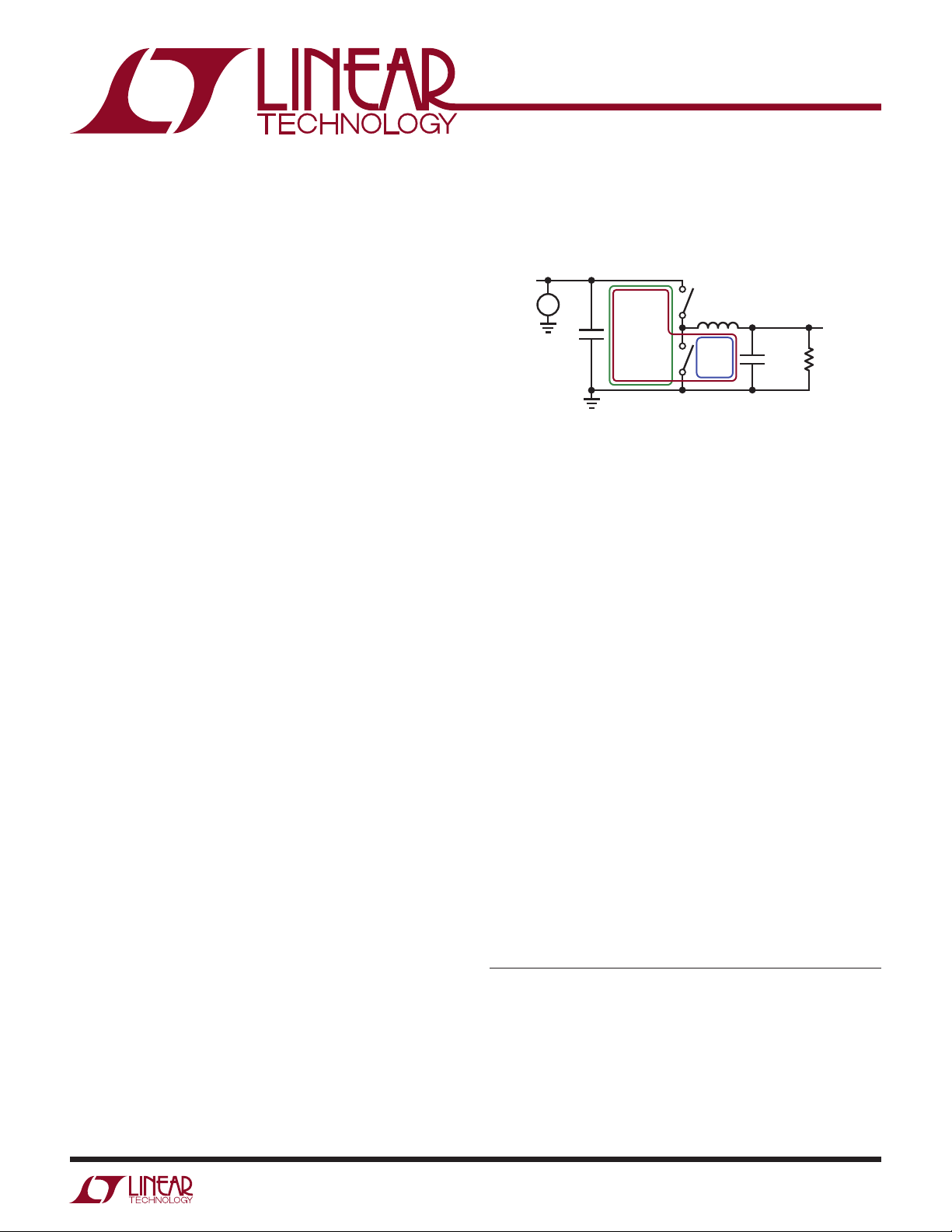
With nonisolated topologies, one of the most basic topologies is the buck regulator. EMI starts off from high di/dt
loops. The supply wire as well as the load wire should not
have high AC current content. So we can focus our analysis from the input capacitor, C
relevant AC currents to the output capacitor, C
, which should source all
IN
, where
OUT
any AC currents end.
V
IN
+
–
C
IN
HOT LOOP
S1
S2
Figure 1
V
OUT
C
OUT
AN139 F01
During the on cycle with S1 closed and S2 open, the AC
current follows the red loop (Figure 1). During the off
cycle, with S1 open and S2 closed, the AC current follows
the blue loop. Both currents have a trapeze shape. People
often have difficulty grasping that the loop producing the
highest EMI is not the red nor the blue loop. Only in the
green loop flows a fully switched AC current, switched from
zero to I
and back to zero. We refer to the green loop
PEAK
as a hot loop, since it has the highest AC and EMI energy.
In order to reduce EMI and improve functionality, you
need to reduce the radiating effect of the green loop as
much as possible. If we could reduce the PC-board area
of the green loop to zero and buy an ideal input capacitor
with zero impedance, the problem would be solved. But
we are limited to the real world. The task of engineering
is to find the optimal compromise.
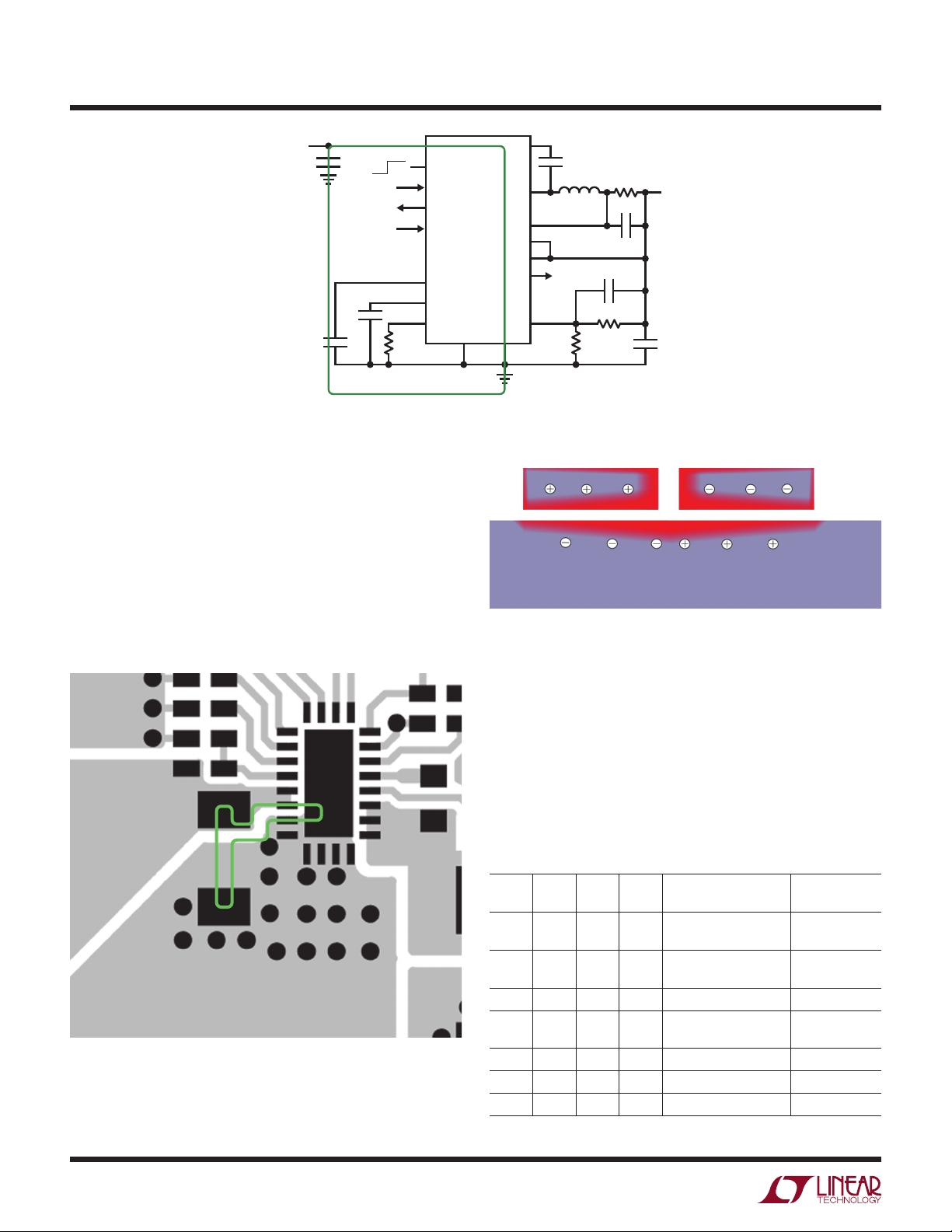
Let’s take a look at the layout of an LT8611 buck converter
(Figure 3). The LT8611 has both switches internal, so we
only have to be concerned with the connection of the
input capacitor.
As you can see from the schematic in Figure 2, the hot
loop is not easy to spot for layout purposes.
L, LT, LTC, LTM, Linear Technology, the Linear logo and LTspice are registered trademarks of
Linear Technology Corporation. All other trademarks are the property of their respective owners.
an139fa
AN139-1
Page 2
Application Note 139
V
IN
5.5V TO 42V
f
SW
4.7μF
0.1μF
1μF
= 700kHz
The green line is the hot loop in the top layer. AC current
flows through the input capacitor and the switches in the
part. Figure 3 shows the DC1750A LT8611 demo board.
The current density in the cross cut of the hot loop will
look like this (Figure 4).
60.4k
IN
EN/UVON OFF
SYNC
IMON
ICTRL
INTV
TR/SS
RT
LT8611
CC
Figure 2
BSTV
SW
ISP
ISN
BIAS
PG
FB
GNDPGND
0.1μF
4.7μH
243k
10pF
1M
0.02Ω
1μF
AN139 F02
V
5V
2.5A
47μF
OUT
How much does a copper short-circuit loop or plane under
the hot loop improve the functional and EMI behavior of
your circuit?
AN139 F03
Figure 3
Figure 4
The result of an experiment with a 10 cm × 10cm rectangular
loop with 27MHz is shown in Table 1. The table gives an
indication how much improvement a solid copper plane
under the hot loop topside traces gives. The first line is
no plane single layer.
The inductance of a single-layer loop of 187nH gets down
to 13nH in the case of only 0.13mm insulation between
the plane and loop traces.
Table 1
d
(mm)f (MHz) C (pF) L (nH)
18.4 400 187 Single-Layer Open
Loop
21.2 400 141 Inner Copper ShortCircuit Loop
1.5 38.9 400 42 Solid Plate 3.23
1.5 34.7 400 53 Rectangular Loop No
Overlap
0.5 52.1 400 23 Thin Rectangular 1.77
0.27 55 400 21 1.61
0.12 69 400 13 Paper
FACTOR OVER
0.12mm
14.4
10.85
4.08
AN139-2
an139fa
Page 3
Application Note 139
A solid plane on the next layer in a multilayer board
(four layers or more) will have over 3× less inductance
than a normal 1.5mm 2-layer board with a solid bottom
plane, and over 14× less over a single-layer board. A solid
plane with minimum distance to the hot loop is one of the
most effective ways to reduce EMI.
Where Does the Current Flow in the Plane?
The green top layer hot loop magnetic AC field produces
eddy currents in the plane (Figure 5). Those eddy currents
produce a mirror AC magnetic field, which is opposite the
hot loop field (red trace). Both magnetic fields will cancel
out. This works better the closer the mirror current is to
the hot loop. Current is a round trip in the top layer. The
most likely current path in the shield is the same round
trip direct under the top layer. Both currents are almost the
same. Since the plane current needs to be as high as the
top trace current, it will produce as much voltage across
the plane as is necessary to sustain the current. To the
outside it will show up as GND bounce.
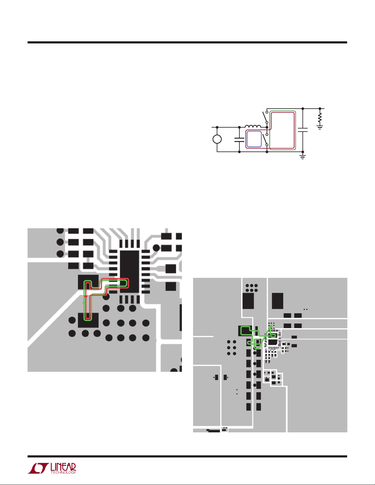
The boost circuit can be viewed in continuous mode as a
buck circuit operating backwards.
The hot loop is identified as the difference between the
blue loop if S2 is closed and the red loop (Figure 6) with
S2 open and S1 closed.
V
OUT
S1
V
IN
+
C
IN
–
S2
HOT LOOP
Figure 6
C
OUT
AN139 F06
The hot loop of the LT3956 LED driver boost controller
is shown in green (Figure 7). The second layer is a solid
GND plane. The main EMI emitter is the magnetic antenna the hot loop creates. The area of the hot loop and
its inductance are tightly related. If you are comfortable
thinking in inductance, try to decrease it as much as you
can. If you are more comfortable in antenna design, reduce
the effective area of the magnetic antenna. For near field
purposes, inductance and magnetic antenna effectiveness
are essentially the same. See Appendices A and B for
further background.
AN139 F05
Figure 5
From EMI perspective small hot loops are best. A power
supply IC with integrated sync switches, optimized pinout
and careful internal switch control will outperform on
EMI a non-sync power supply IC with external Schottky
diode. And both will outperform a controller solution with
external MOSFETs.
+LED
+OUT
PGND
Figure 7
PV
IN
PGND
AN139 F07
an139fa
AN139-3
Page 4

Application Note 139
The single inductor 4-switch buck-boost (Figure 8) consists
of a buck circuit followed by a boost circuit. The layout will
often be complicated by a common GND current shunt
®
which belongs to both hot loops. The LTC
3780 DC1046A
demo board (Figure 9) shows an elegant solution splitting
the sense resistor in two parallel ones.
AN139 F08
V
OUT
V
IN
+
–
HOT LOOP
HOT LOOP
Figure 8. 4-Switch Buck-Boost
A bit different drawing of a SEPIC circuit (Figure 10) shows
its hot loop. Instead of an active MOSFET for the top switch,
a diode is often used. The LT3757 DC1341A (Figure 11)
shows a good SEPIC layout. The green hot loop area is
minimized and has a solid GND plane on the next layer.
V
OUT
V
IN
+
–
Figure 10. SEPIC
HOT LOOP
AN139 F10
AN139-4
AN139 F09
Figure 9
an139fa
Page 5
Application Note 139
AN139 F11
Figure 11
The inverting topology (Figure 12) is very similar to SEPIC,
only the load has moved through the top switch and top
–V
OUT
inductor. Layout is very similar, and demo boards can
typically be modified from SEPIC to inverting provided
V
IN
+
–
HOT LOOP
AN139 F12
the IC can also regulate on negative feedback voltage like
LT3581, LT3757 etc..
Flyback (Figure 13) uses separate windings on a transformer and there is only magnetic coupling between the
primary and secondary windings. The current in the primary
Figure 12. Inverting
1
2
10mH
+–~
~
winding goes to zero at a relative high di/dt; only the energy
3
HOT LOOP
HOT LOOP
HIGH HF IMPEDANCE
Figure 13. Isolated Offline Flyback
AN139 F13
4
an139fa
AN139-5
Page 6
Application Note 139
stored in the leakage inductance and capacitance between
windings and on the switch node slows that down. The
primary and other transformer windings can be seen as
fully switched current. We get two main hot loops as in the
buck-boost case (Figure 8). To reduce EMI, in addition to
close V
decoupling for differential mode EMI, common
IN
mode chokes are used for the likely dominant common
mode EMI in this topology.
Other AC Loops
The hot loop with the main switching energy is the major
source of RF energy. However for the operation of the IC
and circuit, other AC carrying loops are required. All circuits
need a supply for the main switch driver. In the case of the
buck, it is often decoupled with the same V
capacitor as
IN
the hot loop. Other ICs use a separate voltage for the drive
circuit, often referred to as INTV
Make the INTV
capacitor PGND and GND loop as small
CC
(Figure 14).
CC
as possible and shield it with a solid plane in the next
layer. EMI energy is on the order of 20dB lower than in
the main hot loop. Any excessive inductance in the INTV
loop will deteriorate IC performance. The INTV
capacitor
CC
CC
decouples beside switch drive internal sensitive and wide
band circuitry like current sense comparators, reference
and error amplifiers which are very often internal supplied
from INTV
CC
too.
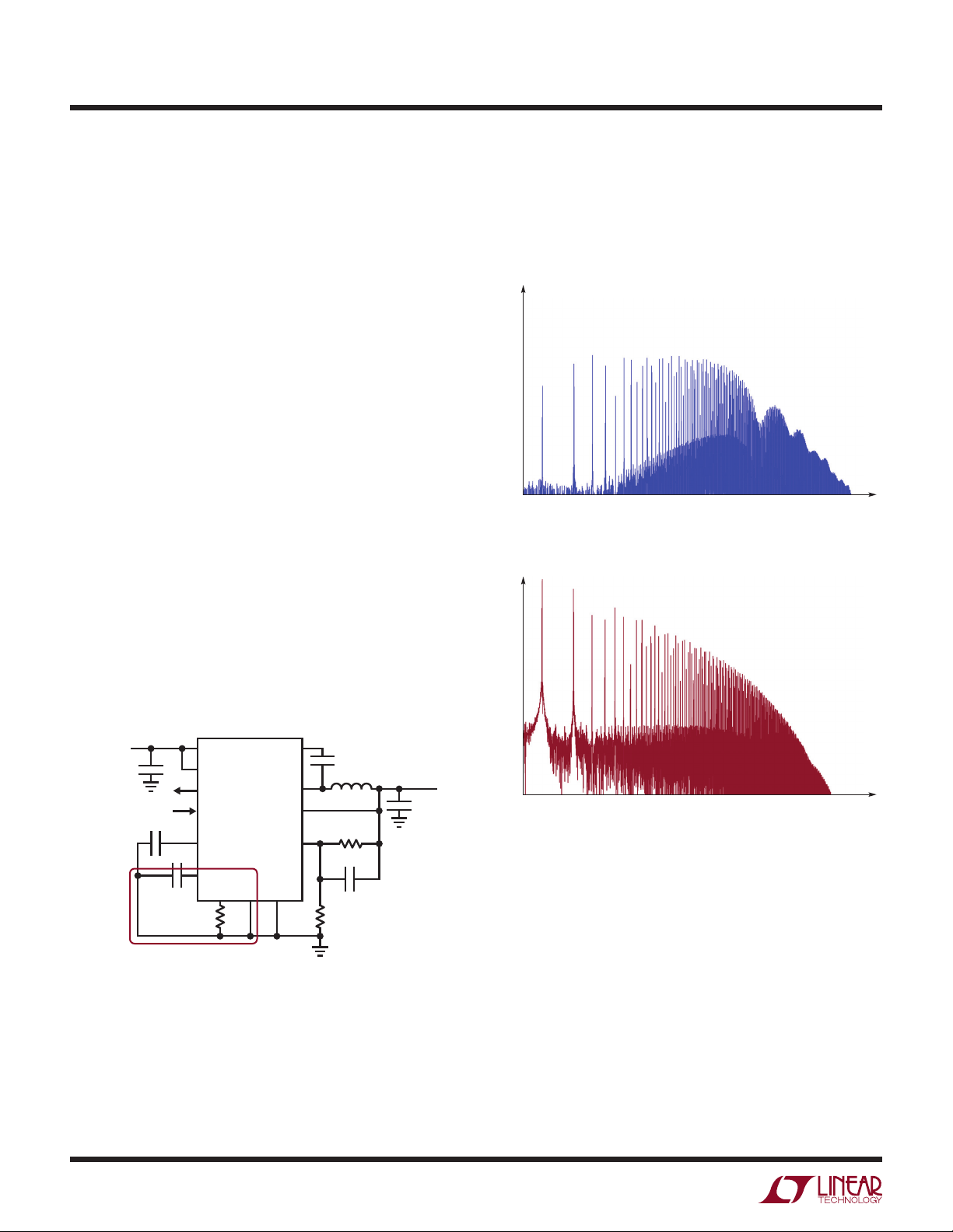
Figure 15 is an FFT of the current in the INTVCC decoupling
capacitor (C2 in Figure 17).
Figure 16 is an FFT of the current in the input capacitor
(C6 in Figure 17). The RF energy is over 20dB higher than
in the INTV
–10dB
–30dB
–50dB
–70dB
–90dB
–10dB
–30dB
–50dB
loop.
CC
I(C2)
1MHz 1GHz
100MHz10MHz
AN139 F15
Figure 15
I(C6)
V
5.5V TO 42V
4.7μF
IN
10nF
1μF
60.4k
IN
EN/UV
PG
SYNC
TR/SS
INTV
RT
CC
LT8610
PGND
GND
BSTV
SW
BIAS
0.1μF
4.7μH
FB
1M
10pF
243k
47μF
V
OUT
5V
2.5A
–70dB
–90dB
1MHz 1GHz
10MHz
100MHz
AN139 F16
Figure 16
The LT8610 LTspice
loss of R
= 1Ω is used to decouple the zero impedance
PAR
®
circuit (Figure 17) L2 with a high
LTspice voltage source, V1, from the input capacitor, C6.
Note: LTspice switch mode regulator models are developed
f
= 700kHz
SW
Figure 14
AN39 F14
to simulate the functionality of the IC. Use great caution
to extrapolate RF behavior because the models do not
account for the internal or the external lump devices or
board layout. However, it is nonetheless a great tool to
get an approximation of very difficult to measure effects.
an139fa
AN139-6
Page 7

L2
1μH
= 10mΩ
R
SER
= 1Ω
R
PAR
IN
V1
+
–
12V
C6
4.7μF
R
SER
L
SER
= 4mΩ
= 2nH
C1
0.001μF
R1
52.3k
EN/UV
MODE
PG
TR/SS
RT
GND
V
IN
LT8610
INTV
PGND
CC
BIAS
BST
SW
FB
Figure 17
External Switch Drive Signals
After the main hot loop and the INTV
decoupling loop,
CC
the next EMI trouble sources are often external switch
drive signals. Even modern MOSFETs have single-to-dual
digit nanofarad effective input capacitance. Their drivers
often have drive currents in the single amp range, with
rise and fall times approaching single digit nanoseconds.
R
L
SER
SER
–20dB
–40dB
–60dB
C2
1μF
= 4mΩ
= 1nH
C3
0.1μF
Application Note 139
L1
4.7μH
R2
1M
R3
432k
C5
10pF
C4
47μF
IG(Q2)
OUT
R
LOAD
1.32Ω
AN139 F17
Figure 18 is the FFT of the gate current into Q2 of Figure 19.
The green loop (Figure 19) shows the current path for
the bottom gate current. It is supplied from the C1. Make
sure that the loop is small. The Q2-source GND to C1 GND
connection is most easily accomplished with a solid GND
area in the next layer under the component layer.
C1
CC_INT
SENSE
SENSE
10μF
D1
1N5819
HG
C2
0.22μF
LG
+
–
FB
.TRAN 2.25m START-UP
Figure 19
V1 24V
V2 5V
C6 0.01μF
R4 82.5k
V3 1V
C5 0.01μF
C4 5.6nF
R
SER
+
–
+
EN/UVLO CBOOT
–
V
RT SW
+
CTRL1
–
CTRL2
SS
VC
= 39.2k
REF
V
IN
V
LT3741
GND
–80dB
–100dB
Q1
Si7884DP
L1 2.2μH
Q2
Si7884DP
1MHz
R1
2.5mΩ
Figure 18
R2
88.7k
R3
12.1k
AN139 F19
10MHz 100MHz
C3
300μF
AN139 F18
an139fa
AN139-7
Page 8

Application Note 139
The red and green loop (Figure 20) shows the top gate
drive current loops. They are supplied from the boost
capacitor, C2, and the return is the SW connection to the
controller IC. Keep the red loop small and place the traces
parallel with only a small gap. If C2 is placed close to the
controller IC, the green loop will also become small.
The green loop (Figure 21) shows the recharge of the boost
capacitor. If you have already made the above loops small
and have placed D1 relatively close, this loop is also small.
C1
CC_INT
SENSE
SENSE
10μF
D1
1N5819
HG
C2
0.22μF
LG
+
–
FB
.TRAN 2.25m START-UP
Figure 20
V1 24V
V2 5V
C6 0.01μF
R4 82.5k
V3 1V
C5 0.01μF
C4 5.6nF
R
SER
+
–
+
–
+
–
= 39.2k
V
V
IN
EN/UVLO CBOOT
V
REF
RT SW
LT3741
CTRL1
CTRL2
SS
VC
GND
Passive antennas, including magnetic antennas or loops,
operate reciprocally, and their transmit and receive characteristics are the same. The sense amplifier in Figure 22
+
looks with high bandwidth at SENSE
and SENSE– on the
small shunt voltage over R1 to terminate the top switch
on cycle.
Even sub-millivolt noise will result in duty cycle jitter.
Coupling to any of the former transmitting loops should
be minimal. First, this loop area needs to be small as well,
Q1
Si7884DP
L1 2.2μH
Q2
Si7884DP
R1
2.5mΩ
C3
300μF
R2
88.7k
R3
12.1k
AN139 F20
AN139-8
V1 24V
V2 5V
C6 0.01μF
R4 82.5k
V3 1V
C5 0.01μF
C4 5.6nF
= 39.2k
R
SER
+
–
V
+
EN/UVLO CBOOT
–
V
REF
RT SW
+
CTRL1
–
CTRL2
SS
VC
IN
LT3741
GND
V
CC_INT
SENSE
SENSE
HG
LG
+
–
FB
C1
10μF
D1
1N5819
C2
0.22μF
.TRAN 2.25m START-UP
Figure 21
Q1
Si7884DP
L1 2.2μH
Q2
Si7884DP
R1
2.5mΩ
C3
300μF
R2
88.7k
R3
12.1k
AN139 F21
an139fa
Page 9

V1 24V
V2 5V
C6 0.01μF
R4 82.5k
V3 1V
C5 0.01μF
C4 5.6nF
= 39.2k
R
SER
+
–
V
+
EN/UVLO CBOOT
–
V
REF
RT SW
+
CTRL1
–
CTRL2
SS
VC
IN
LT3741
GND
V
CC_INT
SENSE
SENSE
HG
LG
+
–
FB
C1
10μF
D1
1N5819
C2
0.22μF
.TRAN 2.25m START-UP
Figure 22
Q1
Si7884DP
L1 2.2μH
Q2
Si7884DP
Application Note 139
R1
2.5mΩ
C3
300μF
R2
88.7k
R3
12.1k
AN139 F22
so make the gap between the SENSE+ and SENSE– line
minimal. Then place the loop traces on the other side of
a shielding plane from the high current loops mentioned
+
above. If enough layers are available, the SENSE
–
SENSE
line can be on top of each other if there are not
and
significant magnetic AC fields parallel to the PC board
+
layers. If SENSE
and SENSE– filtering is used, place the
filter close to the controller IC, since R1 is always low
impedance and the sense inputs are higher impedance.
C1
CC_INT
SENSE
SENSE
10μF
D1
1N5819
HG
C2
0.22μF
LG
+
–
FB
V1 24V
V2 5V
C6 0.01μF
R4 82.5k
V3 1V
C5 0.01μF
C4 5.6nF
R
SER
+
–
+
–
+
–
= 39.2k
V
V
IN
EN/UVLO CBOOT
V
REF
RT SW
LT3741
CTRL1
CTRL2
SS
VC
GND
The main hot loop in Figure 23 consists of the external
MOSFETs Q1 and Q2 and the closest low impedance decoupling capacitor C7. This is the loop with the highest RF
energy in a controller solution. For a detailed discussion
of controller layout, see LTC Application Note136 [8].
C7
10μF
Q1
Si7884DP
L1 2.2μH
Q2
Si7884DP
.TRAN 2.25m START-UP
R1
2.5mΩ
C3
300μF
R2
88.7k
R3
12.1k
AN139 F23
Figure 23
an139fa
AN139-9
Page 10

Application Note 139
How Shielding Works
DC magnetic fields go through air, FR4 epoxy dielectric
and copper almost undisturbed.
AC magnetic fields are impacted only by the induced currents in a conductor—usually copper or tin, etc. So, absent
from ferromagnetic material, we can focus on currents as
the only source to alter or attenuate AC magnetic fields in
a typical PC board environment.
AN139 F24
Figure 24
We know from experiments that complete conductive
enclosures have a very high attenuation—easily over
100dB—over a very broad frequency range above the AM
band. Cookie boxes are a popular example widely used in
the R&D community to shield sensitive circuitry, to enable high frequency (HF) measurements. For HF circuits
you can buy them in rectangular form which fits easier
for PC boards and HF connectors like BNC, N, SMA, etc.
For practical purposes HF magnetic fields do not escape
closed conductive boxes as long as the wall is thicker than
skin depth (see Appendix C).
If we blow up the conductive enclosure like a balloon
large enough that it is a flat wall between us and the AC
current, the eddy currents in the shield material need to
create an AC magnetic field, which is the opposite of the
original AC current behind the wall (Figure 24). The eddy
currents in the shield will only be enough to cancel any
magnetic AC field to the outside of the box or, in our case,
in the direction shown at the lower portion of Figure 25.
How Effective is a Shield?
If the board copper plane were non-conductive, it would
be transparent to any magnetic field like a sheet of paper.
The current in the copper is the only source of influence
on the magnetic field. The energy available for eddy currents is induced in the shield. Such currents will cancel
any magnetic field inside the copper shield and outside in
the direction away from the inducing current, within the
limits of skin and proximity effect (Figure 26).
AN139 F26
Figure 26
The cancellation layer is the layer that cancels the magnetic field from the inducing currents (i.e., from the hot
loop) and induced currents in the shield. So it is sort of
midway between the AC currents in opposite directions.
The position of the cancellation layer can be estimated by
rule of thumb and may help you visualize how the remaining AC fields look.
The closer the cancellation layer is to the induced current
layer, the better the cancellation. Inductance is the integral
of the magnetic field—the same magnetic field that forms
the near field RF antenna. All of these effects are reduced
when the cancellation layer is placed closer to the inducing current loop.
AN139-10
Figure 25
AN139 F25
an139fa
Page 11

What Works Even Better?
If the current returns through the plane, the situation is
somewhat different (Figure 27). Now the current in the plane
is not only passive induced, but is the active return flow.
AN139 F27
Application Note 139
Figure 27
It is forced to be same as the current in the top trace.
The benefit is that the cancellation is now closer to the
inducing trace, in this case halfway between the top layer
current and the returning current in the plane. Because the
cancellation layer is now half the distance to the inducing
current, it is safe to say that the magnetic field is now
lower by at least a factor of two compared to the above
situation with passive shielding only.
If you can, let the return current flow in the closest layer.
Make its dielectric (isolation) as thin as practical. It is
better to have the return current flow in the closest trace
to the inducing current with minimum dielectric distance.
That’s what solid GND planes do by default.
Standard multilayer boards often have much thinner outer
layer dielectrics to help reduce EMI.
Line Conducted EMI Measurements
Figure 28 is an LT8611 with some input filtering with a ferrite bead and 4.7μF ceramics line conducted from 30MHz
to 400MHz. The display line of –67dBm corresponds to
40dBuV.
Figure 29 shows an LT8610 power supply 13V in, 5V out
at 1A out, line conducted up to 900MHz. In Figure 29
an additional wideband amplifier (LNA) in the HF signal
chain with 35dB gain is used. So the –100dBm spectrum
analyzer display line corresponds to –135dBm, which is
the thermal noise floor of a 50Ω system with 10kHz bandwidth at room temperature. The main HF energy needed
to be filtered out of the LT8610/LT8611 is below 400MHz.
+10dBuV corresponds to 3.16μV
RMS
.
AN139 F28
Figure 28
AN139 F29
Figure 29
EMI Optimization
First check the layer stack. Use a PC board of four layers
or more if possible. The second layer from top is typically
only about 200μm distance, and a shield will cancel the
hot loop much better than any shield over 1mm away in
a dual layer board.
In the hot loop shield, the same current as in the top trace
hot loop runs as eddy current. Keep the layer 2 shield
solid. Place vias away from the hot loop for connections
to GND planes you want to keep quiet. The hot loop shield
cancellation currents create HF voltage across the loop,
and you do not want to couple it with vias in areas you
need quiet. This current decays with distance, but often
remains a problem.
an139fa
AN139-11
Page 12

Application Note 139
The challenge for filtering the input and, if required, the
output is mainly in finding an area that is quiet enough.
An effective way is to make a complete GND ring around
the the power supply unit (PSU) connected with vias.
Filter capacitor GND return should be at the location where
the V
current crosses the ring. There should be still
IN
filtering inductance in the direction of the hot loop. That
can be a ferrite bead or an inductor.
Beware of magnetic coupling between filter inductors and
the main inductor. The transformer action can jeopardize
your attenuation. Place filter inductors at a distance from
the main inductor.
Use short ceramic capacitors, i.e., 0402, or reverse geometry capacitors because the block capacitors need low
APPENDIX A
Electromagnetic Field Impedance
Far field impedance is about 377Ω = 120π or 29,9792458
• 4 • πΩ for the vacuum velocity of light. Any electromagnetic wave far enough from its source (rule of thumb
>wavelength/2 • π) has a 377Ω relationship between its
magnetic and electric field. Closer to the source, it can be a
perfect matched antenna, which transforms its input power
source to the right 377Ω electromagnetic field. Or there
is significant mismatch and the antenna starts mainly as
a magnetic field source or an electric field source.
The magnetic field source has a lower impedance of
377Ω. The electric field source has a higher than 377Ω
impedance. The graph Figure 30 shows that, regardless
if it starts as an electric or a magnetic field source, the
electromagnetic field balances itself to its far field impedance at a distance of:
λ
2•π
Nonisolated switch mode power supply units have primarily magnetic field sources since the impedances of the
EMI-relevant loops with high di/dt are much lower than
377Ω unless you have very low current high voltage power
supplies. So minimizing the AC magnetic fields on any
nonisolated power supply unit will be the key to success.
equivalent series inductance (ESL) which mainly dictates
their impedance. Shorter and thicker ones have lower ESL.
See Appendix C for discussion.
Characteristic impedance of the strip lines you create
with your V
traces is in the low single digit Ohm area.
IN
The ESL of your block capacitors should be as low as
possible. Use reverse geometry capacitors or a stack of
0402 closest to the filter point and larger cases close by.
Any trace length significantly increases the few hundred
pH inductance your small block capacitors have. Ensure
that the routing path of the V
and the return trace go
IN
through the filter capacitor pads. This avoids additional
trace inductance.
Any isolated power supply unit will have AC loops with lower
than 377Ω, where the same magnetic field minimization
as on nonisolated PSUs will be required. However, due to
the very nature of isolation, we need higher impedances
between the isolation barrier. On the isolation barrier,
which is mostly done with a transformer, we try to get MΩ
of isolation. On the isolation barrier, the electric AC field
dominates and requires a different strategy. Here we try
to get as low capacitive field coupling as possible. So we
try to get as much distance as possible and to minimize
the size of any conductive material—i.e., copper.
10000
| (Ω)
W
|Z
5000
3000
2000
1000
500
300
200
100
50
30
20
10
0.01 0.02
ELECTRIC
FIELD SOURCE
MAGNETIC
FIELD SOURCE
NEAR FIELD FAR FIELD
0.05 0.1 0.2 0.5
1
2π
r
Q
Figure 30 [1]
1 2 5 10
AN138 F30
an139fa
AN139-12
Page 13

Application Note 139
APPENDIX B
Dipole Antenna Effect of the Hot Loop
When analyzing what the hot loop does, magnetic dipole
antennas give a good clue.
The AC current flows around an area and creates the
magnetic field part of a normal dipole antenna (Figure 31).
Magnetic antennas with loop diameters <<λ have very low
radiation resistance. Range μΩ to mΩ.
RR= 320π
4
⎢
⎥
2
λ
⎣
⎦
2
NF
⎡
⎤
RR = Radiation resistance in Ohm
F = Area of magnetic loop
N = Number of turns (= 1 in most layouts)
λ = Wavelength
with λ =
c
and N = 1 for all practical layout loops
f
4f4F2
320π
RR=
4
c
c = Speed of light ≈300000km/s
f = Frequency
[2]
The radiation resistance is low (mΩ) for typical dimensions of a PC-board power supply unit. Increasing the
radiation resistance improves the matching and increases
emitted radiation proportional to the radiation resistance.
The parameter we can influence the most with layout is
the area of the magnetic loop.
The emitted radiation is proportional to the square of this
area.
DIPOLE
Figure 31
F
AN139 F31
an139fa
AN139-13
Page 14

Application Note 139
APPENDIX C
Skin Effect
To understand the effect of shielding, we need to dig a bit
into the electromagnetic properties of the materials used.
Electric current, whether or not it is tied to a conductor,
will always flow on the path of least impedance. For higher
frequencies this will be the path of least inductance. This
means the current will also flow on the path of its lowest
losses. Electric conduction material minimizes any internal
magnetic AC fields by creating eddy currents that oppose
AC fields internal to the conducting material. Viewed from
the outside, this looks like skin effect, because the current
density is forced to the outside of the conductor.
For the first model example, assume that the current, I,
flows uniformly through a cylinder. This is a typical case
for DC current.
If the current is DC, then it will look like that in Figure 32.
Since I is constant, the resulting H is constant and I
is
W
zero. In the case that I has an AC content, which means
there is di/dt, then the resulting magnetic field H changes.
The changing magnetic field H creates induction voltage
and since we are inside a conductor, the induction voltage
creates an induced current I
, often referred to as eddy
W
current. Eddy currents will create losses. If we assume that
nature minimizes these losses, the only way to minimize
this is to change the original uniform current distribution
and let all current flow only at the surface of the cylinder.
AN139-14
AN139 F32
Figure 32 [3]
an139fa
Page 15

Application Note 139
Now the magnetic field H is only at the surface of the
cylinder. This way the eddy currents I
are moved to the
W
outside and the return path is cut off, omitting most of
the eddy currents and its losses.
We can think of forces (Figure 33) that move the current
density to the outside of a conductor
This is called skin effect. The wall thickness of a pipe, which
would give the same resistance at DC as a full cylinder wire
at AC, is called skin depth (Figure 34). Since the forces
moving the current density to the outside are a result of
the induction law, the skin depth goes down with rising
frequency. Skin depth goes down with rising conductivity
and goes down with increasing magnetic permeability.
For another example, assume we have a pipe wall conducting all the current on its surface, as shown in the
large diameter in Figure 35. Total inductance of a given
length of this wire (1 meter or 1 foot, whatever is most
suitable) is the complete volume integral of its magnetic
field up to infinity or whatever physical size you assume
for the universe.
Now we shrink the pipe diameter to the smaller inner one
shown in Figure 35. The magnetic field is still the same as
the old larger pipe to infinity. However, we now have an
additional magnetic field volume between the new small
pipe and the prior larger pipe diameter. So the total integral
of the magnetic field is now larger. This shows that the
Figure 33 [3]
Figure 34 [3]
AN139 F33
AN139 F34
AN139 F35
Figure 35
an139fa
AN139-15
Page 16

Application Note 139
inductance is larger for a thinner conductor of a given
length. Or we can assume that the inductance increases
as more of the current moves from the outer wall to the
center of the wire. If we apply a voltage over both ends of
the wire, the resulting current distribution is determined
by the impedance. Since the inductance in the center is
higher, most current density moves to the surface. The
most extreme case of skin effect we have in conductors
with zero resistance is shown in superconductors. There
quantum effects prevent all current from being bound
to an outer layer of zero thickness. The thickness where
most current is concentrated on superconductors is called
London depth.
A graph of skin depth over frequency for some materials
is shown in Figure 36.
100μm
10μm
We see that copper on typical PC-board material is affected
by skin effect starting in the 5MHz to 50MHz range. And
we can see that even highly doped silicon at the thickness
typically used on ICs is only affected in the terahertz region.
Copper (Cu) and gold (Au) are close together. Material with
high magnetic permeability (Fe-Ni) has low skin depth even
at audio frequencies. For this reason it is used to shield
audio transformers.
AC current through a good conductor will push current
density to the outside. The current will flow where the impedance, dominated by inductance, is lowest. With regard
to the impact of skin effect on layout and components,
we can derive simple guidelines. Better is short and thick
or wide. Reverse geometry capacitors have lower ESL
because they are shorter and thicker.
HIGHLY DOPED
SILICON 10**20
COPPER CLAD 35μm 2oz
25μm BOND WIRE
17μm 1oz
8.5μm 0.5oz
1μm
100nm
10k
TIN
Au
Cu
Fe-Ni
u-METAL
1M 100M100k 10M 1G 10G
FREQUENCY (Hz)
Figure 36
SUPERCONDUCTOR
(TYP 1.2 10nm TO 500nm)
AN139 F36
AN139-16
an139fa
Page 17

Application Note 139
APPENDIX D
Proximity Effect
If we have opposite direction current, the same forces
will attract the currents to each other (Figure 37). This is
called proximity effect.
If we have a PC board trace on a single layer board, the high
frequency current density will look like that in Figure 38.
If we add a solid plane in a second layer eddy currents will
be generated in the plane, creating in total a mirror image
of the current in the top trace, as shown in Figure 39.
On multilayer boards, a plane will shield the AC currents
(Figure 40).
Figure 37 [4]
AN139 F37
an139fa
AN139-17
Page 18

Application Note 139
AN139 F38
Figure 38
AN139 F39
Figure 39
Figure 40
AN139 F40
an139fa
AN139-18
Page 19

Application Note 139
APPENDIX E
EMI Measurements
Most power supplies are relatively small compared to the
wavelength of the relevant EMI frequencies they produce
and are measured against. If prudently designed, in current power supply technology you will find most energy
below 500MHz. EMI standards must be general and apply
to equipment of variable size. Those can be in the order of
the wavelength of interest. So they call for line conducted
measurements up to 30MHz and radiated measurements
above 30MHz. However reliable radiated measurements
require large anechoic chambers. Their hourly prices are
high and availability is scarce. Free field is too noisy, requires a large and difficult setup and is weather dependent.
For power supply optimization work, a reasonable approach
is to make line-conducted precompliance measurements
up to the end of the spectrum required for radiated measurements. Since the power supply dimensions are still
small against the wavelength of interest, we can assume
that most energy will find its way through the V
wires, where we can measure them line conducted.
V
OUT
and
IN
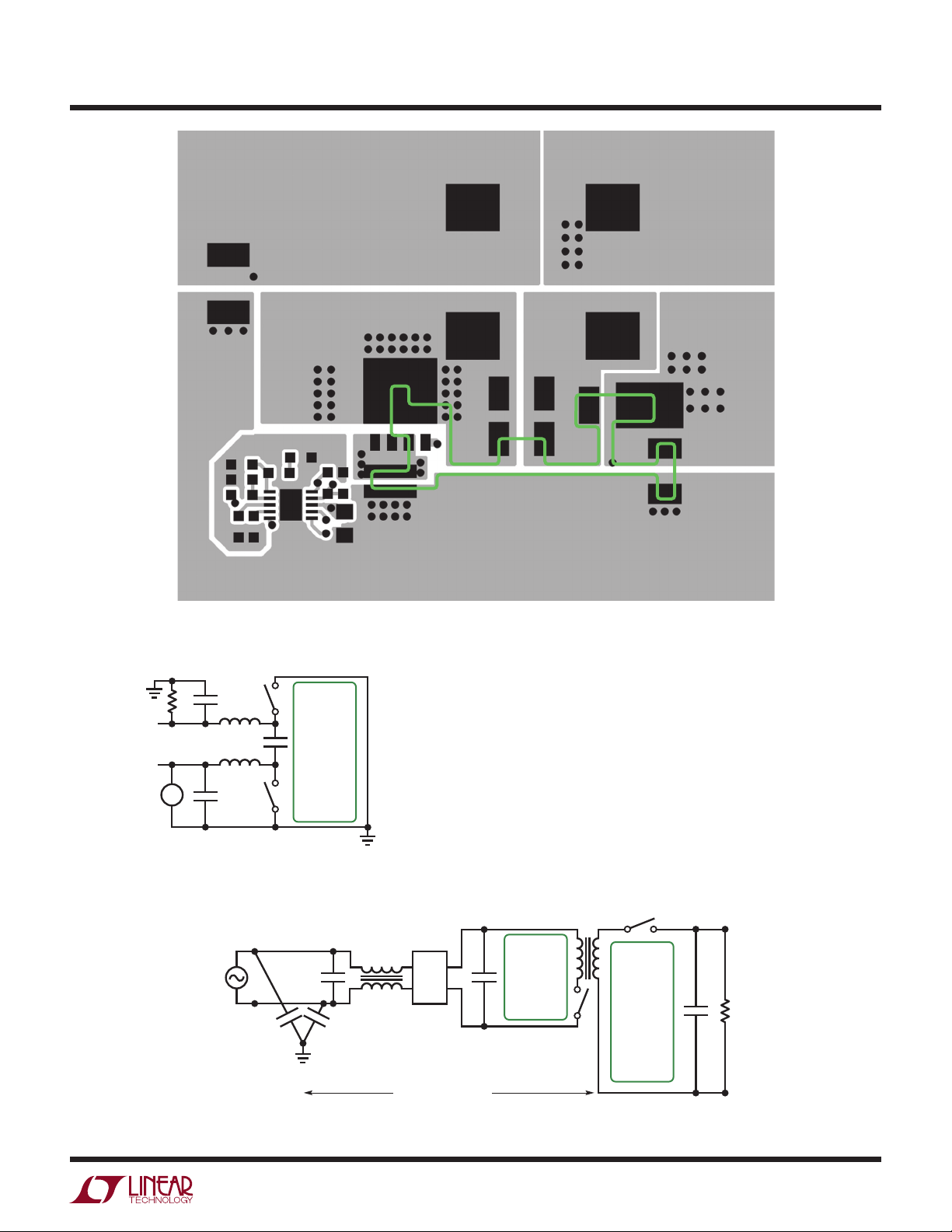
The setup is quite simple. We need a LISN (line impedance stabilizer network) or AN (artificial network), an input
supply, a load and a measurement receiver.
The purpose of the LISN (AN) is to isolate the voltage
source V1 from the power supply (or DUT device under
test) V
IN
(V
DUT
, V
DUT
).
+
This is an example of a non-symmetric LISN often used
in automotive (Figure 41). Such a simple circuit can be
made with L1 as air coil, or an inductor with losses can
be used. Some standards specify different core types in
series and a special winding scheme. However, the main
purpose is to create a wideband high impedance against
50Ω for L1.
LISN
L1
5μH
V1
+
–
12V
.TRAN 1
C2
100μF
R1
1k
C1
100nF
V
OUT_HF
R2
50Ω
V
DUT
V
DUT
AN139 F41
+
–
Other than the wire length inside for C1, R1 and the
V
and L1 impedance, nothing limits the usable
OUT_HF
upper frequency range. So buy one or build your own.
Resonances of L1 can be damped with a resistor over a
part of L1 windings.
Any dedicated EMI receiver can be used, but a spectrum
analyzer will usually do for precompliance work. Make
sure that you use the AC-coupled input, since it provides
a second barrier against blowing up your expensive mixer
inside the analyzer.
From the EMI lab experts, you can expect a lengthy discussion about the required detection method from the
used EMI standard, including peak, quasi peak, average
with relative accurate time constants required for them.
You can shortcut this discussion when your power supply operates fixed frequency in the load area of interest.
At fixed frequency, only harmonics with a distance of the
switching frequency can be created, a frequency comb.
If the switching frequency is above the required resolution bandwidth (mostly 9kHz up to 30MHz and 120kHz
above 30MHz), peak, quasi peak and average methods
will yield the same results, so you can use whatever your
receiver provides. Some standards allow for the 9kHz to
use a 10kHz bandwidth and for 120kHz 100kHz. The error
for a fixed frequency switching PSU, which operates well
above 100kHz, is not relevant for our precompliance task.
If your system includes a processor it can produce currents with large fluctuations with frequency contents well
within the above resolution bandwidth.
Then you need to refrain to the filter method your standard
requires.
If you see components that are a fraction of the switching
frequency or cannot be divided by integers to the switching
frequency, check the switch node with an oscilloscope.
In the time domain, you will likely see pulse skipping or
subharmonic oscillation. Check the source for this behavior before proceeding further. Do not forget to unhook
your scope probe because you get different results with
the additional introduced probe antenna if you do EMI
measurements with a probe attached.
Figure 41
Information furnished by Linear Technology Corporation is believed to be accurate and reliable.
However, no responsibility is assumed for its use. Linear Technology Corporation makes no representation that the interconnection of its circuits as described herein will not infringe on existing patent rights.
an139fa
AN139-19
Page 20

Application Note 139
REFERENCES
[1] http://www.conformity.com/past/0102reflections.html
[2] http://www.ece.msstate.edu/~donohoe/ece-
4990notes5.pdf
[3] http://de.wikipedia.org/wiki/Skin-Effekt 1.3.2011
[4] Rudnev, Dr. Valery I.; Heat Treating Progress; Oct. 2008
[5] Archambeault,Bruce R.; PCB Design for Real-World
EMI Control; 2002
[6] Williams, Tim; EMC For Product Designers; Second
Edition; 1996
[7] Johnson Howard, Graham, Martin; High Speed Digital
Design A Handbook Of Black Magic; 1993
[8] Zhang, Henry J.; PCB Layout Considerations For
Non-Isolated Switching Power Supplies; AN136;
www.linear.com
[9] Ott, Henry W.; Electromagnetic Compatibility Engineer-
ing; Wiley; 2009
AN139-20
Linear Technology Corporation
1630 McCarthy Blvd., Milpitas, CA 95035-7417
(408) 432-1900 ● FAX: (408) 434-0507
●
www.linear.com
an139fa
LT 0312 REV A • PRINTED IN USA
© LINEAR TECHNOLOGY CORPORATION 2012
 Loading...