

Page 1

Application Note 137
May 2012
Accurate Temperature Sensing with an External P-N
Junction
Michael Jones
Introduction
Many Linear Technology devices use an external PNP
transistor to sense temperature. Common examples are
LTC3880, LTC3883 and LTC2974. Accurate temperature
sensing depends on proper PNP selection, layout, and
device configuration. This application note reviews the
theory of temperature sensing and gives practical advice
on implementation.
Why should you worry about implementing temperature
sensing? Can’t you just put the sensor near your inductor
and lay out your circuit any way you want? Unfortunately,
poor routing can sacrifice temperature measurement
performance and compensation. The purpose of this application note is to allow you the opportunity to get it right
the first time, so you don’t have to change the layout after
your board is fabricated.
Why Use Temperature Sensing?
Some Linear Technology devices measure internal and
external temperature. Internal temperature is used to
protect the device by shutting down operation or locking
out features. For example, the LTC3880 family will prevent
writing to the NVRAM when the internal temperature is
above 130°C.
External temperature compensation is used to compensate for temperature dependent characteristics of external components, typically the DCR of an inductor. The
LTC3880 uses inductor temperature to improve accuracy
of current measurements. The LTC3883 and LTC2974 also
compensate for thermal resistance between the sensor
and inductor, plus the thermal time constant.
This application note will focus on external temperature
sensing. Proper up front design and layout will prevent
performance problems.
Temperature Sensing Theory
Linear Technology devices use an external bipolar transistor p-n junction to measure temperature. The relationship
between forward voltage, current, and temperature is:
IC=ISe
V
⎛
⎜
(nVT)
⎜
⎝
kT
=
T
q
BE
–1
⎞
⎟
⎟
⎠
V
IC is the forward current
is the reverse bias saturation current
I
S
is the forward voltage
V
BE
is the thermal voltage
V
T
n is the ideality factor
k is Boltzmann’s constant
For V
>> VT the –1 can be ignored, and the approximate
BE
model of the forward voltage is:
⎛
VBE≈ n•
kT
q
In
⎞
I
C
⎜
⎟
I
⎝
⎠
S
The approximation eliminates the need for an iterative
solution to the forward voltage. This equation can be
rearranged to give the temperature
V
nk •In
BE
⎛
⎞
I
C
⎜
⎟
⎜
⎟
I
S
⎝
⎠
T =q•
L, LT, LTC, LTM, LTspice, Linear Technology and the Linear logo are registered trademarks of
Linear Technology Corporation. All other trademarks are the property of their respective owners.
an137f
AN137-1
Page 2
Application Note 137
Because n, k, and IS are constants, the simplest way to
measure temperature is to force current, measure voltage, and calculate temperature. However, the accuracy
will depend on n and I
, the ideality factor and reverse
S
saturation current. These constants are process dependent
and vary from lot to lot.
The diode voltage can be rewritten in delta form:
ΔVBE= V
BE1–VBE2
=
nkT
q
In
⎛
⎞
I
C1
⎜
⎟
⎜
⎟
I
C2
⎝
⎠
Rewriting for temperature:
V
()
BE1–VBE2
T =
nk
q
In
⎛
⎞
I
C1
⎜
⎟
I
⎝
⎠
C2
If we set the currents such that:
= N • I
I
C2
C1
we now have:
V
()
BE1–VBE2
T =
nk
q
In
⎞
⎛
1
⎟
⎜
⎠
⎝
N
V1
C1
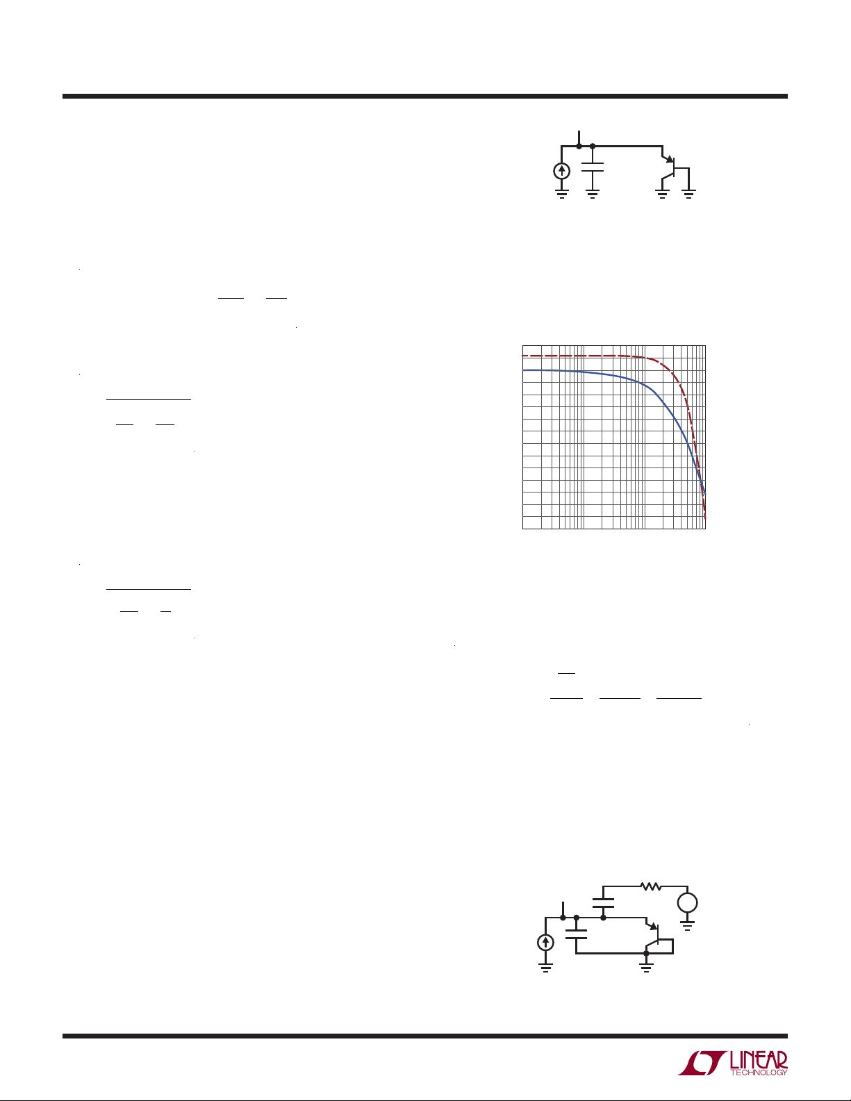
2N3906
10μF
Figure 1.
Q1
AN137 F01
500μA
I
1
The operating point at 500μA gives a DC impedance of
1.27kΩ. The small signal impedance can be plotted in
spice and is 52Ω out to 10MHz.(Solid line is magnitude
of impedance, and dashed line is phase of impedance).
4
AN137 F02
2
0
–2
–4
–6
–8
–10
–12
–14
–16
–18
–20
–22
–24
–26
(DEGREE)
(dB)
34.3
34.2
34.1
34.0
33.9
33.8
33.7
33.6
33.5
33.4
33.3
33.2
33.1
33.0
32.9
100k
10M 100M1M
(Hz)
Figure 2.
The small signal impedance can be calculated as follows:
Now the temperature measurement only depends on the
ideality factor n.
The ideality factor is relatively stable compared to the saturation current. Conceptually, the delta measurement is far
more accurate than the single measurement, because the
delta measurement cancels the saturation current and all
other non-ideal mechanisms not modeled by the equations.
For both cases, the accuracy of temperature measurement depends on the forcing current accuracy, the voltage
measurement accuracy, and relatively noise free signals.
Noise Sources
A typical diode temperature sensor is comprised of a
2N3906, 10μF capacitor, current source, and voltage
measurement.
⎛
⎞
kT
⎜
R
small–signal
⎟
q
⎝
=
26mV
⎠
=
I
C
I
C
26mV
=
500μA
= 52Ω
This implies that fast clock and PWM signals may inject
noise into the measurement if the driving impedance is
close to 52Ω.
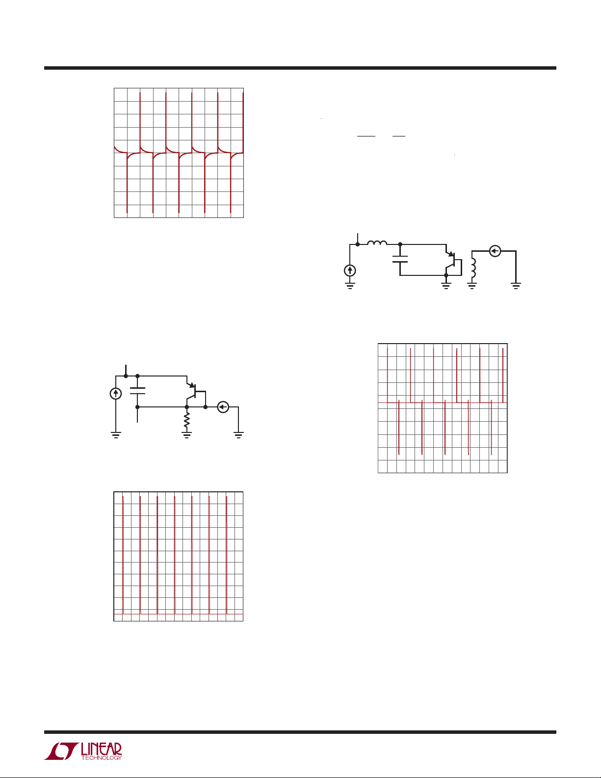
A simulation of a capacitive coupled source shows that
the filter capacitor is quite effective.
R1
1Ω
V1
I
1
500μA
Figure 3. Pulse (0 3.30 10ps 10ps 100ns 2.5μs 10000)
C1
10μF
C2
10nF
2N3906
Q1
+
–
AN137 F03
V1
an137f
AN137-2
Page 3
Application Note 137
672
665
658
651
644
637
(mV)
630
623
616
609
602
0
(ms)
2024681012141618
AN137 F04
Figure 4.
The simulation uses a 10ps 3.3V signal (V1) injected into
the p-n junction (V1) via a 10nF capacitor (C1). Even a
10nF coupled noise source with very fast 10ps edges can
only generate 30mV spikes shown in the simulation plot.
Another source of error comes from ground impedances.
V1
C1
I
1
500μA
REMOTE
GND
Figure 5. Pulse (0 2A 0 10n 10n 100ns 2.5μs 10000)
658
656
654
652
650
648
(mV)
646
644
642
640
638
636
33
2N3906
10μF
Figure 6.
(μs)
Q1
R2
0.01Ω
I
2
AN137 F05
4834 35 36 37 38 39 40 41 42 43 44 45 46 47
AN137 F06
A 2A current and 10mΩ trace results in a 20mV error. A
typical delta V
ΔVBE=
nkT
q
is
D
⎞
⎛
1
⎜
⎝
10
≈ 60mV
⎟
⎠
In
For a 10% duty cycle, this might result in a 2mV DC shift.
A third source of error is a magnetic field and loop. Magnetic
coupling can be modeled as a coupling between inductors.
V1
K L2 L1 0.01
t
L1
10nH
I
1
500μA
C1
10μF
2N3906
Q1
I
2
t
L2
10nH
AN137 F07
Figure 7. Pulse (0.2A 0 10n 10n 1.25μs 2.5μs 10000)
660
655
650
645
640
635
(mV)
630
625
620
615
610
464
(μs)
478466 468 470 472 474 476
AN137 F08
Figure 8.
A 3cm PCB trace over a ground plane can have about
10nH of inductance. If 2A is injected into a parallel trace
and the coupling is 1.0%, 30mV of noise can be generated, possibly causing a DC shift of 3mV.
HOW NOISE AFFECTS MEASUREMENTS
Linear Technology devices typically implement a lowpass
filter, which filters spikes and noise. However, in some
cases filtering results in a significant DC shift.
an137f
AN137-3
Page 4
Application Note 137
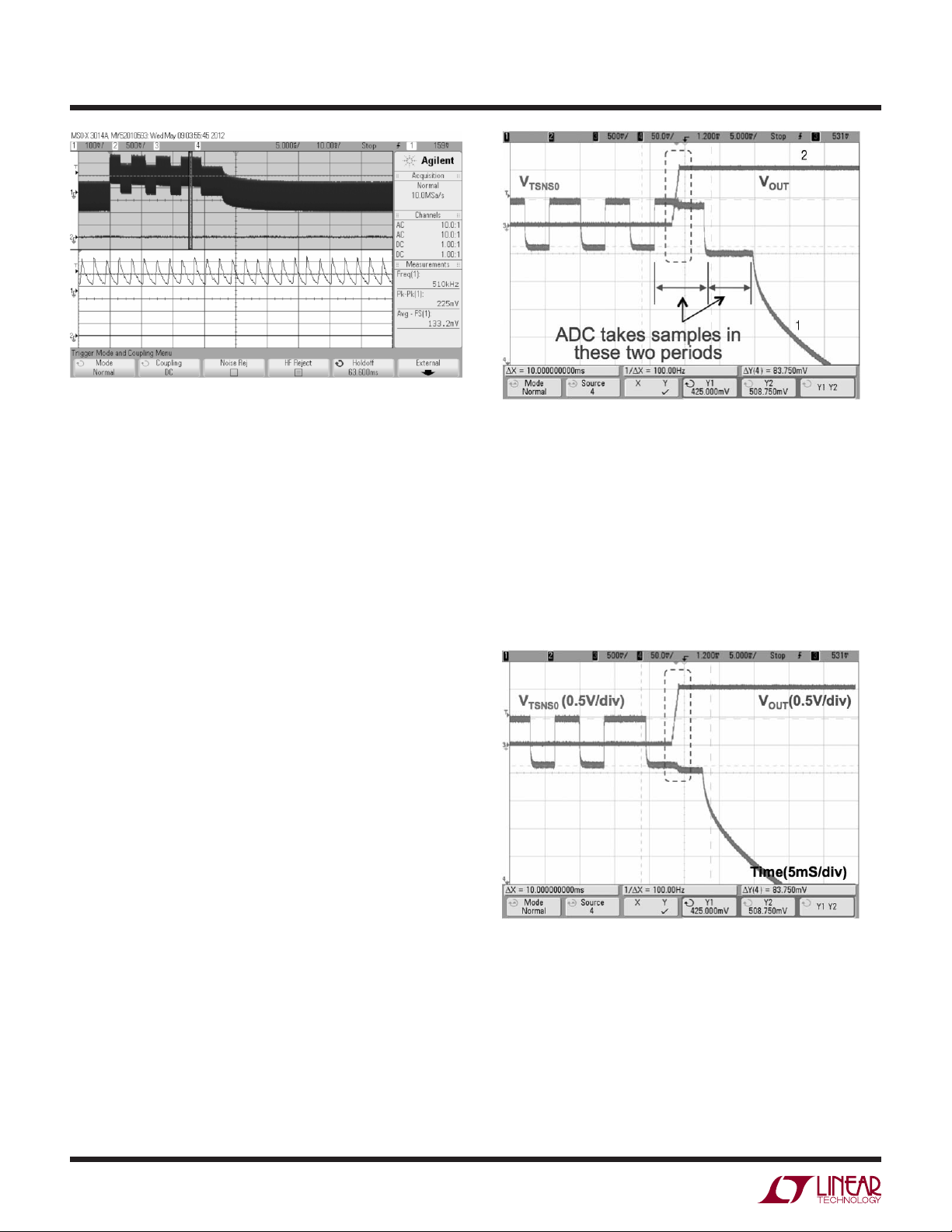
Figure 9.
The example shown in Figure 9, from an LTC3880, shows
an asymmetrical waveform on the TSENSE pin (channel
1) caused by injecting some of the switch node signal into
the TSENSE pin. When this is filtered, it results in a DC
shift. If temperature is calculated using a ΔV
and the DC shift is the same for both V
the effect will be cancelled out. This means that if the
error mechanism is consistent between current measurements, ΔV
is robust. If the single VBE measurement is
BE
used, the DC shift from the filtering will be a source of
measurement error. (LTC3880 does not support single
measurements)
ΔV
BE
calculation,
BE
measurements,
BE
Figure 10.
An Example Coupling Problem
The example shown in Figure 10 comes from an LTC3880.
Signal 1 is the TSENSE signal. When the LTC3880 is applying 32μA, you get the higher signal level, and when it
is applying 2μA, you get the lower signal level. The last
high and low portions of the waveform are where the
two measurements are taken. Signal 2 is the V
OUT
of the
LTC3880, which is coupling into the 32μA measurement.
If the magnitude of noise is very large with respect to ΔV
BE
,
and the noise is asymmetrical (as in the scope shot) and
different between current measurements, ΔV
cannot
BE
cancel out the noise. In this case a single measurement
can produce a more accurate temperature measurement.
For example, suppose noise causes an error of 50mV. A
typical ΔV
single V
Therefore, in systems with systematic noise, the ΔV
is 70mV. The error can be as high as 70%. If a
BE
is used, the error is about 50mV/600mV, or 8%.
D
BE
measurement produces the highest accuracy by eliminating
as a source of error. (See ΔVBE equation). In systems
I
S
with large non-systematic noise, the V
measurement
BE
produces the highest accuracy.
Overall, the best accuracy comes from a good layout that
ensures near zero noise that is systematic, and uses a
calculation.
ΔV
BE
Non-systematic noise sources require good layout because
the ΔV
approach cannot reject them.
BE
Figure 11.
The same coupling can occur in the 2μA measurement as
shown in Figure 11. The asymmetry comes from the fact
that the coupling affects only one of two measurements, so
it is not cancelled by the ΔV
calculation. Furthermore, the
BE
error will appear random because the output turn-on event
and the current forcing mechanism are not synchronized.
The only defense against this error is prevention of the
coupling by proper layout, or widening the fault limits.
an137f
AN137-4
Page 5

Figure 12.
MITIGATING ERROR SOURCES
There are two primary methods of preventing errors, both
require proper PCB layout. The first involves elimination of
shared ground paths. The second involves proper signal
trace routing.
Linear Technology data sheets specify how to return current
from the collector and base of the temperature measurement
transistor to the device. Typically the current returns to a
sense ground (SGND), or an amplifier negative (–) input.
Application Note 137
The current should return to the device via its own sense
trace to ensure there is no shared impedance with high
current paths, and to the data sheet specified pin.
Figure 12 shows a LTC3883 and 2N3906 PNP current
sense. Q10 in circle 1 is the p-n junction temperature
sensor and is filtered by C99. The purpose of C99 is to
provide a low AC impedance to prevent any DC offsets
from rectification or non-linear waveforms, and to keep
coupled noise out of the LTC3883 ADC. The routing uses
two parallel pairs on the same layer so that any coupling
from noise sources becomes a common mode signal
to the ADC in the LTC3883 and are rejected. The anode
trace routes to the sense pin to the LTC3883 Pin 32
shown in circle 2, and the cathode is routed to SGND: the
exposed PAD on the back of the LTC3883. The cathode
routing to the exposed PAD ensures no high current from
the power ground flows through the sense line.
Figure 13 shows an LTC2991 and two 2N3906 PNP
temperature sensors. As in the previous example, capacitor filtering is added near the PNP. However, capacitor filtering was also added at the input of the LTC2991.
Figure 13.
an137f
AN137-5
Page 6

Application Note 137
The longer trace run offers more opportunity to pick up
noise farther from the PNP due to trace inductance. Typically this capacitor is added as an option and installed
only if there is a problem. Additionally, notice that the
routes avoid switching areas by following the edges of
the plane between functional circuits. The routes from
the PNP farthest to the right go right between a LTC3883
buck converter below, and a LT1683 isolated boost above.
NOTE: Linear Technology strongly recommends
Placement of a filter capacitor near the PNP tem-
perature sensor, Routing differentially, and Avoiding
noisy signals. Long routes may pick up more noise,
so optionally add a filter capacitor near the device.
Some designs may use a power block with built in temperature diode. Some of these power blocks do not have
a pin for the low sense of the diode. These blocks may not
have a filter capacitor. In these situations, you can place a
filter on your board as close to the high side diode sense
pin of the power block as possible, and try to minimize all
noise sources. A low sense line can still be routed from the
power ground, but you can’t eliminate the shared current
from the switching path, so some noise will be injected.
You can mitigate some of the problems that may result by:
1. Using a slower V
ramp rate when turning on
OUT
2. Adding an offset to the measurement using the proper
register (digital power device) to lower the measured
temperature
3. Raising the overtemperature fault limit
over temperature. In general, a large ideality factor will not
produce an accurate temperature measurement using the
method. The large ideality factor will lead to larger
ΔV
BE
. Furthermore, VBE may be lower because of differ-
ΔV
BE
ences in I
. This may use less of the dynamic range of
S
the ADC and increase signal to noise ratio. In the case of
a single V
measurement, this will degrade results more.
BE
NOTE: Use a diode connected bipolar transistor rather
than a true diode. If you want to use a diode anyway,
contact Linear Technology for advice on suitability for
the given device.
600
570
V
(V1)
540
510
(mV)
480
450
420
390
360
330
300
270
0
30 40 50 7060 80 90 10010 20
(μA)
V
(V2)
AN137 F14
Figure 14. 2N3906 and IN4148
An LTspice® simulation demonstrates the difference between a diode connected 2N3906 and a 1N4148. The diode
has almost 150mV lower voltage at 30μA.
4. Adding a capacitor on the power block
CHOICE OF P-N JUNCTION DEVICE
Even though a diode can be used to measure temperature,
a diode connected PNP or NPN is preferred. The ideality
factor of a diode is up to twice as large as a diode connected bipolar transistor. Some diodes do not exhibit
increasing ΔV
with temperature, resulting in large errors
BE
AN137-6
(mV)
570
V
(V1)
540
510
480
450
420
390
360
330
300
270
0
70mV
Figure 15. 2N3906 DV
(μA)
2N3906
V
(V2)V(V2)
1N4148
10010 20 30 40 6050 70 80 90
AN137 F15
BE
an137f
Page 7

Application Note 137
The diode-connected transistor shows a typical room
temperature ΔV
(mV)
of 70mV.
BE
570
V
(V1)
540
510
480
450
420
390
360
330
300
270
0
Figure 16. IN4148 ΔV
127mV
(μA)
2N3906
V
(V2)V(V2)
2N4148
10010 20 30 40 6050 70 80 90
AN137 F16
BE
The diode shows a typical room temperature ΔVBE of
127mV. If the part is using a ΔV
measurement, and if
BE
the ADC has a null and diff amp with gain, you must make
certain the device can handle the larger ΔV
BE
.
4. Avoid routing near noise generators such as switch
nodes, large current traces, large transformers, etc.
5. If using a power block, add a filter cap to the block if
possible, or as close as possible to the diode pin if it
can’t be on the power block.
6. Use a power block with two-pin sensing of the diode if
possible.
7. If you have a sub-optimal layout, add offset to the offset
register if one is available, or raise the fault limit. In some
designs you can make these adjustments during turn
on or soft start and restore them during steady state.
APPENDIX A: GENERAL NOISE SOURCES AND
MITIGATION
A more general and analytical approach to noise is offered
based on material from Noise Reduction Techniques in
Electronic Systems, Henry W. Ott. These principles can
guide you in solving problems not directly covered in the
application note.
In all cases, if a diode is used, the controller IC must have
a register for setting the ideality. Some Linear Technology
controller ICs have a register for this and others don’t. The
ones that don’t are typically set for a 2N3904 or 2N3906.
REVIEW OF DESIGN RULES
A simple set of design rules can prevent a lot of problems:
1. Use a diode-connected transistor. Either 2N3904 or
2N3906. Follow recommendations on the data sheet.
2. Place a filter capacitor near the diode (less than a few
millimeters. Add a capacitor near the controller IC if
the transistor is more than a couple of inches away if
there is space.
3. Route a differential connection from the transistor to
the controller IC with minimum spacing whether the
part has a separate -TSENSE pin or not. If not, tie the
low side to the SGND pin. If there is no SGND pin, use
the PGND. Connect at the pin in all cases if possible.
Noise Sources
Conduction: noise on any PCB trace will move noise from
one part of the PCB to another. Generators of voltage
noise are the gate drivers, the switch node, and switching
currents that flow through resistors and inductive traces.
Coupling through Impedance: Any time two currents share
an impedance, the resulting voltage from one current path
is superimposed on the resulting voltage due to the other
current path. Shared current paths include the gate-driveloop/drain-source-loop/temperature-sense-loop.
Coupling through parasitic impedance: PCB traces that
are close together can couple through parasitic capacitance and mutual inductance. Low impedance switching
nodes can couple to higher impedance sense nodes. For
example, a gate drive can couple into a temperature sense
line via stray capacitance, or a switch current can couple
into a temperature sense line via an inductively coupled
parallel trace.
an137f
AN137-7
Page 8

Application Note 137
NOISE MITIGATION
Capacitive Coupling
If a noisy trace is routed next to a sensing trace, the noise
will couple to the sensing trace via capacitance.
C
COUPLING
10p
+
V
NOISE
–
REC
C
REC
6p
R
REC
50Ω
AN137 A1
Figure A1.
The analytical expression of the coupling from Ott is:
V
REC
=
⎡
C
jω
COUPLING
⎢
⎢
C
⎣
COUPLING+CREC
jω+
R
()
RECCCOUPLING+CREC
1
⎤
⎥
⎥
⎦
V
NOISE
(dB)
–10
–20
–30
–40
–50
–60
–70
–80
–90
–100
–110
–120
100
(Hz)
AN137 A2
90.3
90.0
89.7
89.4
89.1
(DEGREE)
88.8
88.5
88.2
87.9
87.6
87.3
87.0
10M1k 10k 100k 1M
Figure A2.
At 500kHz, the noise coupled to the receiver (temp sensor) is 10mV.
If a shield is added, the equivalent circuit looks like this:
+
–
C
COUPLING
10p
V
NOISE
C
SHIELD
100p
REC
C
REC
6p
R
50Ω
REC
In the case where R
is smaller than the impedance
REC
of the two capacitors, the equation can be simplified to:
REC
= jω R
REC CCOUPLING VNOISE
V
To get a sense of magnitude, a simulation of the above
circuit with an input of 5V to represent a gate drive signal,
and 50Ω to represent a temperature sensor, the following
is the frequency response:
AC 5
AN137 A3
Figure A3.
In this case there is no coupling to the receiver at all. An
example of shielding is given in the LTC2991 data sheet
as shown in Figure A4:
GND SHIELD
TRACE
470pF
NPN SENSOR
Figure A4.
LTC2991
V1
V2
V3
V4
V5
V6
V7
V8
V
ADR2
ADR1
ADR0
PWM
SCL
SDA
GND
CC
0.1μF
AN137 A4
In this case, the signals are routed differentially, so the
shield is protecting against capacitive coupling into both
traces. Notice that a portion of the traces is not shielded.
This area must be kept small and away from noise sources.
AN137-8
an137f
Page 9

Application Note 137
The example uses 10pF coupling to give some general
idea of magnitudes of coupling. It is best to make real
estimates of coupling capacitance and calculate the effect.
Also note, that parallel routing does not protect against
capacitive coupling if the low sense is not a high impedance input.
C
COUPLING
10p
+
V
NOISE
–
C1
10p
C
REC
6p
C2
6p
+
REC
R
REC
50Ω
–
R1
REC
10
AN137 A5
Figure A5.
The model in Figure A5 shows capacitive coupling into
both traces.
The frequency response is almost identical to the single
route because the impedance of the negative sense is
almost zero, therefore the noise can’t couple into it to
cancel the high side.
If the impedance on the negative sense is very high, such
as 1M shown in Figure A6:
AN137 A8
99
90
81
72
63
(DEGREE)
54
45
36
27
18
9
0
–9
10M1k 10k 100k 1M
(dB)
–10
–20
–30
–40
–50
–60
–70
–80
–90
–100
–110
–120
100
(Hz)
Figure A8.
(dB)
–10
–20
–30
–40
–50
–60
–70
–80
–90
–100
–110
–120
C
COUPLING
10p
+
V
NOISE
–
C1
10p
C
REC
6p
REC
+
R
50Ω
REC
the attenuation is 80dB at 10kHz.
Therefore, parallel routing would work on an LTC2991
current/temperature monitor, which has ± high impedance inputs, but would not work on an LTC3880 family
AC 5
C2
6p
Figure A6.
R1
1M
REC
–
AN137 A6
digital power buck converter which has a low impedance
minus input.
1
One last note: looking at the coupling equation:
V
If R
= jωR
REC
REC
REC CCOUPLING VNOISE
is reduced, so is the coupled noise. Adding a
capacitor to the input of the receiver will lower the AC
impedance. The simulation of this is left to the reader.
Inductive Coupling
Inductive coupling occurs when high currents flow through
a trace, creating a magnetic field, and the field enters the
current loop of another circuit. The current loop will have
a series voltage noise source from the external field.
REC
= jωMI
V
100
(Hz)
AN137 A7
89.6
89.2
88.8
88.4
(DEGREE)
88.0
87.6
87.2
86.8
86.4
86.0
85.6
10M1k 10k 100k 1M
Figure A7.
Note 1: Parallel routing will still eliminate shared current coupling from
power ground
an137f
AN137-9
Page 10

Application Note 137
inductance and current. For example:
L
COUPLING1
20n
K1 L
+
V1
–
COUPLING1 LCOUPLING2 0.5
L
COUPLING2
20n
REC
t
t
AC 5
R
SENSOR
50Ω
R
1M
Figure A9.
Suppose the noise source is 5V, like a gate driver, driving
15Ω, which is about 300mA, similar to a typical gate driver.
This couples into a 50Ω sensor that drives an amplifier
input with 1M input impedance.
–10
–20
–30
–40
–50
–60
(dB)
–70
–80
–90
–100
–110
–120
100
(Hz)
Figure A10.
This will produce about 10mV at the receiver at 500kHz,
(shown in Figure A10) a value similar to the capacitive
coupling example.
The trace length causes the inductance, but the mutual inductance (represented as coupling factor in the simulation)
causes the coupling. The mutual inductance is proportional
to the area of the loop with the sensor and receiver.
REC
AN137 A10
10M1k 10k 100k 1M
R1
15Ω
AN137 A9
89.5
90.0
90.5
91.0
91.5
92.0
92.5
93.0
93.5
94.0
94.5
95.0
(DEGREE)
Suppose the coupling was reduced to 0.05:The received noise voltage is proportional to the mutual
AN137 A11
89.5
90.0
90.5
91.0
91.5
(DEGREE)
92.0
92.5
93.0
93.5
94.0
94.5
95.0
10M1k 10k 100k 1M
(dB)
–30
–40
–50
–60
–70
–80
–90
–100
–110
–120
–130
–140
100
(Hz)
Figure A11.
The result is a 20dB improvement, or 1mV of coupled
noise at 500kHz (shown in Figure A11).
There are several ways to make the loop smaller. The high
side sense can be routed over a ground plane. This will
only help at high frequencies because at low frequencies
the current will take the shortest path through the ground
plane, which will not be under the trace. Furthermore, the
shared ground may cause coupling, which is discussed
in the next section.
The high side and low side of the sensor can be routed
as parallel traces as close together as possible. As long
as the current only flows through the low side sense and
not an alternate ground path, this will make the loop area
very small. If there is an alternate ground path, the current
will only flow through the low sense line if the frequency
is high. Most situations allow this routing except some
power blocks discussed in the main portion of the application note.
Also, a shield may be added around the parallel traces.
Shields may be grounded at either end, so this must be
considered. Ott gave experimental data that will aid intuition in deciding how to ground the low sense and shield.
AN137-10
an137f
Page 11

Application Note 137
AN137 A12
Figure A12.
The data in Figure A12 applies shielding and routing where
the low sense is grounded at the sensor and receiver. This
applies to the case where a power block is used and the
low sense cannot be removed from the power ground
return signal. Assume the sensor is the 100Ω resistor,
and the receiver is the 1M resistor.
Case C represents routing the high and low sense in parallel
with minimal spacing (low sense on both sides, and with
low sense a ground), with a ground plane in parallel as the
alternate path. Case F represents Case C with an additional
shield. The minor difference in attenuation suggests that
Case C is the better choice because routing is simpler.
Case D represents a simple parallel routing, again with
the low sense a ground.
This shows that the traditional parallel sense traces can
be improved by routing the low sense (ground) on both
sides of the high sense and grounding at both ends. This
would apply to a power block when the low sense is tied
to power ground in the module.
AN137 A13
Figure A13.
Things are better when it is possible to ground at only
one end.
As in the previous cases, the sensor is the 100Ω resistor,
and the receiver is the 1M resistor. Case H represents the
traditional parallel close routing. This is more than 15dB
better than the previous case where you are forced to
ground both ends.
Case G represents routing the low sense (ground) on
both sides of the high sense. This is more than 50dB
better than Case C and 25dB better than Case H. This
is even 10dB better than Case I, which was the example
from LTC2991 used in the capacitive coupling section.
However, the LTC2991 low sense is high impedance and
not ground as in this example. Therefore, don’t disregard
the LTC2991 data sheet.
55dB would be 8mV for a 5V noise source. 80dB would
be 0.5mV for a 5V noise source. This is not an apples to
apples comparison, as the experimental data was taken at
50kHz. However, the principles are clear. If you have the
space, consider routing the low sense/ground on both
sides of the high sense.
Information furnished by Linear Technology Corporation is believed to be accurate and reliable.
However, no responsibility is assumed for its use. Linear Technology Corporation makes no representation that the interconnection of its circuits as described herein will not infringe on existing patent rights.
an137f
AN137-11
Page 12

Application Note 137
Ground Coupling
Grounding loops are not typically the first source of noise
coupling. However, if a sensor low sense is grounded at
both ends, as when using a power block, a ground loop
is formed. This loop can receive a magnetic field, hence
inductive coupling, as discussed in the previous section.
Not much can be done about this other than to make the
shortest low sense route possible back to the receiver,
and keep the layers between the trace and ground plane
as thin as possible.
A more serious problem are share ground paths where one
path contains high current. While it is possible to design
a DC/DC converter using a parallel ground system (all
loops have separate routes to the PGND pin), it is not typically done because at high switching frequencies ground
signals will have inductive and capacitive coupling. The
typical grounding system is a multipoint ground, almost
always a ground plane, or a couple of very large plane
sections that attempt to separate the gate loop from the
power path loop.
For sensing, the main concern is allowing sensor low
sense current to share any of these paths. If the singled
grounded shielding is used, then the high current grounds
are avoided. If a power block is used, current will be shared
on the module and its ground pin. The best you can do
is route the low sense from the module ground pin to
minimize the shared path.
Most devices will have two grounds that are connected at
a single point. One will be called signal ground, and one
power ground. The shield used to prevent capacitive and
inductive grounding is always tied to the signal ground.
This prevents a shared ground path at the device end of
the sensor connection.
Therefore, the worst scenario is a power block without a
low sense pin, with a device that only has a power ground.
The best case is a sensor with access to both high and
low sense, where the low sense is not grounded, and the
device has a signal ground and a power ground. Controlling
these cases has to be done early in the design process
during component selection, long before layout.
AN137-12
Linear Technology Corporation
1630 McCarthy Blvd., Milpitas, CA 95035-7417
(408) 432-1900 ● FAX: (408) 434-0507
●
www.linear.com
an137f
LT 0912 • PRINTED IN USA
© LINEAR TECHNOLOGY CORPORATION 2012
 Loading...