

Page 1
Application Note 128
2 Nanosecond, 0.1% Resolution Settling Time
Measurement for Wideband Amplifiers
Quantifying Quick Quiescence
Jim Williams
June 2010
INTRODUCTION
Instrumentation, waveform synthesis, data acquisition,
feedback control systems and other application areas utilize wideband amplifiers. Current generation components
(see box section, page 2, “A Precision Wideband Amplifier
with 9ns Settling Time”) feature good DC precision while
maintaining high speed operation. Verifying precision
operation at high speed is essential, and presents a high
order measurement challenge.
SETTLING TIME DEFINED
Amplifier DC specifications are relatively easy to verify.
Measurement techniques are well understood, albeit
often tedious. AC specifications require more sophisticated approaches to produce reliable information. In
particular, amplifier settling time is extraordinarily difficult
to determine. Settling time is the elapsed time from input
application until the output arrives at and remains within
a specified error band around the final value. It is usually
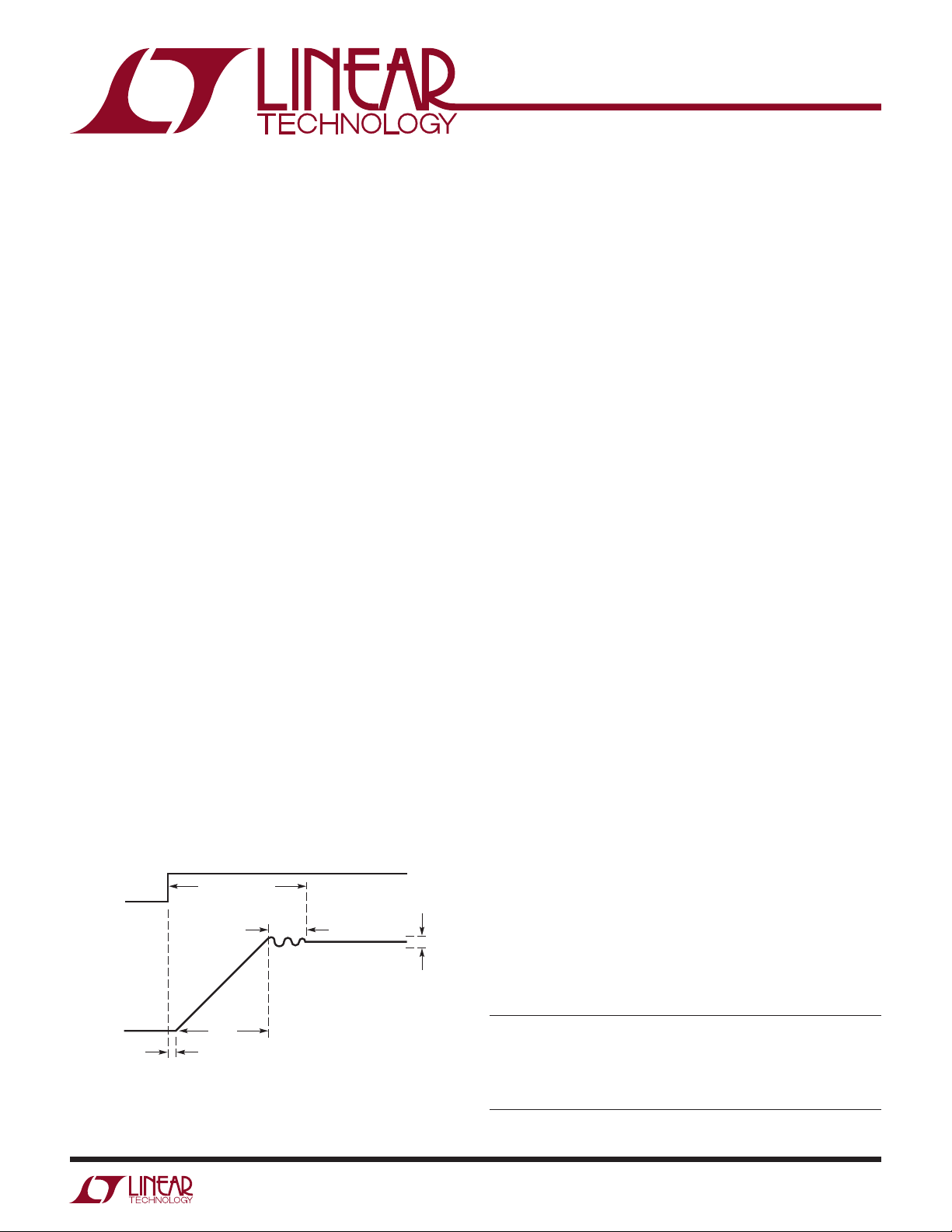
specified for a full-scale transition. Figure 1 shows that
settling time has three distinct components. The delay time
is small and almost entirely due to amplifier propagation
delay. During this interval there is no output movement.
SETTLING TIME
INPUT
RING TIME
During slew time the amplifier moves at its highest pos-
sible speed towards the final value. Ring time defines the
region where the amplifier recovers from slewing and
ceases movement within some defined error band. There
is normally a trade-off between slew and ring time. Fast
slewing amplifiers generally have extended ring times,
complicating amplifier choice and frequency compensation.
Additionally, the architecture of very fast amplifiers usually
1
dictates trade-offs which degrade DC error terms
.
Measuring anything at any speed requires care. Dynamic
measurement is particularly challenging. Reliable nanosecond region settling time measurement constitutes a
high order difficulty problem requiring exceptional care
2
in approach and experimental technique
.
CONSIDERATIONS FOR MEASURING NANOSECOND
REGION SETTLING TIME
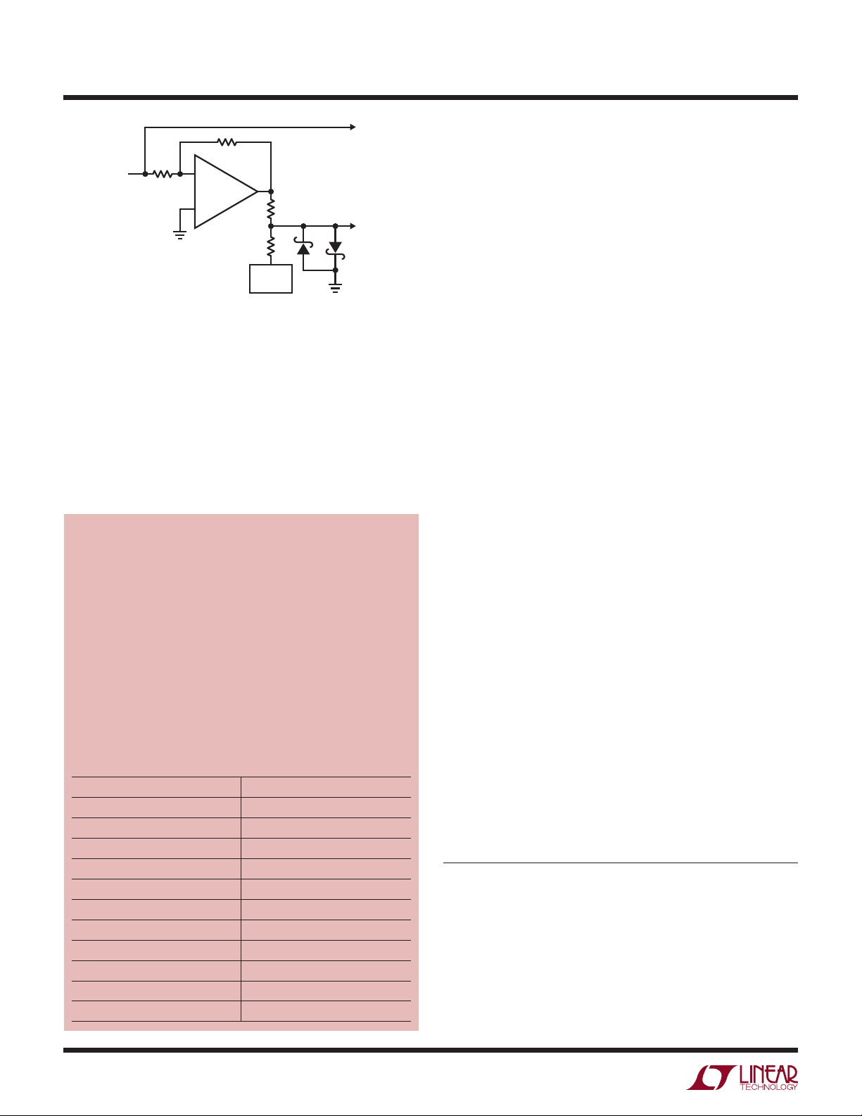
Historically, settling time has been measured with circuits
similar to that in Figure 2. The circuit uses the “false sum
node” technique. The resistors and amplifier form a bridge
type network. Assuming ideal resistors, the amplifier output
will step to –V
when the input is driven. During slew,
IN
the settle node is bounded by the diodes, limiting voltage
excursion. When settling occurs, the oscilloscope probe
voltage should be zero. Note that the resistor divider’s
attenuation means the probe’s output will be one-half of
the actual settled voltage.
ALLOWABLE
OUTPUT
ERROR
OUTPUT
Figure 1. Settling Time Components Include Delay, Slew and
Ring Times. Fast Amplifiers Reduce Slew Time, Although
Longer Ring Time Usually Results. Delay Time Is Normally a
Small Term
SLEW
TIME
DELAY TIME
BAND
AN128 F01
In theory, this circuit allows settling to be observed to
small amplitudes. In practice, it cannot be relied upon to
produce useful measurements. Several flaws exist. The
Note 1. This issue is treated in detail in latter portions of the text. Also see
Appendix B, “Practical Considerations for Amplifier Compensation”.
Note 2. The approach used for settling time measurement and its
description, while new, borrows from previous publications. See
References 1-5, and Reference 9.
L, LT, LTC, LTM, Linear Technology and the Linear logo are registered trademarks of Linear
Technology Corporation. All other trademarks are the property of their respective owners.
an128f
AN128-1
Page 2
Application Note 128
INPUT STEP TO
OSCILLOSCOPE
POSITIVE INPUT
FROM PULSE
GENERATOR
Figure 2. Popular Summing Scheme for Settling Time
Measurement Provides Misleading Results. Pulse Generator
Post-Transition Aberrations Appear at Output. Large Oscilloscope
Overdrive Occurs. Displayed Information Is Meaningless
–
AMPLIFIER
+
R
R
+V
REF
OUTPUT TO
OSCILLOSCOPE
AN128 F02
circuit requires the input pulse to have a flat top within the
required measurement limits. Typically, settling within 5mV
or less for a 5V step is of interest. No general purpose pulse
generator is meant to hold output amplitude and noise within
these limits. Generator output-caused aberrations appearing at the oscilloscope probe will be indistinguishable from
A PRECISION WIDEBAND AMPLIFIER WITH 9ns
SETTLING TIME
Historically, wideband amplifiers provided speed, but
sacrificed precision and, often, settling time. The LT1818
op amp does not require this compromise. It features
low offset voltage and bias current with adequate gain
for 0.1% accuracy. Settling time is 9ns to 0.1% for a
5V step. The output will drive a 100 load to ±3.75V
with ±5V supplies, and up to 20pF capacitive loading
is permissible at unity gain. The table below provides
short form specifications.
LT1818 Short Form Specifications
CHARACTERISTIC SPECIFICATION
Offset Voltage 0.2mV
Offset Voltage vs Temperature 10µV/°C
Bias Current 2µA
DC Gain 2500
Noise Voltage 6nV/√Hz
Output Current 70mA
Slew Rate 2500V/µs
Gain-Bandwidth 400MHz
Delay 1ns
Settling Time 9ns/0.1%
Supply Current 9mA
amplifier output movement, producing unreliable results.
The oscilloscope connection also presents problems. As
probe capacitance rises, AC loading of the resistor junction
influences observed settling waveforms. 1x probes are not
suitable because of their excessive input capacitance. A 10x
probe’s attenuation sacrifices oscilloscope gain and its 10pF
capacitance still introduces significant lag at nanosecond
speeds. An active 1x, 1pF FET probe largely alleviates the
problem but a more serious issue remains.
The clamp diodes at the settle node are intended to reduce
swing during amplifier slewing, preventing excessive oscilloscope overdrive. Unfortunately, oscilloscope overdrive
recovery characteristics vary widely among different types
and are not usually specified. The Schottky diodes’ 400mV
drop means the oscilloscope will undergo an unacceptable
3
overload, bringing displayed results into question
.
At 0.1% resolution (5mV at the amplifier output –2.5mV at
the oscilloscope), the oscilloscope typically undergoes a
10x overdrive at 10mV/DIV, and the desired 2.5mV baseline
is unattainable. At nanosecond speeds, the measurement
becomes hopeless with this arrangement. There is clearly
no chance of measurement integrity.
The preceding discussion indicates that measuring amplifier settling time requires an oscilloscope that is somehow
immune to overdrive and a “flat top” pulse generator. These
become the central issues in wideband amplifier settling
time measurement.
The only oscilloscope technology that offers inherent
4
overdrive immunity is the classical sampling ‘scope
.
Unfortunately, these instruments are no longer manufactured (although still available on the secondary market).
It is possible, however, to construct a circuit that borrows
the overload advantages of classical sampling ‘scope
technology. Additionally, the circuit can be endowed with
features particularly suited for measuring nanosecond
range settling time.
Note 3. For a discussion of oscilloscope overdrive considerations, see
Appendix C, “Evaluating Oscilloscope Overdrive Performance”.
Note 4. Classical sampling oscilloscopes should not be confused with
modern era digital sampling ‘scopes that have overdrive restrictions.
See Appendix C, “Evaluating Oscilloscope Overload Performance” for
comparisons of various type ‘scopes with respect to overdrive. For
detailed discussion of classical sampling ‘scope operation, see References
23-26 and 29-31. Reference 24 is noteworthy; it is the most clearly
written, concise explanation of classical sampling instruments the author
is aware of—a 12-page jewel.
an128f
AN128-2
Page 3
Application Note 128
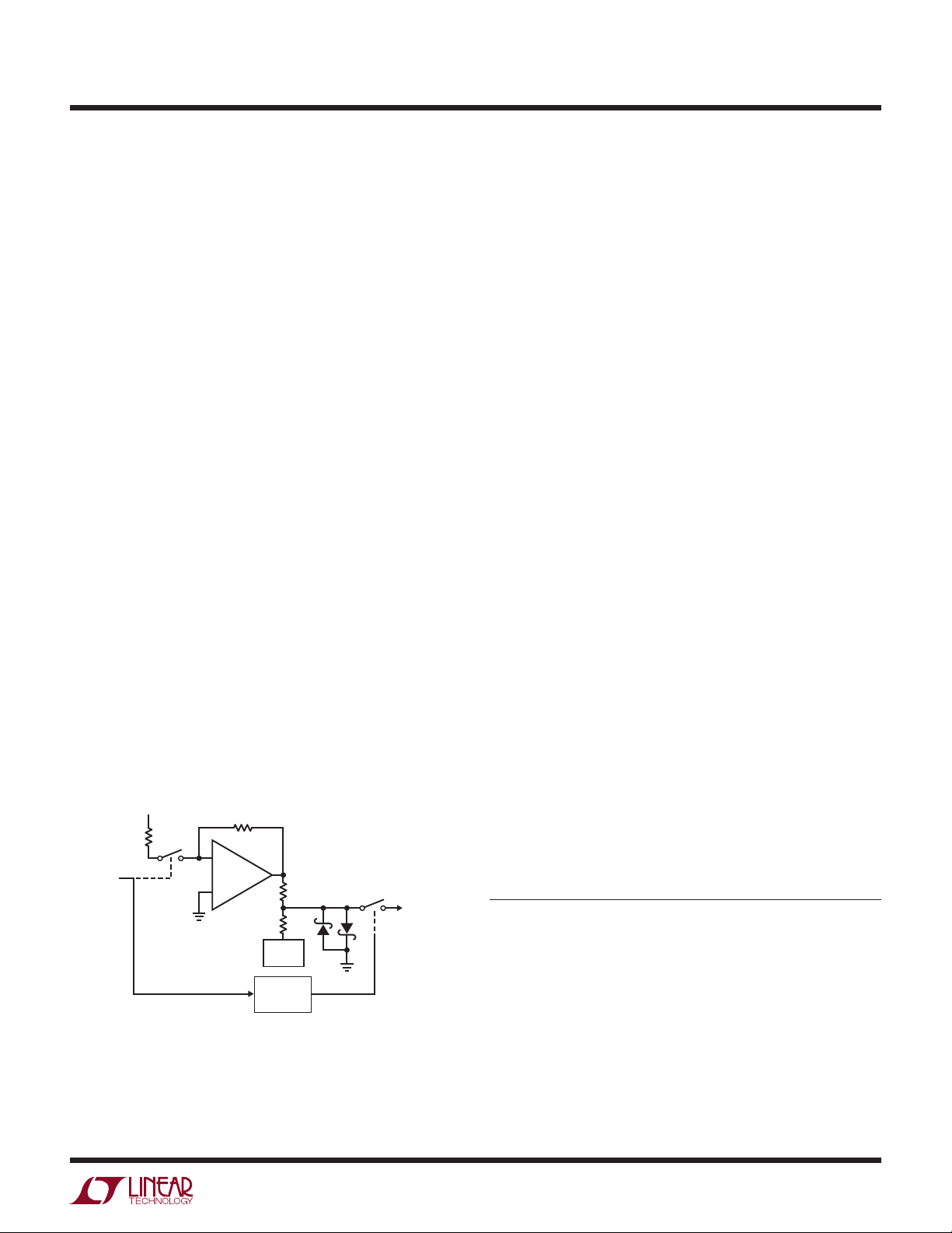
The flat-top pulse generator requirement can be avoided by
switching current, rather than voltage. It is much easier to
gate a quickly settling current into the amplifier’s summing
node than to control a voltage. This makes the input pulse
generator’s job easier, although it still must have a rise time
of about 1 nanosecond to avoid measurement errors.
PRACTICAL NANOSECOND SETTLING TIME
MEASUREMENT
Figure 3 is a conceptual diagram of a settling time measurement circuit. This figure shares attributes with Figure 2,
although some new features appear. In this case, the
oscilloscope is connected to the settle point by a switch.
The switch state is determined by a delayed pulse generator, which is triggered from the input pulse. The delayed
pulse generator’s timing is arranged so that the switch
does not close until settling is very nearly complete. In
this way, the incoming waveform is sampled in time, as
well as amplitude. The oscilloscope is never subjected to
overdrive—no off-screen activity ever occurs.
A switch at the amplifier’s summing junction is controlled
by the input pulse. This switch gates current to the amplifier
via a voltage-driven resistor. This eliminates the “flat-top”
pulse generator requirement, although the switch must
be fast and devoid of drive artifacts.
Figure 4 is a more complete representation of the settling
time scheme. Figure 3’s blocks appear in greater detail and
some new refinements show up. The amplifier summing
area is unchanged. Figure 3’s delayed pulse generator has
+V
CURRENT
SWITCH
INPUT FROM
PULSE
GENERATOR
Figure 3. Conceptual Arrangement Is Insensitive to Pulse
Generator Aberrations and Eliminates Oscilloscope Overdrive.
Input Switch Gates Current Step to Amplifier. Second Switch,
Controlled by Delayed Pulse Generator, Prevents Oscilloscope
from Monitoring Settle Node Until Settling Is Nearly Complete
–
AMPLIFIER
+
SETTLE
NODE
+V
REF
DELAYED
PULSE
GENERATOR
SWITCH
AN128 F03
OUTPUT TO
OSCILLOSCOPE
been split into two blocks; a delay and a pulse generator,
both independently variable. The input step to the oscilloscope runs through a section that compensates for the
propagation delay of the settling time measurement path.
Similarly, another delay compensates sample gate pulse
generator propagation delay. This delay causes the sample
gate pulse generator to be driven with a phase-advanced
version of the pulse which triggers the amplifier under test.
This considerably improves minimum measurable settling
time by making sample gate pulse generator propagation
delay irrelevant.
The most striking new aspects of the diagram are the diode
bridge switch and the multiplier. The diode bridge’s balance, combined with matched, low capacitance Schottky
diodes and high speed drive, yields clean switching. The
bridge switches current into the amplifier’s summing point
very quickly, with settling inside a nanosecond . The diode
clamp to ground prevents excessive bridge drive swings
and ensures that non-ideal input pulse characteristics are
nearly irrelevant.
Requirements for Figure 4’s sample gate are stringent.
It must faithfully pass wideband signal path information
without introducing alien components, particularly those
deriving from the switch command channel (“sample
5
gate pulse”)
.
The sample gate multiplier functions as a wideband, high
resolution, extremely low feedthrough switch. The great
advantage of this approach is that the switch control
channel can be maintained in-band; that is, its transition
rate is held within the multipliers 250MHz bandpass. The
multipliers wide bandwidth means the switch command
transition is under control at all times. There are no outof-band responses, greatly reducing feedthrough and
parasitic artifacts.
Note 5. Conventional choices for the sample gate switch include FET’s
and the sampling diode bridge. FET parasitic gate to channel capacitances
result in large gate drive originated feedthrough into the signal path. For
almost all FETs, this feedthrough is many times larger than the signal to
be observed, inducing overload and obviating the switches’ purpose. The
diode bridge is better; its small parasitic capacitances tend to cancel and
the symmetrical, differential structure results in very low feedthrough.
Practically, the bridge requires DC and AC trims and complex drive and
support circuitry. LTC Application Note 74, “Component and Measurement
Advances Ensure 16-bit DAC Settling Time” utilized such a sampling
bridge and it is detailed in that text. See Reference 3. References 2, 9 and
11 describe a similar sampling bridge based approach.
an128f
AN128-3
Page 4
Application Note 128
TIME-CORRECTED
INPUT STEP TO
OSCILLOSCOPE
SAMPLE
GATE
Y
X
X
SAMPLE
GATE
PULSE
OUTPUT TO
OSCILLOSCOPE
W
SETTLE NODE
2
X • Y = W
PULSE
GENERATOR
INPUT
SAMPLE GATE
PULSE GENERATOR
DELAY COMPENSATION
CURRENT
SWITCH
+V
–
+
–V
SAMPLE GATE PULSE GENERATOR
VARIABLE
DELAY
AMPLIFIER
UNDER TEST
VARIABLE WIDTH
PULSE GENERATOR
SIGNAL PATH
DELAY COMPENSATION
SETTLE
NODE
R
R
+V
REF
SAMPLE GATE
DRIVER
s1
AN128 F04
Figure 4. Block Diagram of Settling Time Measurement Scheme. Diode Bridge Cleanly Switches Input Current to Amplifier. Multiplier
Based Sampling “Switch” Eliminates Signal Paths Pre-Settling Excursion, Preventing Oscilloscope Overdrive. Input Step Time
Reference and Sample Gate Pulse Generator Are Compensated for Test Circuit Delays
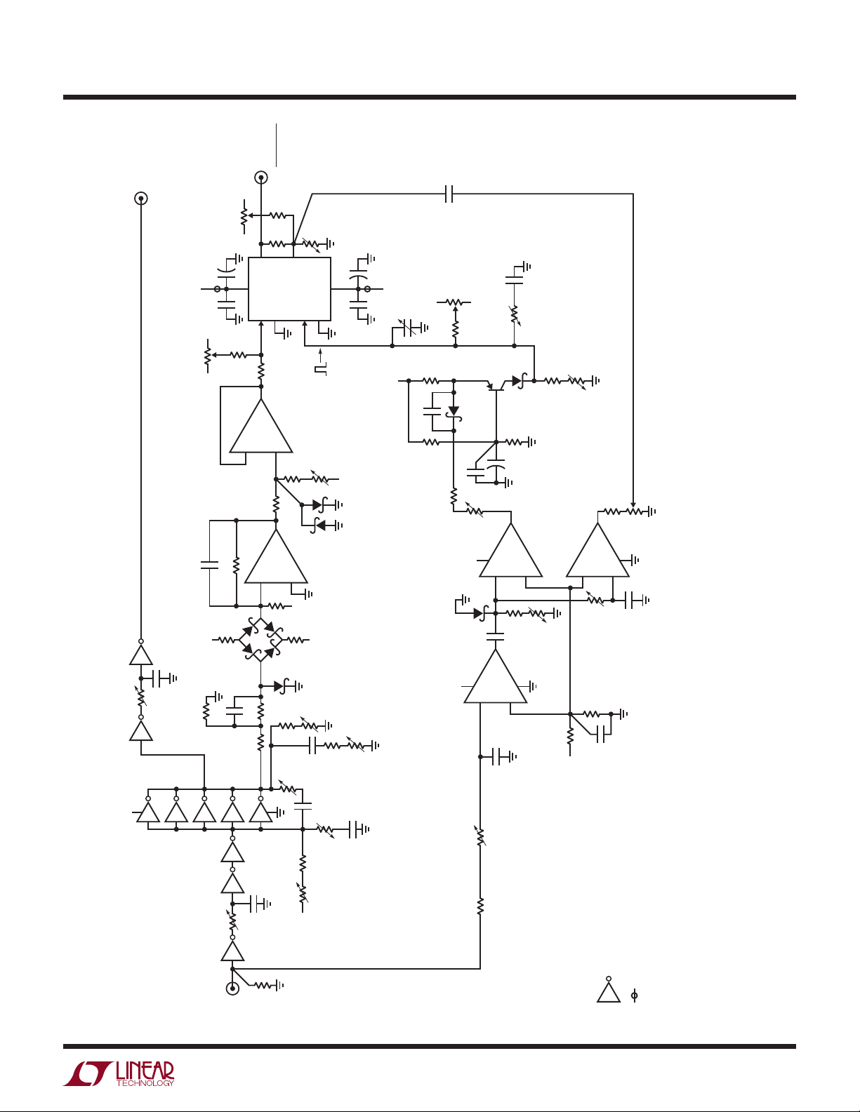
DETAILED SETTLING TIME CIRCUITRY
Figure 5 is a detailed schematic of the settling time measurement circuitry. The input pulse switches the input
bridge via a delay network (“A” inverters) and a driver
stage (“C” inverters). The delay compensates the sample
gate pulse generator’s delayed response, ensuring that
the sample gate pulse can occur immediately after the
amplifier-under-tests’ slew time ends. The delay range is
chosen so that the sample gate pulse can be adjusted to
occur before the amplifier slews. This capability is obviously unused in operation although it guarantees that the
settling interval will always be capturable.
The “C” inverters form a non-inverting driver stage to
switch the diode bridge. Various trims optimize driver
output pulse shape, providing a clean, fast impulse to the
6
diode bridge
. The high fidelity pulse, devoid of undamped
components, prevents radiation and disruptive ground
currents from degrading the measurement noise floor.
The driver also activates the “B” inverters, which supply
a time corrected input step to the oscilloscope.
The driver output pulse transitions through the 1N5712
diode clamp potential in under a nanosecond, causing
essentially instantaneous diode bridge switching. The
resultant cleanly settling current into the amplifier under
tests’ summing point causes proportionate amplifier output
movement. The negative bias current at the amplifiers
summing point combined with the current step produces a
+2.5V to –2.5V amplifier output transition. The amplifier’s
output is compared against a 5V supply derived reference
via the summing resistors. The clamped “settle node” is
unloaded by A1, which feeds the sample gate signal path
information.
The comparator based sample gate pulse generator produces a delayed (controllable by the 20k potentiometer)
pulse whose width (controllable by the 2k potentiometer)
sets sample gate on-time. The Q1 stage forms the sample
gate pulse into a fast rise, exceptionally clean event, furnishing high purity, calibrated amplitude, “on-off” switching
instruction to the sample gate multiplier. If the sample gate
pulse delay is set appropriately, the oscilloscope will not
see any input until settling is nearly complete, eliminating
overdrive. The sample window width is adjusted so that
all remaining settling activity is observable. In this way,
the oscilloscope’s output is reliable and meaningful data
may be taken.
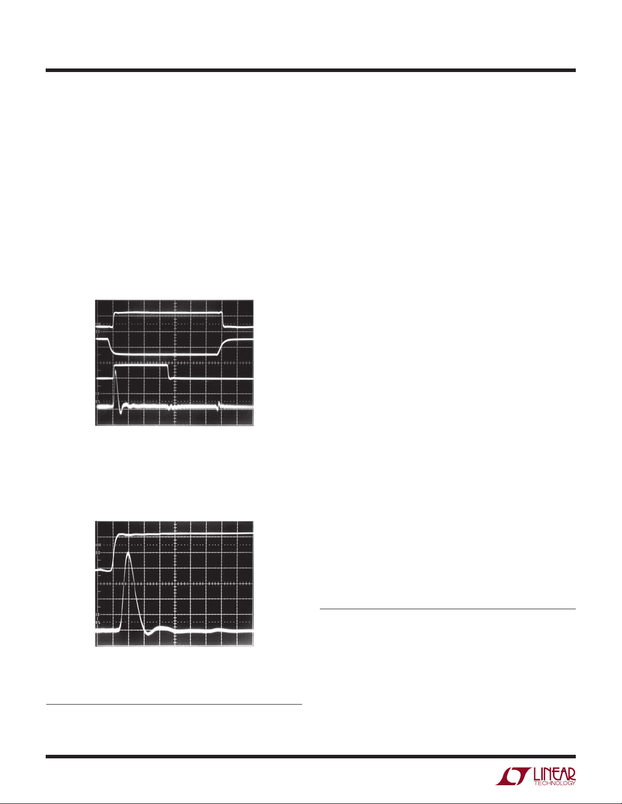
Figure 6 shows circuit waveforms. Trace A is the time-corrected input pulse, Trace B the amplifier output, Trace C the
Note 6. To maintain text flow and focus, trimming procedures are not
presented here. Detailed trimming information appears in Appendix
A, “Measuring and Compensating Settling Circuit Delay and Trimming
Procedures.”
an128f
AN128-4
Page 5
+5
SETTLE
NODE
PULSE
INPUT
AN128 F05
1k*
2k*
200
453*
130
43
200
82
2pF
499*
C
F
, SELECT 1pF TO 8pF
(SEE APPENDIX B)
453*
TIME-CORRECTED
INPUT STEP TO
OSCILLOSCOPE
ALL TRIMMING PROCEDURES DETAILED IN APPENDIX A.
* = 1% METAL FILM RESISTOR
** = HSMS-2860, MATCHED 1 MILLIVOLT AT 10mA
= 1/6 74AHC04. LETTER; e.g. “A”, “B”, “C” DENOTES
SEPARATE PACKAGE. GROUND ALL UNUSED INPUTS.
= FERRITE BEAD, FERRONICS #21-11OJ.
INPUT 50 TERMINATION MUST BE IN-LINE COAXIAL TYPE—DO NOT USE BOARD MOUNTED RESISTOR.
+5V AND –5V SUPPLIES DERIVED FROM BOARD MOUNTED REGULATORS. LT1175 = –5V, LT1761 = 5V.
TRIM BOTH SUPPLIES—0.1%.
BYPASSING NOT SHOWN EXCEPT FOR AD835. BYPASS EACH IC AND INDICATED SUPPLY POINTS WITH
10µF SANYO OSCON PARALLELED WITH 0.1µF FILM CAPACITOR.
SAMPLE GATE
DRIVER
CURRENT
SWITCH
+5V
CURRENT
SWITCH
DRIVER
SCALE
FACTOR
–5V
–
+
SAMPLE GATE PULSE GENERATOR
SAMPLE GATE
SIGNAL PATH DELAY COMPENSATION (8.6ns)
SAMPLE GATE
PULSE GENERATOR PATH
DELAY COMPENSATION (15ns)
Z
W
X
+V
–V
–5
+5
–5
+5
AD835
Y1X1Y2
X2
LT1818
+
–
1/2
LT1720
C2
–
+
LT1818
A1
AMPLIFIER
UNDER TEST
HSMS-2860
2s
HSMS-2860**
4s
OUTPUT TO
OSCILLOSCOPE
SETTLE NODE
1.5
47
1k
PULSE
TOP SMOOTHING
1pF
SAMPLE
GATE
PULSE
SETTLE
NODE
ZERO
1k
1.5k*
50
SEE NOTES
150
500
TOP
FRONT
CORNER
+5
+5
+5
1k*
–5
0.1µF 4.7µF
1pF
0.1µF 4.7µF
2pF TO 10pF
EDGE TIME
10pF
1pF
+5 –5
10k
Y OFFSET
1k
X OFFSET
1k
12pF
10k
1k
DELAY
B
B
+5
CX5
+5
C
AA
1k
DELAY
1k
5pF
20pF
20pF
100
BOTTOM
FRONT
CORNER
TOP
FRONT
CORNER
TOP
REAR
CORNER
24pF
15pF
82
100
BOTTOM REAR
CORNER-TRAILING
ABBERATIONS
IN5711
Q1
2N4260
IN5712
20
1.6k*
3.4k* 261*
2k*
100
SAMPLE GATE
PULSE AMPLITUDE
100
FRONT
CORNER
PURITY
IN5711
0.1µF
82pF
+5
0.1µF
47µF
20
2k*
1k
+
–
1/2
LT1720
C1
+
–
1/2
LT1720
C3
IN5711
1k
2k
SAMPLE
WINDOW WIDTH
50ns TO 110ns
20k
SAMPLE
WINDOW DELAY
9ns TO 150ns
2.5k
FEEDTHROUGH
COMPENSATION
TIME PHASE
100
FEEDTHROUGH
COMPENSATION
AMPLITUDE
+
+
+
–5 +5
OUTPUT
OFFSET
1k
X • Y = W
16k
392
Application Note 128
Figure 5. Detailed Schematic of Settling Time Measurement Circuitry Follows Block Diagram. Trimmed, Paralleled Logic Inverters Provide High Speed Drive to
Current Switch Bridge. Additional Inverters Form Delay Compensation Networks for Signal Path and Sample Gate Pulse Generator. Transistor Stage Shapes Edges and
Amplitude of Sample Gate Pulse Supplied to Multiplier. Multiplier, Functioning as Sample Gate, Passes Settling Time Signal when Sample Gate Pulse Is High
an128f
AN128-5
Page 6
Application Note 128
7
sample gate pulse and Trace D the settling time output
When the sample gate pulse goes high, the sample gate
switches cleanly, and the last 20mV of slew are easily observed. Ring time is also clearly visible, and the amplifier
settles nicely to final value. When the sample gate pulse
goes low, the sample gate switches off with only 2mV of
feedthrough. Note that there is no off-screen activity at any
time—the oscilloscope is never subjected to overdrive.
Figure 7 expands vertical and horizontal scales so that
8
settling detail is more visible
. Trace A is the time-corrected input pulse and Trace B the settling output. The
last 50mV of slew are easily observed, and the amplifier
settles inside 5mV (0.1%) in 9 nanoseconds when CF (see
9
Figure 5) is optimized
A = 5V/DIV
B = 5V/DIV
C = 5V/DIV
D = 10mV/DIV
Figure 6. Settling Time Circuit Waveforms Include TimeCorrected Input Pulse (Trace A), Amplifier-Under-Test Output
(Trace B), Sample Gate (Trace C) and Settling Time Output
(Trace D). Sample Gate Window’s Delay and Width Are
Variable. Trace B Appears Time Skewed Relative to Time
Corrected Trace A.
.
HORIZ = 20ns/DIV
AN128 F06
.
USING THE SAMPLING-BASED SETTLING TIME CIRCUIT
In general, it is good practice to walk the sampling window
“backwards” in time up to the last 50mV or so of amplifier slewing so that the onset of ring time is observable
without encountering oscilloscope overdrive. The sampling based approach provides this capability and it is a
very powerful measurement tool. Slower amplifiers may
require extended delay and/or sampling window times,
necessitating larger capacitor values in the delayed pulse
generator timing networks.
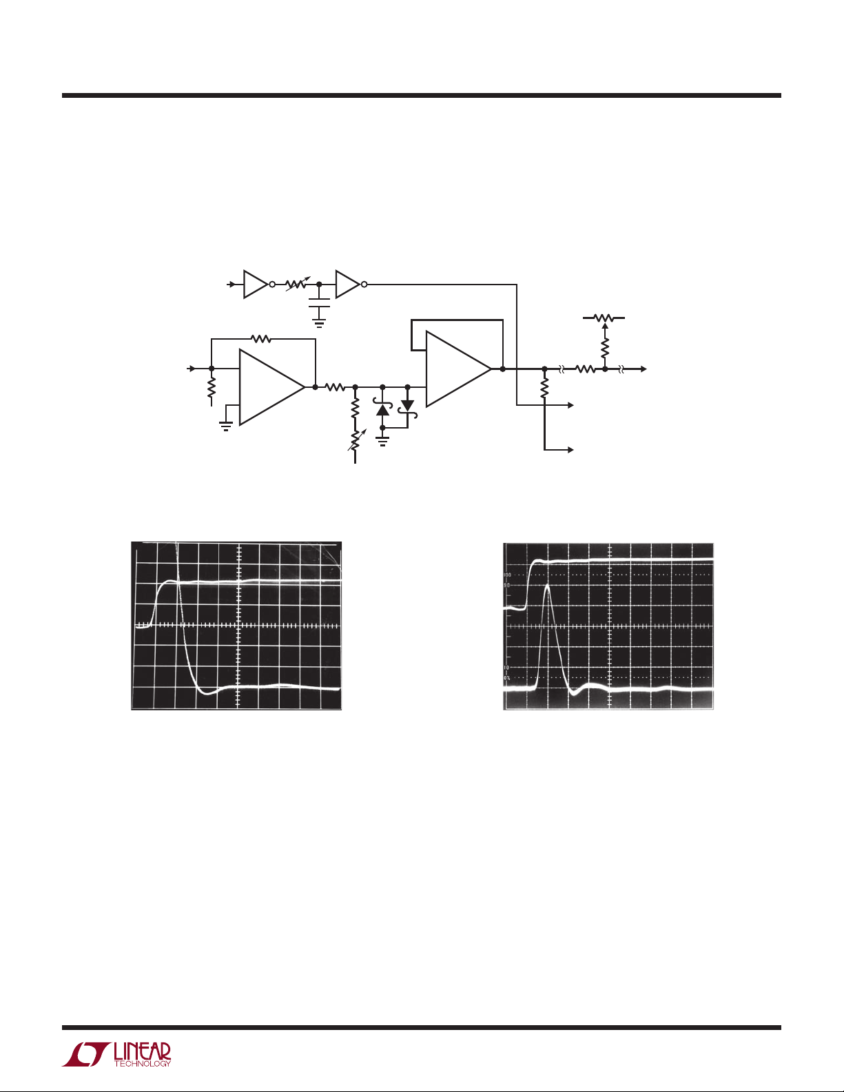
VERIFYING RESULTS–ALTERNATE METHOD
The sampling-based settling time circuit appears to be
a useful measurement solution. How can its results be
tested to ensure confidence? A good way is to make the
same measurement with an alternate method and see if
results agree. It was stated earlier that classical sampling
10
oscilloscopes were inherently immune to overdrive
. If
this is so, why not utilize this feature and attempt settling
time measurement directly at the clamped settle node?
Figure 8 does this. Under these conditions, the sampling
11
scope
is heavily overdriven, but is ostensibly immune to
the insult. Figure 9 puts the sampling oscilloscope to the
test. Trace A is the time corrected input pulse and Trace B
the settle signal. Despite a brutal overdrive, the ‘scope
appears to respond cleanly, giving a very plausible settle
signal presentation.
SUMMARY OF RESULTS AND MEASUREMENT LIMITS
A = 2V/DIV
B = 10mV/DIV
HORIZ = 5ns/DIV
Figure 7. Expanded Vertical and Horizontal Scales Show
9ns Amplifier Settling within 5mV (Trace B). Trace A Is
Time Corrected Input Step
Note 7. When interpreting waveform placement note that trace B appears
time skewed relative to time corrected trace A. This accounts for trace B’s
falsely apparent movement before trace A’s ascent.
AN128 F07
AN128-6
The simplest way to summarize the different method’s
results is by visual comparison. Ideally, if both approaches
represent good measurement technique and are properly
constructed, results should be identical. If this is the case,
the data produced by the two methods has a high probability
of being valid. Examination of Figures 9 and 10 shows
Note 8. In this and all following photos, settling time is measured from
the onset of the time-corrected input pulse. Additionally, settling signal
amplitude is calibrated with respect to the amplifier, not the settle node.
This eliminates ambiguity due to the settle node’s resistance ratio.
Note 9. This section mentions amplifier frequency compensation within
the context of sampling-based settling time measurement. As such, it
is necessarily brief. Considerably more detail is available in Appendix B,
“Practical Considerations for Amplifier Compensation.”
Note 10. See Appendix C, “Evaluating Oscilloscope Overdrive
Performance” for in-depth discussion.
Note 11. Tektronix type 661 with 4S1 vertical and 5T3 timing plug-ins.
an128f
Page 7
Application Note 128
nearly identical settling times and highly similar settling
waveform signatures. This kind of agreement provides a
high degree of credibility to the measured results.
Close observation of settling time circuit operation
indicates a noise floor/feedthrough imposed amplitude
FROM CURRENT
SWITCH DRIVER
FROM DIODE
BRIDGE CURRENT
SWITCH
ADJUST FOR 6.65ns DELAY COMPENSATION
1k
–5
SEE APPENDIX A
B
499
–
LT1818
+
1k
5pF
1k
1.5k
SETTLE
NODE
ZERO
B
1k
HSMS-2860
2s
+5
resolution limit of 2mV. The time resolution limit is about
2 nanoseconds to 5mV settling. For details, see the section
“Measurement Limits and Uncertainties”, in Appendix A,
“Measuring and Compensating Settling Circuit Delay and
Trimming Procedures.”
Y OFFSET
1k
+5 –5
–
LT1818
+
A1
50
10k
47
TO TEKTRONIX 661/4S1/5T3
SAMPLING SCOPE CHANNEL A
100X PROBE (TEKTRONIX P-6057)
VIA Z
0
TO CHANNEL B VIA 50 CABLE
DELAY MATCHED TO CHANNEL A
PROBE
Z
0
TO SAMPLE GATE
AN128 F08
Figure 8. Settling Time Test Circuit Modifications Using Classical Tektronix 661/4S1/5T3 1GHz Sampling Oscilloscope. Sampling
‘Scope’s Inherent Overload Immunity Permits Large Off-Screen Excursions without Degrading Measurement Fidelity
A = 2V/DIV
B = 10mV/DIV
HORIZ = 5ns/DIV
AN128 F09
Figure 9. Settling Time Measurement with Classical Sampling
‘Scope. Oscilloscope’s Overload Immunity Allows Accurate
Measurement Despite Extreme Overdrive. 9ns Settling Time and
Waveform Profile Are Consistent with Figure 7
REFERENCES
1. Williams, Jim, “1ppm Settling Time Measurement for
a Monolithic 18-Bit DAC,” Linear Technology Corporation, Application Note 120, February 2010.
2. Williams, Jim, “30 Nanosecond Settling Time
Measurement for a Precision Wideband Amplifier,”
Linear Technology Corporation, Application Note 79,
September 1999.
A = 2V/DIV
B = 10mV/DIV
HORIZ = 5ns/DIV
AN128 F10
Figure 10. Settling Time Measurement Using Figure 5’s Circuit.
T
= 9ns. Results Correlate with Figure 9
SETTLE
3. Williams, Jim, “Component and Measurement Advances Ensure 16-Bit DAC Settling Time,” Linear
Technology Corporation, Application Note 74, July
1998.
4. Williams, Jim, “Measuring 16-Bit Settling Times: The
Art of Timely Accuracy,” EDN, November 19, 1998.
5. Williams, Jim, “Methods for Measuring Op Amp Settling Time,” Linear Technology Corporation, Application
Note 10, July 1985.
an128f
AN128-7
Page 8

Application Note 128
6. LT1818 Data Sheet, Linear Technology Corporation.
7. AD835 Data Sheet, Analog Devices, Inc.
8. Elbert, Mark, and Gilbert, Barrie, “Using the AD834 in
DC to 500MHz Applications: RMS-to-DC Conversion,
Voltage-Controlled Amplifiers, and Video Switches”,
p. 6-47. “The AD834 as a Video Switch”, “Applications
Reference Manual”, Analog Devices, Inc., 1993.
9. Kayabasi, Cezmi, “Settling Time Measurement Techniques Achieving High Precision at High Speeds,” MS
Thesis, Worcester Polytechnic Institute, 2005.
10. Demerow, R., “Settling Time of Operational Amplifiers,”
Analog Dialogue, Volume 4-1, Analog Devices, Inc.,
1970.
11. Pease, R.A., “The Subtleties of Settling Time,” The
New Lightning Empiricist, Teledyne Philbrick, June
1971.
12. Harvey, Barry, “Take the Guesswork Out of Settling
Time Measurements,” EDN, September 19, 1985.
13. Williams, Jim, “Settling Time Measurement Demands
Precise Test Circuitry,” EDN, November 15, 1984.
Technology Corporation, Application Note 122, January
2009, p.14-19.
22. Korn, G.A. and Korn, T.M., “Electronic Analog and
Hybrid Computers,” “Diode Switches,” p. 223-226.
McGraw-Hill, 1964.
23. Carlson, R., “A Versatile New DC-500MHz Oscilloscope
with High Sensitivity and Dual Channel Display,”
Hewlett-Packard Journal, Hewlett-Packard Company,
January 1960.
24. Tektronix, Inc. “Sampling Notes,” Tektronix, Inc.,
1964.
25. Tektronix, Inc. “Type 1S1 Sampling Plug-In Operating
and Service Manual,” Tektronix, Inc. 1965.
26. Mulvey, J. “Sampling Oscilloscope Circuits,” Tektronix,
Inc., Concept Series, 1970.
27. Addis, John, “Sampling Oscilloscopes,” Private Communication, February 1991.
28. Williams, Jim, “Bridge Circuits–Marrying Gain and
Balance,” Linear Technology Corporation, Application
Note 43, June 1990.
14. Schoenwetter, H.R., “High Accuracy Settling Time
Measurements,” IEEE Transactions on Instrumentation
and Measurement, Vol. IM-32. No.1, March 1983.
15. Sheingold, D.H., “DAC Settling Time Measurement,”
Analog-Digital Conversion Handbook, pg. 312-317.
Prentice Hall, 1986.
16. Orwiler, Bob, “Oscilloscope Vertical Amplifiers,” Tektronix, Inc., Concept Series, 1969.
17. Addis, John, “Fast Vertical Amplifiers and Good Engineering,” Analog Circuit Design; Art, Science and
Personalities, Butterworths, 1991.
18. Travis, W., “Settling Time Measurement Using Delayed
Switch,” Private Communication, 1984.
19. Hewlett-Packard, “Schottky Diodes for High Volume,
Low Cost Applications,” Application Note 942, HewlettPackard Company, 1973.
20. Williams, Jim, “Signal Sources, Conditioners and
Power Circuitry,” Linear Technology Corporation,
Application Note 98, November 2004, p. 26-27.
21. Williams, Jim and Beebe, David, “Diode Turn-On
Induced Failures in Switching Regulators”, Linear
29. Tektronix, Inc., “Type 661 Sampling Oscilloscope Operating and Service Manual,” Tektronix, Inc., 1963.
30. Tektronix, Inc., “Type 4S1 Sampling Plug-In Operating
and Service Manual,” Tektronix, Inc., 1963.
31. Tektronix, Inc., “Type 5T3 Timing Unit Operating and
Service Manual,” Tektronix, Inc., 1965.
32. Morrison, Ralph, “Grounding and Shielding Techniques
in Instrumentation,” 2nd Edition, Wiley Interscience,
1977.
33. Ott, Henry W., “Noise Reduction Techniques in Electronic Systems,” Wiley Interscience, 1976.
34. Williams, Jim, “High Speed Amplifier Techniques,”
Linear Technology Corporation, Application Note 47,
1991.
35. Weber, Joe, “Oscilloscope Probe Circuits,” Tektronix,
Inc., Concept Series, 1969.
36. Ott, Henry, “Electromagnetic Compatibility Engineering,” Wiley and Sons, 2009.
37. Bogatin, Eric, “Signal and Power Integrity–Simplified,”
2nd Edition, Prentice Hall, 2009.
an128f
AN128-8
Page 9

APPENDIX A
Measuring and Compensating Settling Circuit Delay
and Trimming Procedures
The settling time circuit requires trimming to achieve
quoted performance. The trims fall into four loosely
defined categories including current switch bridge drive
pulse shaping, circuit delays, sample gate pulse purity and
1
sample gate feedthrough/DC adjustments
.
Application Note 128
A = 0.5V/DIV
Bridge Drive Trims
The current switch bridge drive is trimmed first. Disconnect all 5 bridge drive related trims and apply a 5V, 1MHz,
10 to 15 nanosecond wide pulse at the circuit input. The
paralleled “C” inverter output viewed at the 43Ω back
termination’s undriven end should resemble Figure A1.
Waveform edge times are fast but poorly controlled parasitic excursions risk corrupting the measurement noise
floor and must be eliminated. Reconnect all 5 trims and
adjust them according to their titles for Figure A2’s much
improved presentation. There is some interaction between
the adjustments but it is limited and favorable results are
easily attained. Figure A2’s edge times are slightly slower
than Figure A1’s, but still pass through the 1N5712 clamp
level in <1 nanosecond.
Delay Determination and Compensation
Circuit delay related trims come next. Before making these
measurements and adjustments, probe/oscilloscope channel-to-channel time skewing must be corrected. Figure A3
shows 40 picosecond time skew error with both channel
probes connected to a 100 picosecond rise time pulse
2
source
. The error is corrected in Figure A4 by utilizing
the oscilloscopes vertical amplifier variable delay feature
(Tektronix 7A29, option 04, installed in a Tektronix 7104
mainframe). This correction permits high accuracy delay
3
measurements to be made
Note 1. The trims require considerable care in instrumentation selection
as well as thoughtful wideband probing and oscilloscope measurement
technique. See Appendixes D through H for tutorial guidance before
proceeding.
Note 2. See Appendix H, “Verifying Rise Time and Delay Measurement
Integrity” for fast pulse source recommendations.
Note 3. This assumes the oscilloscope time base has been verified for
accuracy. For recommendations, see Appendix H, “Verifying Rise Time and
Delay Measurement Integrity”.
.
HORIZ = 2ns/DIV
Figure A1. Untrimmed Current Switch Driver Response at 43Ω
Back Termination Viewed in 1GHz, Real Time Bandwidth. Edge
Times Are Fast, But Poorly Controlled. Undamped Waveform
Artifacts Risk Corrupting Signal Path Noise Floor Via Radiation
and Ground Current Disruption Induced Errors
A = 0.5V/DIV
HORIZ = 2ns/DIV
Figure A2. Trimmed Current Switch Driver Output at 43Ω
Back Termination Passes Through 0.6V Diode Clamp
Potential in <1 Nanosecond. AC Trims Promote Clean,
Well Controlled Waveform
A = 0.1V/DIV
B = 0.1V/DIV
HORIZ = 200ps/DIV
Figure A3. Probe-Oscilloscope Channel-to-Channel Timing Skew
Measures 40 Picoseconds
AN128 FA01
AN128 FA02
AN128 FA03
an128f
AN128-9
Page 10

Application Note 128
A = 0.1V/DIV
B = 0.1V/DIV
HORIZ = 200ps/DIV
Figure A4. Corrected Probe/Channel/Skew Shows Nearly
Identical Time and Amplitude Response
AN128 FA04
The settling time circuit utilizes an adjustable delay network
to time correct the input pulse for delays in the signalprocessing path. Typically, these delays introduce errors
approaching 10 nanoseconds, so an accurate correction
is required. Setting the delay trim involves observing
the network’s input-output delay and adjusting for the
appropriate time interval. Determining the “appropriate”
time interval is somewhat more complex.
Referring to Figure 5, it is apparent that three delay measurements are of interest. The current switch driver to
amplifier-under-test negative input, the amplifier-under-test
output to circuit output and the sample gate multiplier
delay. Figure A5 indicates 250 picoseconds delay from
the current switch driver to the amplifier-under-test input. Figure A6 reveals 8.4 nanoseconds delay from the
amplifier-under-test output to circuit output and Figure
A7 shows sample gate multiplier delay of 2 nanoseconds.
The measurements indicate a current switch driver-to-circuit output delay of 8.65 nanoseconds; the correction is
implemented by adjusting the 1k trim in the “Signal Path
Delay Compensation” network for that amount. Similarly,
when the sampling ‘scope is used, the relevant delays are
Figure A5 plus A6 minus Figure A7, a total of 6.65 nanoseconds. This factor is adjusted into the signal path delay
compensation network when the sampling ‘scope-based
measurement is taken.
A = 5V/DIV
B = 20mA/DIV
HORIZ = 500ps/DIV
Figure A5. Current Switch Driver (Trace A) to Amplifier-UnderTest Negative Input (Trace B) Delay Is 250 Picoseconds
A = 2V/DIV
B = 0.2V/DIV
HORIZ = 2ns/DIV
Figure A6. Amplifier-Under-Test (Trace A) to Circuit Output
(Trace B) Delay Measures 8.4 Nanoseconds. Multiplier X
Input Held at 1V DC for This Test
A = 0.1V/DIV
B = 0.1V/DIV
HORIZ = 2ns/DIV
Figure A7. Multiplier Delay with X Input Held at 1V DC
Measures 2ns
AN128 FA05
AN128 FA06
AN128 FA07
The “Sample Gate Pulse Generator Path Delay Compensation” trim is less critical. The sole requirement is that
it overlap the sample gate pulse generator’s delay. Setting the 1k potentiometer in the “A” inverter chain to 15
nanoseconds satisfies this criteria, completing the delay
related trims.
AN128-10
Sample Gate Pulse Purity Adjustment
The Q1 sample gate pulse edge shaping stage is adjusted
for an optimized front corner, minimum rising edge time,
pulse top smoothing and 1V amplitude with the indicated
trims. The mildly interactive adjustments converge to
an128f
Page 11

A = 0.2V/DIV
Application Note 128
A = 1V/DIV
B = 10mV/DIV
HORIZ = 5ns/DIV
Figure A8. Sample Gate Pulse Characteristics, Controlled
by Edge Shaping, Circuit Configuration and Transistor
Choice, Are Kept Within Multiplier’s 250MHz (T
Bandwidth. Accurate, Low Feedthrough, Y Input Signal Path
Switching Results
AN128 FA08
RISE
= 1.4ns)
Figure A8’s display, taken at the sample gate multiplier’s X
input. The pulse’s 2 nanosecond rise time promotes rapid
sample gate acquisition but remains within the multipliers
250MHz (t
= 1.4ns) bandwidth, assuring freedom from
RISE
out-of-band parasitic responses. The clean, 1V amplitude pulse top provides calibrated, consistent multiplier
output devoid of aberrations which would masquerade
as settling signal artifacts. Pulse fall time is irrelevant; it
is not germaine to the measurement and its clean falling
transition assures controlled multiplier turn-off, precluding
off-screen excursions.
Sample Gate Path Optimization
The sample gate path adjustments are the final trims.
First, put in 5V DC to the pulse generator input to lock the
amplifier-under-test into its –2.5V output state. Adjust the
“settle node zero” trim for zero volts within 1mV at A1’s
output. Next, restore the pulsed circuit input, disconnect
the settle node from A1 and ground A1’s input with a 750Ω
resistor. Figure A9 is typical of the resultant untrimmed
response. Ideally, the circuit output (trace B) should be
static during sample gate (trace A) switching. The photo
reveals errors; correction requires trimming DC offset
and dynamic feedthrough related residue. The DC errors
are eliminated by adjusting the “X” and “Y” offset trims
for a continuous trace B baseline regardless of trace A’s
sample gate pulse state. Additionally, set the output offset
adjustment for minimum multiplier baseline offset voltage. Sample gate gain is set to unity by shutting off the
input pulse generator, applying 5V DC to C2’s “+” input
HORIZ = 10ns/DIV
Figure A9. Settling Time Circuit’s Output (Trace B) with
Unadjusted Sample Gate Feedthrough and DC Offset.
A1’s Input Grounded for This Test. Excessive Switch Drive
Feedthrough and Baseline Offset Are Present. Trace A Is
Sample Gate Pulse
AN128 FA09
and forcing 1.00V DC at the previously inserted 750
resistor. Under these conditions, adjust “scale factor” for
1.00V DC output. After completing this step, remove the
DC bias voltages and the 750 resistor, reconnect the
settle node and restore the pulsed input.
Feedthrough compensation is accomplished via
feedthrough “time phase” and “amplitude” trims. These
adjustments set timing and amplitude of the feedthrough
correction applied at the multiplier “Z” input. Optimal
adjustment results in Figure A10’s presentation. This
photograph shows the DC and feedthrough trims dramatic
4
effect on Figure A9’s pre-trim errors
A = 1V/DIV
B = 10mV/DIV
HORIZ = 10ns/DIV
Figure A10. Settling Time Circuit’s Output (Trace B) with Sample
Gate Trimmed. As in Figure A9, A1’s Input Is Grounded for
This Test. Switch Drive Feedthrough and Baseline Offset Are
Minimized. Trace A Is Sample Gate Pulse. Measurement Defines
Circuit’s 2mV Minimum Amplitude Resolution Limit
Note 4. The writer is not much for Hollywood’s offerings, but does find
drama in feedthrough trims.
.
AN128 FA10
an128f
AN128-11
Page 12

Application Note 128
Measurement Limits and Uncertainties
Figure A10’s post trim response includes a flat baseline
and greatly attenuated feedthrough. The measurement
defines the circuit’s minimum amplitude resolution at
2mV. In another test, A1’s input is disconnected from the
settle node and biased at 20mV DC via a 750Ω resistor
to simulate an infinitely fast settling amplifier. Figure A11
shows circuit output (trace B) settling within 5mV in 2
nanoseconds, arriving inside the 2mV baseline noise limit
in 3.6 nanoseconds. This data, taken with sample gate
conduction beginning immediately after the time corrected
input (trace A) rises, defines the circuit’s minimum time
resolution limit. Uncertainties in the quoted time and
amplitude resolution limits are primarily due to delay
compensation limitations, noise and residual feedthrough.
Considering likely delay and measurement errors, a time
uncertainty of ±500 picoseconds and a 2mV resolution limit
APPENDIX B
is probably realistic. Noise averaging would not improve
the amplitude resolution limit because it is imposed by
feedthrough residue, a coherent term.
A = 2V/DIV
B = 10mV/DIV
HORIZ = 2ns/DIV
Figure A11. Circuit Response with 20mV DC Forced at A1’s
Input. Output (Trace B) Is within 5mV in 2ns, Arriving Inside
2mV Baseline Noise in 3.6ns. Measurement Defines Circuits
Minimum Time Resolution Limit. Trace A Is Time Corrected
Input Pulse
AN128 FA11
Practical Considerations for Amplifier Compensation
There are a number of practical considerations in compensating the amplifier to get fastest settling time. Our
study begins by revisiting text Figure 1 (repeated here as
Figure B1). Settling time components include delay, slew
and ring times. Delay is due to propagation time through
the amplifier and is a relatively small term. Slew time is
set by the amplifier’s maximum speed. Ring time defines
the region where the amplifier recovers from slewing and
ceases movement within some defined error band. Once
an amplifier has been chosen, only ring time is readily
adjustable. Because slew time is usually the dominant
lag, it is tempting to select the fastest slewing amplifier
SETTLING TIME
INPUT
RING TIME
ALLOWABLE
OUTPUT
ERROR
OUTPUT
Figure B1. Settling Time Components Include Delay, Slew and
Ring Times. For Given Components, Only Ring Time Is Readily
Adjustable
SLEW
TIME
DELAY TIME
BAND
AN128 FB01
available to obtain best settling. Unfortunately, fast slewing
amplifiers usually have extended ring times, negating their
brute force speed advantage. The penalty for raw speed is,
invariably, prolonged ringing, which can only be damped
with large compensation capacitors. Such compensation
works, but results in protracted settling times. The key
to good settling times is to choose an amplifier with the
right balance of slew rate and recovery characteristics
and compensate it properly. This is harder than it sounds
because amplifier settling time cannot be predicted or
extrapolated from any combination of data sheet specifications. It must be measured in the intended configuration.
A number of terms combine to influence settling time.
They include amplifier slew rate and AC dynamics, layout
capacitance, source resistance and capacitance, and the
compensation capacitor. These terms interact in a complex
1
manner, making predictions hazardous
. If the parasitics
are eliminated and replaced with a pure resistive source,
amplifier settling time is still not readily predictable. The
parasitic impedance terms just make a difficult problem
more messy. The only real handle available to deal with
all this is the feedback compensation capacitor, C
. CF’s
F
purpose is to roll off amplifier gain at the frequency that
permits best dynamic response.
Note 1. Spice aficionados take notice.
an128f
AN128-12
Page 13

Best settling results when the compensation capacitor
is selected to functionally compensate for all the above
terms. Figure B2 shows results for an optimally selected
feedback capacitor. Trace A is the time-corrected input
pulse and trace B the amplifier’s settle signal. The amplifier comes cleanly out of slew (sample gate opens just
after the second vertical division) and settles to 5mV in
9 nanoseconds. Waveform signature is tight and nearly
critically damped.
A = 2V/DIV
B = 10mV/DIV
Application Note 128
A = 2V/DIV
B = 20mV/DIV
HORIZ = 5ns/DIV
Figure B3. Overdamped Response Ensures Freedom from
Ringing, Even with Component Variations in Production. Penalty
Is Increased Settling Time. Note 2X Vertical Scale Change vs.
Figure B2. T
Figure
A = 2V/DIV
= 22ns. Trace Assignments Same as Previous
SETTLE
AN128 FB03
HORIZ = 5ns/DIV
Figure B2. Optimized Compensation Capacitor Permits Tight
Waveform Signature, Nearly Critically Damped Response and
Fastest Settling Time. T
Input Step, Trace B, the Settle Signal
= 9ns. Trace A Is Time Corrected
SETTLE
AN128 FB02
In Figure B3, the feedback capacitor is too large. Settling is smooth, although overdamped; a 13 nanosecond
penalty results in 22 nanosecond settling. Figure B4 has
no feedback capacitor, causing severely underdamped
response with resultant excessive ring time excursions.
Settling time goes out to 33 nanoseconds. B5 improves
on B4 by restoring the feedback capacitor, but the value is
too small, resulting in an underdamped response requiring 27 nanoseconds to settle. Note that Figures B3 to B5
require vertical scale reduction to capture non-optimal
response.
When feedback capacitors are individually trimmed for
optimal response, the source, stray, amplifier and compensation capacitor tolerances are irrelevant. If individual
trimming is not used, these tolerances must be considered
to determine the feedback capacitor’s production value.
Ring time is affected by stray and source capacitance and
output loading, as well as the feedback capacitor’s value.
The relationship is nonlinear, although some guidelines are
B = 50mV/DIV
HORIZ = 5ns/DIV
Figure B4. Severely Underdamped Response Due to No
Feedback Capacitor. Note 5X Vertical Scale Change vs Figure B2.
T
= 33ns. Trace Assignments as in Figure B2
SETTLE
A = 2V/DIV
B = 50mV/DIV
HORIZ = 5ns/DIV
Figure B5. Underdamped Response Results from Undersized
Capacitor. Component Tolerance Budgeting Will Prevent
This Behavior. Note 5x Vertical Scale Change vs. Figure B2.
T
= 27ns. Trace Assignments as in Figure B2
SETTLE
AN128 FB04
AN128 FB05
an128f
AN128-13
Page 14

Application Note 128
possible. The stray and source terms can vary by ±10%
2
and the feedback capacitor is typically a ±5% component
.
Additionally, amplifier slew rate has a significant tolerance,
which is stated on the data sheet. To obtain a production
feedback capacitor value, determine the optimum value
by individual trimming with the production board layout
(board layout parasitic capacitance counts too!). Then,
factor in the worst-case percentage values for stray
and source impedance terms, slew rate and feedback
APPENDIX C
Evaluating Oscilloscope Overdrive Performance
The sampling based settling time circuit is heavily oriented
towards preventing overdrive to the monitoring oscilloscope. This is done to avoid overdriving the oscilloscope.
Oscilloscope recovery from overdrive is a grey area and
almost never specified. How long must one wait after an
overdrive before the display can be taken seriously? The
answer to this question is quite complex. Factors involved
include the degree of overdrive, its duty cycle, its magnitude in time and amplitude and other considerations.
Oscilloscope response to overdrive varies widely between
types and markedly different behavior can be observed
in any individual instrument. For example, the recovery
time for a 100x overload at 0.005V/DIV may be very different than at 0.1V/DIV. The recovery characteristic may
also vary with waveform shape, DC content and repetition
rate. With so many variables, it is clear that measurements
involving oscilloscope overdrive must be approached with
caution.
Why do most oscilloscopes have so much trouble recovering from overdrive? The answer to this question requires
some study of the three basic oscilloscope types’ vertical
path. The types include analog (Figure C1A), digital (Figure
C1B) and classical sampling (Figure C1C) oscilloscopes.
Analog and digital ‘scopes are susceptible to overdrive.
The classical sampling ‘scope is the only architecture that
is inherently immune to overdrive.
An analog oscilloscope (Figure C1A) is a real time, continu-
1
ous linear system
. The input is applied to an attenuator,
which is unloaded by a wideband buffer. The vertical preamp
provides gain, and drives the trigger pick-off, delay line and
the vertical output amplifier. The attenuator and delay line
capacitor tolerance. Add this information to the trimmed
capacitors measured value to obtain the production value.
This budgeting is perhaps unduly pessimistic (RMS error
summing may be a defensible compromise), but will keep
3
you out of trouble
Note 2. This assumes a resistive source. If the source has substantial
parasitic capacitance (photodiode, DAC, etc.), this number can easily
enlarge to ±50%.
Note 3. The potential problems with RMS error summing become clear
when sitting in an airliner that is landing in a snowstorm.
.
are passive elements and require little comment although
they can display reactive behavior at speed and resolution
extremes. The buffer, preamp and vertical output amplifier
are complex linear gain blocks, each with dynamic operating
range restrictions. Additionally, the operating point of each
block may be set by inherent circuit balance, low frequency
stabilization paths or both. When the input is overdriven,
one or more of these stages may saturate, forcing internal
nodes and components to abnormal operating points and
temperatures. When the overload ceases, full recovery
of the electronic and thermal time constants may require
2
surprising lengths of time
.
The digital sampling oscilloscope (Figure C1B) eliminates
the vertical output amplifier, but has an attenuator buffer and
amplifiers ahead of the A/D converter. Because of this, it is
similarly susceptible to overdrive recovery problems.
The classical sampling oscilloscope is unique. Its nature
of operation makes it inherently immune to overload.
Figure C1C shows why. The sampling occurs before any
gain is taken in the system. Unlike Figure C1B’s digitally
sampled ‘scope, the input is fully passive to the sampling
point. Additionally, the output is fed back to the sampling
bridge, maintaining its operating point over a very wide
range of inputs. The dynamic swing available to maintain
the bridge output is large and easily accommodates a wide
range of oscilloscope inputs. Because of all this, the amplifiers in this instrument do not see overload, even at 1000x
overdrives, and there is no recovery problem. Additional
immunity derives from the instrument’s relatively slow
Note 1. Ergo, the Real Thing. Hopelessly bigoted residents of this locale
mourn the passing of the analog ‘scope era and frantically hoard every
instrument they can find.
Note 2. Some discussion of input overdrive effects in analog oscilloscope
circuitry is found in Reference 17.
an128f
AN128-14
Page 15

INPUT
ATTENUATOR ATTENUATOR
BUFFER
+
V
Application Note 128
A
ANALOG
OSCILLOSCOPE
VERTICAL
CHANNEL
B
DIGITAL
SAMPLING
OSCILLOSCOPE
VERTICAL
CHANNEL
INPUT
ATTENUATOR
–
V
ATTENUATOR
BUFFER
+
V
–
V
VERTICAL
PREAMP
VERTICAL
PREAMP
+
V
V
TRIGGER
CIRCUITRY
DELAY LINE
TRIGGER
CIRCUITRY
A/D DRIVER
AMP
–
A/D CONTROL
A/D
PULSE STRETCHER—
MEMORY SWITCH
DRIVER
VERTICAL
OUTPUT
SAMPLE
COMMAND
TO HORIZONTAL/
SWEEP SECTION
TO CRT
TIMING
GENERATOR
MEMORY
MICROPROCESSOR
TO CRT
MEMORY
INPUT
C
CLASSICAL
SAMPLING
OSCILLOSCOPE
VERTICAL
CHANNEL
DELAY LINE
TRIGGER
CIRCUITRY
+
V–V
TO HORIZONTAL CIRCUITS
AC
AMPLIFIER
DC OFFSET
GENERATOR
FEEDBACK
AMPLIFIER
Figure C1. Simplified Vertical Channel Diagrams for Different Type Oscilloscopes. Only the Classical Sampling ‘Scope (C)
Has Inherent Overdrive Immunity. Offset Generator Allows Viewing Small Signals Riding On Large Excursions
sample rate—even if the amplifiers were overloaded, they
would have plenty of time to recover between samples
The designers of classical sampling ‘scopes capitalized
on the overdrive immunity by including variable DC offset
generators to bias the feedback loop (see Figure C1C, lower
right). This permits the user to offset a large input, so small
amplitude activity on top of the signal can be accurately
observed. This is ideal for, among other things, settling
3
.
time measurements. Unfortunately, classical sampling
oscilloscopes are no longer manufactured, so if you have
4
one, take care of it
Note 3. Additional information and detailed treatment of classical sampling
oscilloscope operation appears in References 23-26 and 29-31.
Note 4. Modern variants of the classical architecture (e.g., Tektronix
11801B) may provide similar capability, although we have not tried them.
!
TO CRT
VERTICAL
AN128 FC01
an128f
AN128-15
Page 16

Application Note 128
Although analog and digital oscilloscopes are susceptible
to overdrive, many types can tolerate some degree of this
abuse. The early portion of this appendix stressed that
measurements involving oscilloscope overdrive must
be approached with caution. Nevertheless, a simple test
can indicate when the oscilloscope is being deleteriously
affected by overdrive.
The waveform to be expanded is placed on the screen at
a vertical sensitivity that eliminates all off-screen activity.
Figure C2 shows the display. The lower right hand portion
A = 1V/DIV
100ns/DIV
Figure C2
AN128 FC02
is to be expanded. Increasing the vertical sensitivity by a
factor of two (Figure C3) drives the waveform off-screen,
but the remaining display appears reasonable. Amplitude
has doubled and waveshape is consistent with the original
display. Looking carefully, it is possible to see small amplitude information presented as a dip in the waveform at
about the third vertical division. Some small disturbances
are also visible. This observed expansion of the original
waveform is believable. In Figure C4, gain has been further
increased, and all the features of Figure C3 are amplified
A = 0.1V/DIV
100ns/DIV
Figure C5
AN128 FC05
A = 0.5V/DIV
A = 0.2V/DIV
A = 0.1V/DIV
100ns/DIV
Figure C3
100ns/DIV
Figure C4
AN128 FC03
AN128 FC04
100ns/DIV
Figure C6
A = 0.1V/DIV
100ns/DIV
Figure C7
Figure C2 to C7. The Overdrive Limit Is Determined by Progressively Increasing
Oscilloscope Gain and Watching for Waveform Aberrations
AN128 FC06
AN128 FC07
an128f
AN128-16
Page 17

Application Note 128
accordingly. The basic waveshape appears clearer and the
dip and small disturbances are also easier to see. No new
waveform characteristics are observed. Figure C5 brings
some unpleasant surprises. This increase in gain causes
definite distortion. The initial negative-going peak, although
larger, has a different shape. Its bottom appears less broad
than in Figure C4. Additionally, the peak’s positive recovery
is shaped slightly differently. A new rippling disturbance
is visible in the center of the screen. This kind of change
indicates that the oscilloscope is having trouble. A further
test can confirm that this waveform is being influenced
by overloading. In Figure C6 the gain remains the same
APPENDIX D
ABOUT Z
PROBES
0
When to Roll Your Own and When to Pay the Money
(e.g. low impedance) probes provide the most faithful
Z
0
high speed probing mechanism available for low source
impedances. Their sub-picofarad input capacitance and
near ideal transmission characteristic make them the
first choice for high bandwidth oscilloscope measurement. Their deceptively simple operation invites “do-ityourself” construction but numerous subtleties mandate
difficulty for prospective constructors. Arcane parasitic
effects introduce errors as speed increases beyond about
100MHz (t
= 3.5ns). The selection and integration
RISE
of probe materials and the probes physical incarnation
require extreme care to obtain high fidelity at high speed.
Additionally, the probe must include some form of adjustment to compensate small, residual parasitics. Finally, true
coaxiality must be maintained when fixturing the probe
at the measurement point, implying a high grade, readily
disconnectable, coaxial connection capability.
Figure D1 shows that a Z
probe is basically a voltage di-
0
vided input 50 transmission line. If R1 equals 450, 10x
attenuation and 500 input resistance result. R1 of 4950
causes a 100x attenuation with 5k input resistance. The 50
line theoretically constitutes a distortionless transmission
environment. The apparent simplicity seemingly permits
“do-it-yourself” construction but this section’s remaining
figures demonstrate a need for caution.
Figure D2 establishes a fidelity reference by measuring a
clean 700ps rise time pulse using a 50 line terminated
but the vertical position knob has been used to reposi-
5
tion the display at the screen’s bottom
. This shifts the
oscilloscope’s DC operating point which, under normal
circumstances, should not affect the displayed waveform.
Instead, a marked shift in waveform amplitude and outline
occurs. Repositioning the waveform to the screen’s top
produces a differently distorted waveform (Figure C7).
It is obvious that for this particular waveform, accurate
results cannot be obtained at this gain.
Note 5. Knobs (derived from Middle English, “knobbe”, akin to Middle
Low German, “knubbe”), cylindrically shaped, finger rotatable panel
controls for controlling instrument functions, were utilized by the ancients.
R1
450
Figure D1. Conceptual 500Ω, “Z0”, 10x Oscilloscope Probe. If
R1 = 4950Ω, 5k Input Resistance with 100x Signal Attenuation
Results. Terminated Into 50Ω, Probe Theoretically Constitutes
Distortionless Transmission Line. “Do-It-Yourself” Probes Suffer
Uncompensated Parasitics, Causing Unfaithful Response Above
≈ 100MHz (t
1V/DIV
Figure D2. 700ps Rise Time Pulse Observed via 50Ω Line
and 10x Coaxial Attenuator Has Good Pulse Edge Fidelity with
Controlled Post-Transition Events
RISE
= 3.5ns)
50 COAXIAL CABLE
500ps/DIV
OUTPUT TO 50
OSCILLOSCOPE
AN128 FD01
AN128 FD02
via a 10x coaxial attenuator—no probe is employed. The
waveform is singularly clean and crisp with minimal edge
and post-transition aberrations. Figure D3 depicts the
same pulse with a commercially produced 10x Z
probe
0
in use. The probe is faithful and there is barely discernible
error in the presentation. Photos D4 and D5, taken with
an128f
AN128-17
Page 18

Application Note 128
1V/DIV
500ps/DIV
Figure D3. Figure D2’s Pulse Viewed with Tektronix 10x, Z0
500Ω Probe (P-6056) Introduces Barely Discernible Error
1V/DIV
500ps/DIV
Figure D4. “Do-It-Yourself” Z0 Probe #1 Introduces Pulse
Corner Rounding, Likely Due to Resistor/Cable Parasitic Terms
or Incomplete Coaxiality. “Do-It-Yourself” Z0 Probes Typically
Manifest This Type of Error at Rise Times ≤2ns
AN128 FD03
AN128 FD04
1V/DIV
500ps/DIV
Figure D5. “Do-It-Yourself” Z0 Probe #2 Has Overshoot, Again
Likely Due to Resistor/Cable Parasitic Terms or Incomplete
Coaxiality. Lesson: At These Speeds, Don’t “Do-It-Yourself”
AN128 FD05
two separately constructed “do-it-yourself” Z0 probes,
show errors. In D4, Probe #1 introduces pulse front corner rounding; Probe #2 in D5 causes pronounced corner
peaking. In each case, some combination of resistor/cable
parasitics and incomplete coaxiality are likely responsible
for the errors. In general, “do-it-yourself” Z
these types of errors beyond about 100MHz (t
probes cause
0
3.5ns).
RISE
At higher speeds, if waveform fidelity is critical, it’s best
to pay the money. For additional terror and wisdom along
these lines, see pg. 2-4 → 2-8 of Reference 30 and Reference 35. Both are excellent, informative and, hopefully,
sobering to still undaunted do-it-yourselfers.
AN128-18
an128f
Page 19

APPENDIX E
Application Note 128
Connections, Cables, Adapters, Attenuators, Probes
and Picoseconds
Subnanosecond rise time signal paths must be considered
as a transmission line. Connections, cables, adapters,
attenuators and probes represent discontinuities in this
transmission line, deleteriously affecting its ability to
faithfully transmit desired signal. The degree of signal
corruption contributed by a given element varies with its
deviation from the transmission lines nominal impedance.
The practical result of such introduced aberrations is degradation of pulse rise time, fidelity, or both. Accordingly,
introduction of elements or connections to the signal
path should be minimized and necessary connections
and elements must be high grade components. Any form
of connector, cable, attenuator or probe must be fully
specified for high frequency use. Familiar BNC hardware
becomes lossy at rise times much faster than 350ps. SMA
components are preferred for the rise times described in
the text. Additionally, cable should be 50 “hard line”
or, at least, Teflon-based coaxial cable fully specified for
high frequency operation. Optimal connection practice
eliminates any cable by coupling the signal output directly
to the measurement input.
Mixing signal path hardware types via adapters (e.g. BNC/
SMA) should be avoided. Adapters introduce significant
parasitics, resulting in reflections, rise time degradation,
resonances and other degrading behavior. Similarly,
oscilloscope connections should be made directly to the
instrument’s 50 inputs, avoiding probes. If probes must
be used, their introduction to the signal path mandates attention to their connection mechanism and high frequency
compensation. Passive Z
types, commercially available
0
in 500 (10x) and 5k (100x) impedances, have input
1
capacitance below 1pf
. Any such probe must be carefully
frequency compensated before use or misrepresented measurement will result. Inserting the probe into the signal path
necessitates some form of signal pick-off which nominally
does not influence signal transmission. In practice, some
amount of disturbance must be tolerated and its effect on
measurement results evaluated. High quality signal pickoffs always specify insertion loss, corruption factors and
probe output scale factor.
The preceding emphasizes vigilance in designing and
maintaining a signal path. Skepticism, tempered by enlightenment, is a useful tool when constructing a signal
path and no amount of hope is as effective as preparation
and directed experimentation.
Note 1. See Appendix D, “About Z0 Probes”.
an128f
AN128-19
Page 20

Application Note 128
APPENDIX F
Breadboarding, Layout and Connection Techniques
The measurement results presented in this publication
required painstaking care in breadboarding, layout and
connection techniques. Nanosecond domain, high resolution measurement does not tolerate cavalier laboratory
attitude. The oscilloscope photographs presented, devoid
of ringing, hops, spikes and similar aberrations, are the
result of a careful breadboarding exercise. The breadboard
required considerable experimentation before obtaining a
noise/uncertainty floor worthy of the measurement.
Ohm’s Law
It is worth considering that Ohm’s law is a key to suc-
1
cessful layout
. Consider that 10mA running through 1
generates 10mV—twice the measurement limit! Now,
run that current at 1 nanosecond rise times (≈350MHz)
and the need for layout care becomes clear. A paramount
concern is disposal of circuit ground return current and
disposition of current in the ground plane. The impedance
of the ground plane between any two points is not zero,
particularly at nanosecond speeds. This is why the entry
point and flow of “dirty” ground returns must be carefully
placed within the grounding system.
losses. Every ground return and signal connection in the
entire circuit must be evaluated with these concerns in
mind. A paranoiac mindset is quite useful.
Shielding
The most obvious way to handle radiation-induced errors is shielding. Determining where shields are required
should come after considering what layout will minimize
their necessity. Often, grounding requirements conflict
with minimizing radiation effects, precluding maintaining
distance between sensitive points. Shielding is usually an
effective compromise in such situations.
A similar approach to ground path integrity should be
pursued with radiation management. Consider what points
are likely to radiate, and try to lay them out at a distance
from sensitive nodes. When in doubt about odd effects,
experiment with shield placement and note results, iterating
2
towards favorable performance
. Above all, never rely on
filtering or measurement bandwidth limiting to “get rid of”
undesired signals whose origin is not fully understood.
This is not only intellectually dishonest, but may produce
wholly invalid measurement “results,” even if they look
pretty on the oscilloscope.
A good example of the importance of grounding management involves delivering the input pulse to the breadboard.
The pulse generator’s 50 termination must be an in-line
coaxial type. This ensures that pulse generator return current circulates in a tight local loop at the terminator, and
does not mix into the signal plane. It is worth mentioning
that, because of the nanosecond speeds involved, inductive
parasitics may introduce more error than resistive terms.
This often necessitates using flat wire braid for connections to minimize parasitic inductive and skin effect-based
Connections
All signal connections to the breadboard must be coaxial.
Ground wires used with oscilloscope probes are forbidden.
A 1" ground lead used with a ‘scope probe can easily generate large amounts of observed “noise” and seemingly
inexplicable waveforms. Use coaxially mounting probe
3
tip adapters
Note 1. I do not wax pedantic here. My guilt in this matter runs deep.
Note 2. After it works, you can figure out why.
Note 3. See Reference 34 for additional nagging along these lines.
!
an128f
AN128-20
Page 21

APPENDIX G
Application Note 128
How Much Bandwidth is Enough?
Accurate wideband oscilloscope measurements require
bandwidth. A good question is just how much is needed. A
classic guideline is that “end-to-end” measurement system
rise time is equal to the root-sum-square of the system’s
individual component’s rise times. The simplest case is
two components; a signal source and an oscilloscope.
Figure G1’s plot of
signal + oscilloscope
rise time
22
versus error is illuminating. The figure plots signal-to-oscilloscope rise time ratio versus observed rise time (rise
time is bandwidth restated in the time domain, where:
2.00%
350
2.80%
)
41.00%
11.70%
5.40%
AN128 FG01
Rise Time (ns) "
50
40
30
20
10
OBSERVED RISE TIME ERROR IN PERCENT
2
0
8s 7s 6s 5s 4s 3s 2s 1s
SIGNAL-TO-OSCILLOSCOPE RISE TIME RATIO
Figure G1. Oscilloscope Rise Time Effect on Rise Time
Measurement Accuracy. Measurement Error Rises Rapidly as
Signal-to-Oscilloscope Rise Time Ratio Approaches Unity. Data,
Based on Root-Sum-Square Relationship, Does Not Include
Passive Probe, Which Does Not Follow Root-Sum-Square Law
Bandwidth (MHz)
1.37%
1.00%
The curve shows that an oscilloscope 3 to 4 times faster
than the input signal rise time is required for measurement accuracy inside about 5%. This is why trying to
measure a 1ns rise time pulse with a 350MHz oscilloscope
= 1ns) leads to erroneous conclusions. The curve
(t
RISE
indicates a monstrous 41% error. Note that this curve
does not include the effects of passive probes or cables
connecting the signal to the oscilloscope. Probes do not
necessarily follow root-sum-square law and must be
carefully chosen and applied for a given measurement.
For details, see Appendix D. Figure G2, included for reference, gives 10 cardinal points of rise time/bandwidth
equivalency between 1MHz and 5GHz.
RISE TIME BANDWIDTH
70ps 5GHz
350ps 1GHz
700ps 500MHz
1ns 350MHz
2.33ns 150MHz
3.5ns 100MHz
7ns 50MHz
35ns 10MHz
70ns 5MHz
350ns 1MHz
Figure G2. Some Cardinal Points of Rise Time/Bandwidth
Equivalency. Data Is Based on Text’s Rise Time/Bandwidth
Formula
an128f
AN128-21
Page 22

Application Note 128
APPENDIX H
Verifying Rise Time and Delay Measurement Integrity
Any measurement requires the experimenter to insure
measurement confidence. Some form of calibration check
is always in order. High speed time domain measurement
is particularly prone to error and various techniques can
promote measurement integrity.
Figure H1’s battery-powered 200MHz crystal oscillator
produces 5ns markers, useful for verifying oscilloscope
time base accuracy. A single 1.5V AA cell supplies the
LTC3400 boost regulator, which produces 5V to run the
oscillator. Oscillator output is delivered to the 50 load via
a peaked attenuation network. This provides well defined
5ns markers (Figure H2) and prevents overdriving low
level sampling oscilloscope inputs.
Once time base accuracy is confirmed it is necessary to
check rise time. The lumped signal path rise time, including
SW
LTC3400
MBR0520L
V
OUT
4.7µF
1.5V
AA CELL
4.7µF
L1 4.7µH
V
IN
attenuators, connections, cables, probes, oscilloscope and
anything else, should be included in this measurement.
Such “end-to-end” rise time checking is an effective way
to promote meaningful results. A guideline for insuring
accuracy is to have 4x faster measurement path rise time
than the rise time of interest. Thus, verifying the sample
gate multipliers 250MHz (1.4ns risetime) bandwidth
requires 1GHz (t
= 350ps) oscilloscope bandwidth.
RISE
Verifying the oscilloscope’s 350 picosecond rise time, in
turn, necessitates a 90 picosecond rise time step to ensure
the ‘scope is driven to its rise time limit. Figure H3 lists
1
some very fast edge generators for rise time checking
.
The Tektronix 284, specified at 70ps rise time, was used
to check ‘scope rise time. Figure H4 indicates 350ps rise
time, promoting measurement confidence.
Note 1. This is a fairly exotic group, but equipment of this caliber really is
necessary for rise time verification.
10pF
V
REG
1.87M*
= 5V
V
IN
200MHz
XTAL
OSCILLATOR
GND
OUT
OUTPUT
1k
(TO 50)
GND
FB
604k*
OSCILLATOR = SARONIX, SEL–24
= 1% METAL FILM RESISTOR
*
4.7µF = TAIYO YUDEN X5R EMK316BJ475ML
L1 = COILCRAFT D0160C-472
AN128 FH01
SD
Figure H1. 1.5V Powered, 200MHz Crystal Oscillator Provides 5ns Time Markers. 1.5V to 5V Switching
Regulator Powers Oscillator
an128f
AN128-22
Page 23

0.1V/DIV
Application Note 128
1ns/DIV
AN128 FH02
Figure H2. Time Mark Generator Output Terminated into 50Ω.
Peaked Waveform Is Optimal for Verifying Time Base Calibration
MANUFACTURER MODEL NUMBER RISE TIME AMPLITUDE AVAILABILITY COMMENTS
Avtech AVP2S 40ps 0V to 2V Current Production Free Running or Triggered Operation, 0MHz to 1MHz
Hewlett-Packard 213B 100ps ≈175mV Secondary Market Free Running or Triggered Operation to 100kHz
Hewlett-Packard 1105A/1108A 60ps ≈200mV Secondary Market Free Running or Triggered Operation to 100kHz
Hewlett-Packard 1105A/1106A 20ps ≈200mV Secondary Market Free Running or Triggered Operation to 100kHz
Picosecond Pulse Labs TD1110C/TD1107C 20ps ≈230mV Current Production Similar to Discontinued HP1105/1106/8A. See above.
Stanford Research
Systems
Tektronix 284 70ps ≈200mV Secondary Market 50kHz Repetition Rate. Pre-trigger 5ns, 75ns or 150ns
Tektronix 111 500ps ≈±10V Secondary Market 10kHz to 100kHz Repetition Rate. Positive or Negative
Tektronix 067-0513-00 30ps ≈400mV Secondary Market 60ns Pre-trigger Output. 100kHz Repetition Rate
Tektronix 109 250ps 0V to ±55V Secondary Market ≈600Hz Repetition Rate (High Pressure Hg Reed Relay
DG535 OPT 04A 100ps 0.5V to 2V Current Production Must be Driven with Stand-alone Pulse Generator
Before Main Output. Calibrated 100MHz and 1GHz
Sine Wave Auxiliary Outputs.
Outputs. 30ns to 250ns Pre-trigger Output. External
Trigger Input. Pulse Width Set with Charge Lines
Based). Positive or Negative Outputs. Pulse Width Set
by Charge Lines
Figure H3. Picosecond Edge Generators Suitable for Rise Time Verification. Considerations Include Speeds, Features and Availability
VERT = 50mV/DIV
HORIZ = 200ps/DIV
AN128 FH04
Figure H4. 70 Picosecond Edge Drives Oscilloscope to its 350
Picosecond Rise Time Limit, Verifing 1GHz Bandwidth
an128f
AN128-23
Page 24

Application Note 128
AN128-24
Linear Technology Corporation
1630 McCarthy Blvd., Milpitas, CA 95035-7417
(408) 432-1900 ● FAX: (408) 434-0507
●
www.linear.com
an128f
LT 0810 • PRINTED IN USA
© LINEAR TECHNOLOGY CORPORATION 2010
 Loading...