

Page 1
Application Note 126
October 2010
2-Wire Virtual Remote Sensing for Voltage Regulators
Clairvoyance Marries Remote Sensing
Jim Williams, Jesus Rosales, Kurk Mathews, Tom Hack
Introduction
Wires and connectors have resistance. This simple, unavoidable truth dictates that a power source’s remote load
voltage will be less than the source’s output voltage. Figure 1
shows this, and implies that intended load voltage can
be maintained by raising regulator output. Unfortunately,
line resistance and load variations introduce uncertainties,
limiting achievable performance.
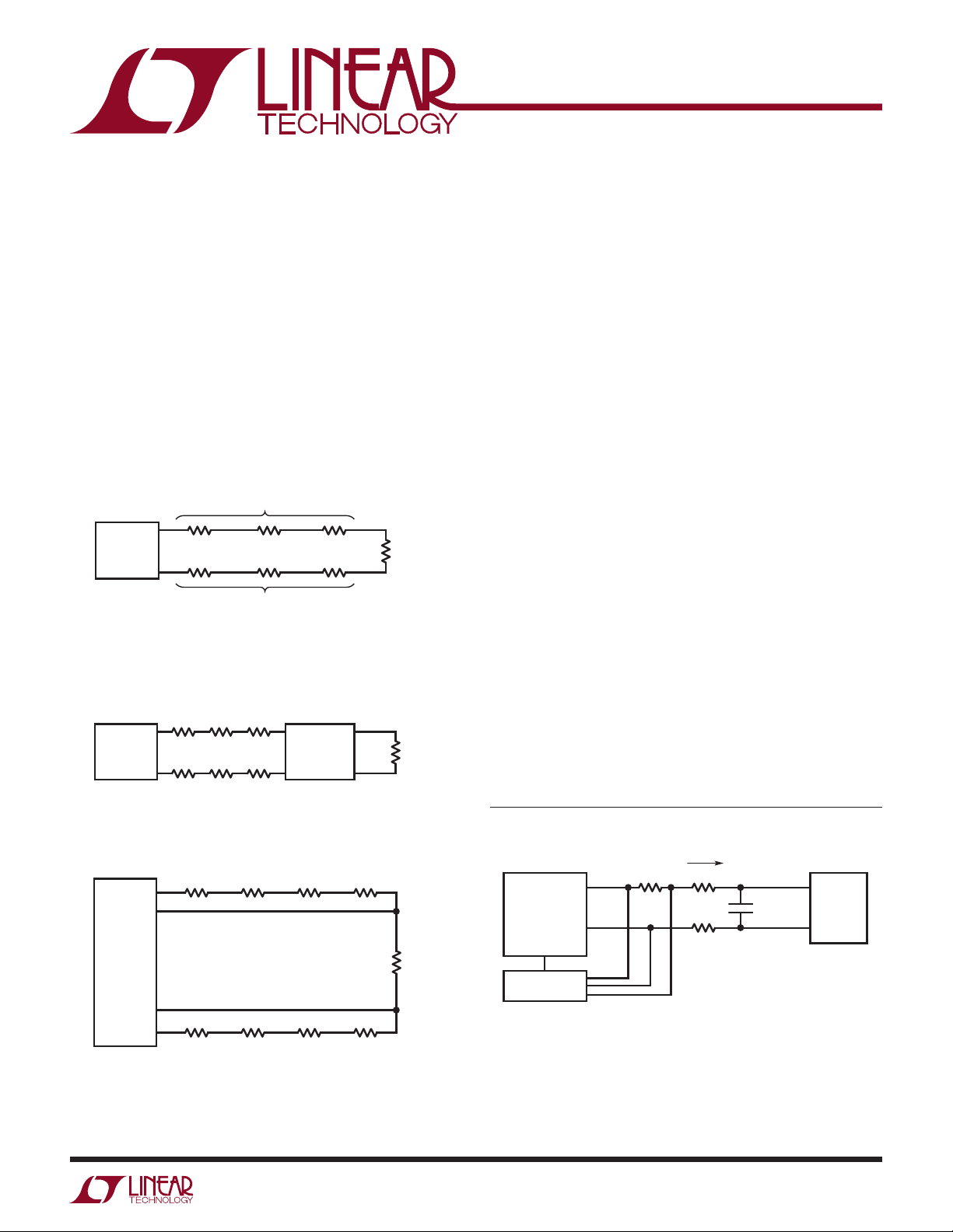
WIRING DROPS
POWER
SUPPLY
WIRING DROPS
Figure 1. Unavoidable Wiring Drops Cause Low Load
Voltage. Line and Load Resistance Variations Introduce
Additional Load Voltage Uncertainty, Mitigating Against
Compensation by Raising Supply Voltage
POWER
SUPPLY
LOAD
VOLTAGE
REGULATOR
Figure 2. Local Regulation Stabilizes
Load Voltage But is Ineffi cient
V
SENSE
POWER
SUPPLY
SENSE
V
OUT
OUT
VOLTAGE DROP R
+
+
–
VOLTAGE DROP R
–
WIRE
WIRE
Figure 3. Classical “4-Wire” Remote Sensing. V
Voltage Drops Are Compensated by Regulator Sensing at Load.
High Impedance Sense Inputs Negate Sense Wire Resistance.
Approach Requires Four Wires
AN125 F01
AN125 F02
OUT
LOAD
LOAD
LOAD
AN125 F03
Line
Figure 2 illustrates one compensatory approach. Locally
positioned regulation stabilizes load voltage against line
drops but is ineffi cient due to regulator losses. Figure 3,
the classical approach, utilizes “4-wire” remote sensing to
eliminate line drop effects. The power supply sense inputs
are fed from load referred sense wires. The sense inputs
are high impedance, negating sense line resistance effects.
This scheme works well, but requires dedicated sense
wires, a signifi cant disadvantage in many applications.
“Virtual” Remote Sensing
Figure 4 retains the advantages of classical 4-wire remote sensing while eliminating the sense leads. Here,
the LT4180 Virtual Remote Sense™ (VRS) IC alternates
output current between 95% and 105% of the nominal
required output current. The LT4180 forces the power
supply to provide a DC current plus a small square wave
current with peak-to-peak amplitude equal to 10% of the
DC current. Decoupling capacitor C
, normally required
LOAD
for low impedance under transient conditions in non-VRS
systems, takes an additional role by fi ltering out the VRS
square wave excursions.
L, LT, LTC, LTM, Linear Technology and the Linear logo are registered trademarks and Virtual
Remote Sense is a trademark of Linear Technology Corporation. All other trademarks are the
property of their respective owners.
SENSE
+
V
POWER SUPPLY
OUT
–
CONTROL PIN
LT4180
V
= DC + SQUAREWAVE FROM WIRING VOLTAGE DROP
OUT
REMOVES SQUAREWAVE, SO VL CONTAINS ONLY DC.
C
LOAD
= DC + SQUAREWAVE
I
L
Figure 4. LT4180 2-Wire Virtual Remote Sense Estimates
Wiring Voltage Drops, Compensates by Adjusting Supply
Output Voltage. Wiring Loss Is Determined by Measuring
Small Signal Square Wave Carrier Induced Voltage Drop.
Load Capacitor Absorbs Square Wave; Load Is at DC
R
R
WIRE
WIRE
I
L
/2I
+
V
C
L
/2
LOAD
LOAD
–
AN125 F04
an126fa
AN126-1
Page 2
Application Note 126
Because C is sized to produce an “AC short” at the square
wave frequency, a square wave voltage is produced at the
power supply equal to V
= 0.1 • IDC • R
OUTAC
WIREVP-P
. The
square wave voltage at the power supply has a peak-topeak amplitude equal to one tenth the DC wiring drop. This
is a direct measurement of wiring drop, not an estimate,
accurate over all load currents. Signal processing produces
a DC voltage from this AC signal which is introduced into
the supply feedback loop to provide accurate load regula-
1
. Note that the “power supply” may be an IC linear or
tion
switching regulator, a module or any other power source
capable of variable output. Power supplies can be synchronized to the LT4180 and VRS operating frequency is
adjustable over more than three decades. Optional spread
spectrum operation provides partial immunity from singletone interference and a 3V to 50V input range simplifi es
design. Because this technique is based on an estimate
of load voltage, not a direct measurement, the resultant
correction is an approximation, but a very good one.
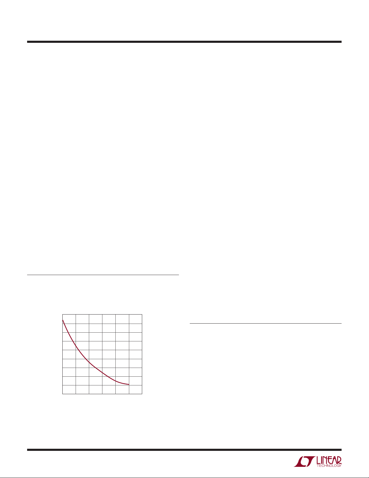
Typical LT4180 load regulation is plotted in Figure 5. In
this example, load current increases from zero until it
produces a 2.5V wiring drop. Load voltage drops only
73mV at maximum current. A voltage drop equivalent to
50% of load voltage results in only a 1.5% shift in load
voltage value. Smaller wiring drops produce even better
results.
Note 1. Readers fi nding their intellectual prowess unsatiated by this
admittedly cursory description will fi nd more studious coverage in
Appendix A, “A Primer on LT4180 VRS Operation.”
5.00
4.99
4.98
4.97
4.96
(V)
LOAD
4.95
V
4.94
4.93
4.92
4.91
0
0.5 1.51 2 2.5 3
V
(V)
WIRING
AN126 F05
Applications
The following applications are all VRS augmented voltage
regulators of various descriptions. The power regulation
stages employed are, with one exception, generic LTC
designs and are spared exhaustive commentary, permitting emphasis on the LT4180 VRS role. Additionally, the
similarity of the VRS associated circuitry across the broad
array of applications shown should be noted, and is indicative of the relative ease of implementation. Surprisingly
little change is needed to use the VRS in the different
situations presented.
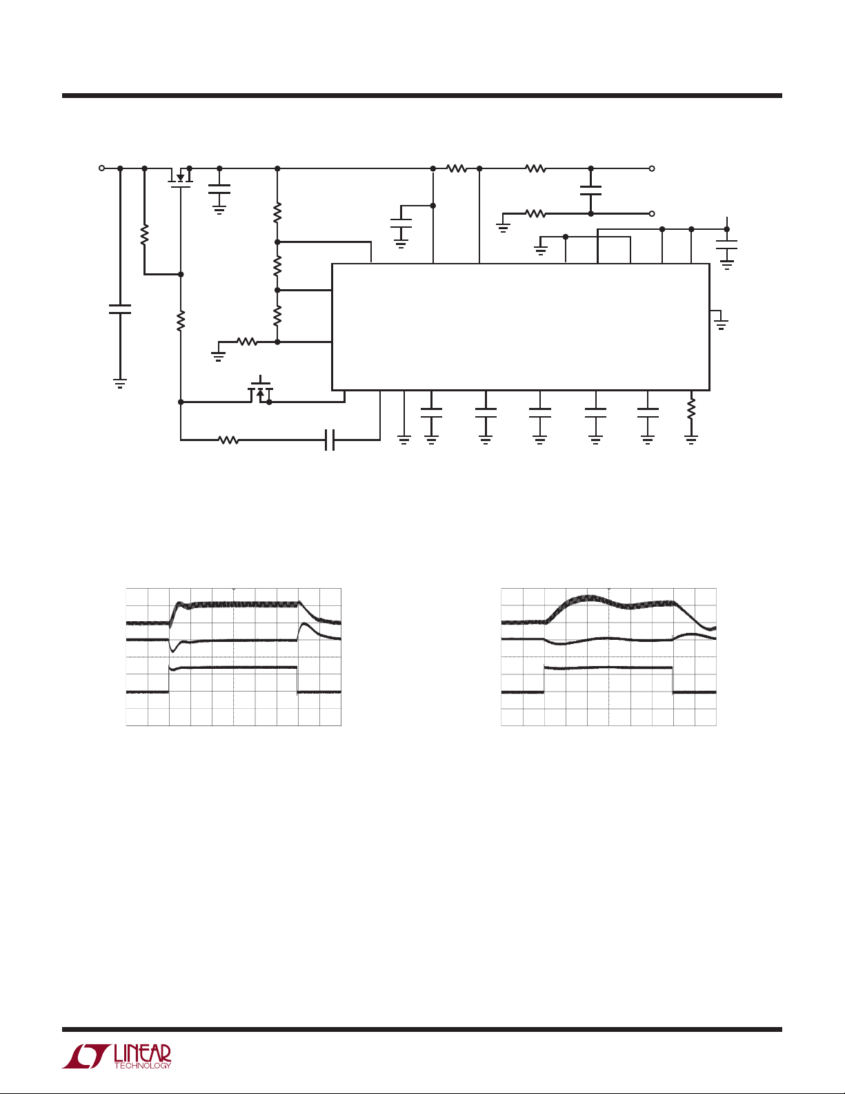
VRS Linear Regulators
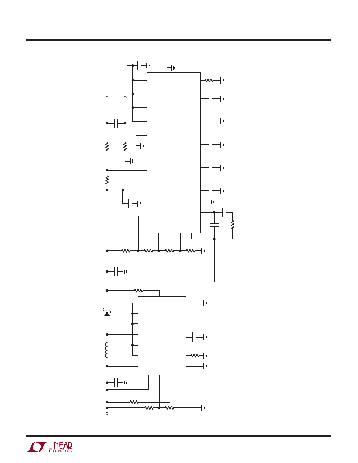
Figure 6 adds a simple stage to the LT4180 to implement
a complete VRS aided linear regulator. The LT4180 senses
current via the 0.2 shunt and feedback controls Q1 with
Q2, completing a control loop. Cascoded Q2 permits the
ICs 5V capable open drain output to control a high voltage
at Q1’s gate. Components at the compensation pin furnish
2
loop stability, promoting good transient response
shows Figure 6’s load step waveforms. They include V
(trace A), V
LOAD
(B) and I
(C). Transient response is
LOAD
. Figure 7
SENSE
determined by loop compensation, load capacitance and
remote sense sample rate. Figure 8 shows response with
increased to 1100µF. Load voltage transient excur-
C
LOAD
sion reduces and duration increases.
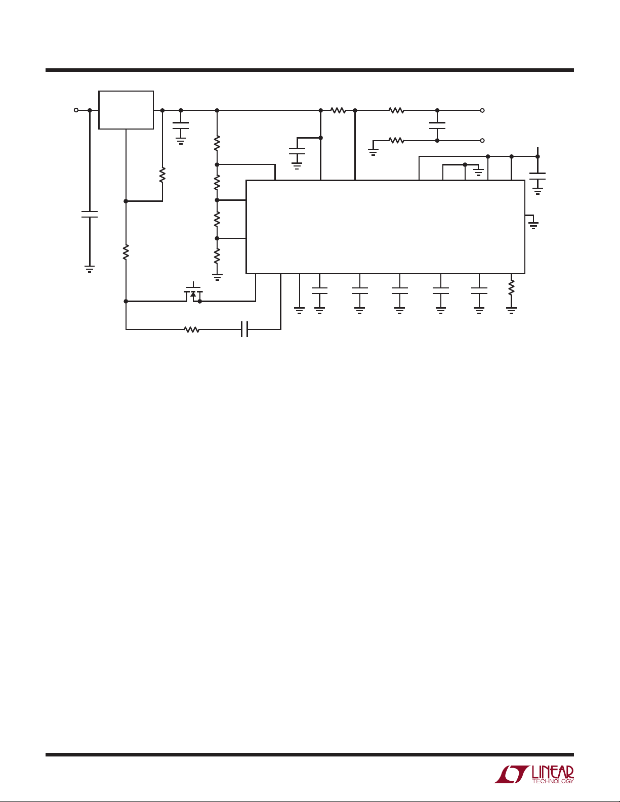
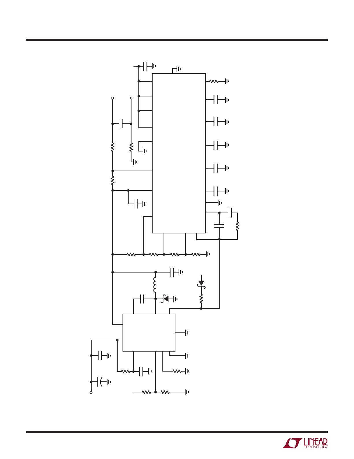
Figure 9, employing a monolithic regulator, adds current
limiting and simplifi es loop compensation. Transient response approximates Figure 6’s. As before, the LT4180’s
low voltage drain pin requires a cascode transistor to
control the high voltage at the LT3080 set pin.
Note 2. Value selection procedure for LT1480 VRS circuits is detailed in
Appendix B, “Design Guidelines for LT4180 VRS Circuits.”
Figure 5. Typical LT4180 Virtual Remote Sense Performance
Shows 1.6% Regulation vs 0V → 2.5V Wiring Drop
AN126-2
an126fa
Page 3
Application Note 126
V
20V
Q1
10µF
25V
IRLZ44
27k
10k
GUARD PINS NOT SHOWN
200k
4.7µF
5.36k
1%
Q2
INTV
VN2222
63.4k
1%
3.74k
1%
2.2k
1%
CC
330pF
RUN
FB
OV
COMP GNDDRAIN
IN
0.2
1%
1µF
SENSE
V
IN
CHOLD1 CHOLD2 CHOLD3 CHOLD4
WIRING DROP
LOAD RETURN
WIRING DROP
LT4180
470pF47nF
DIV2
100µF
33nF
LOAD VOLTAGE
12V, 500mA
8Ω TOTAL WIRING DROP
LOAD
RETURN
V
DIV0DIV1
PP
C
OSC
470pF470pF
INTV
SPREAD
R
OSC
CC
41.2k
1%
AN126 F06
INTV
CC
1µF
Figure 6. Virtual Remote Sense Controls Discrete Linear Regulator. Q2 Cascodes Drain Output,
Buffering High Voltage Q1 Gate Drive. COMP Pin Associated Components Stabilize Loop
A = 2V/DIV
B = 2V/DIV
AC COUPLED
C = 0.2A/DIV
ON 0.2A
DC LEVEL
5ms/DIV
AN126 F07
Figure 7. Figure 6’s Load Step Waveforms with 100μF Load
Capacitor Include V
(Trace A), V
SENSE
LOAD
(B) and I
LOAD
(C).
Transient Response is Determined by Loop Compensation,
Load Capacitance and Remote Sense Sample Rate
A = 2V/DIV
B = 2V/DIV
AC COUPLED
C = 0.2A/DIV
ON 0.2A
DC LEVEL
5ms/DIV
Figure 8. Same Conditions as Figure 7 with C
1100μF. V
Transient Excursion Reduces, Duration Extends
LOAD
LOAD
AN126 F08
Increased to
an126fa
AN126-3
Page 4
Application Note 126
V
18V
IN
LT3080
IN OUT
SET
10µF
25V
100k
GUARD PINS NOT SHOWN
10k
4.7µF
INTV
VN2222
51k
60.4k
1%
3.57k
1%
1.78k
1%
5.36k
1%
CC
1500pF
RUN
FB
OV
COMP GNDDRAIN
0.2
1%
1µF
SENSE
V
IN
CHOLD1 CHOLD2 CHOLD3 CHOLD4
WIRING DROP
LOAD RETURN
WIRING DROP
DIV2
LT4180
470pF47nF
470µF
47nF
DIV0DIV1
LOAD VOLTAGE
12V, 500mA
4Ω TOTAL
WIRING DROP
LOAD
RETURN
V
PP
C
OSC
330pF470pF
INTV
SPREAD
R
OSC
CC
22.1k
1%
AN126 F06
INTV
CC
1µF
Figure 9. Figure 6’s Approach Utilizing IC Regulator Adds Current Limiting,
Simplifi es Loop Compensation. Transient Response Approximates Figure 6’s
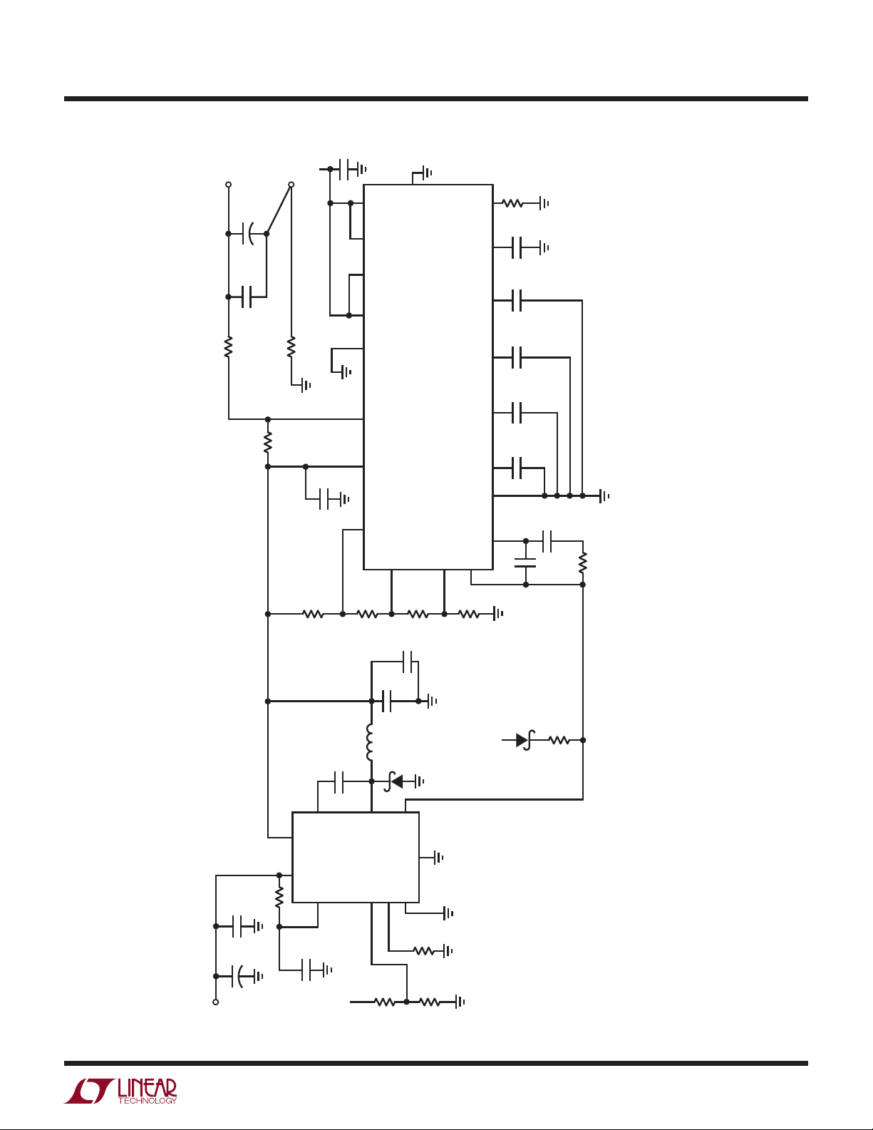
VRS Equipped Switching Regulators
VRS based switching regulators are readily constructed.
Figure 10’s fl yback voltage boost confi guration has similar
architecture to the linear examples although output voltage
is above the input. In this case, the LT4180 open drain output
is directly compatible with the LT3581 boost regulator low
voltage V
pin––no cascode stage is necessary.
C
Step down (“Buck”) VRS equipped switching regulators are
similarly easily achieved. Figure 11’s scheme, reminiscent
of the previously described linear regulators, substitutes
an LT3685 step down regulator which is directly controlled
from the LT4180 open drain output. A single pole roll-off
stabilizes the loop and a 12V, 1.5A output is maintained
from a 22V to 36V input despite a 0Ω to 2.5Ω wiring drop
loss. Figure 11A is similar, except that it provides a 5V, 3A
output from a 12V to 36V input.
VRS Based Isolated Switching Supplies
The VRS approach is adaptable to isolated output supplies.
Figure 12’s 24V output converter utilizes an approach
similar to the previous examples except that it supplies
a fully isolated output. The virtual remote sense feature
accommodates a 10Ω wire resistance. The LT3825 and T1
form a transformer coupled power stage. Opto-coupled
feedback maintains output isolation.
Figure 13’s 48V → 3.3V, 3A design also has a fully isolated
output, facilitated by power delivery through a transformer
and optically coupled feedback loop closure. The LT3758
drives T1 via Q1. T1’s rectifi ed and fi ltered secondary
supplies output power which is corrected for line drops
by the LT4180. Isolation is maintained by transmitting the
feedback signal with an opto-isolator. The opto-isolators
output collector ties back to the LT3578 V
pin, closing
C
the control loop.
AN126-4
an126fa
Page 5
OV
FB
DIV0DIV1
V
IN
INTV
CC
INTV
CC
V
PP
COMP GND
DRAIN
DIV2
CHOLD1 CHOLD2 CHOLD3 CHOLD4
47nF
AN126 F10
RUN
R
OSC
C
OSC
40.2Ω
1%
SENSE
SPREAD
LT4180
470pF470pF
470pF47nF
10nF
1µF
41.7k
1%
73.2Ω
1%
1.24k
1%
24.3k
1µF
0.2
1%
WIRING DROP
VIN5V
LOAD VOLTAGE
12V, 500mA
(100mA MIN.)
6Ω TOTAL WIRING DROP
LOAD
RETURN
10µF
25V
4.7µF
16V
L1
4.7µH
DFLS220
LOAD RETURN
WIRING DROP
100µF
191k
100k
10k
107Ω
1%
47pF
15k
LT3581
SW2SW2SW2SW1SW1SW1GATE
RT SSSYNC GND
V
CC
SHDN
FAULT
FB
VC
84.5k
0.1µF
L1 = VISHAY IHLPI525CZ-11
GUARD PINS NOT SHOWN
+
–
Application Note 126
Pin
C
Figure 10. Virtual Remote Sensed Voltage Boost Confi guration.
LT4180 Drain Output Controls Flyback Regulator via LT3581 V
an126fa
AN126-5
Page 6
Application Note 126
12V, 1.5A
2.5Ω TOTAL
WIRING DROP
CC
INTV
LOAD
RETURN
1µF
AN126 F11
22.1k
R
C
1%
OSC
330pF470pF
OSC
CC
INTV
SPREAD
PP
V
470µF
WIRING DROP
LOAD RETURN
0.067 WIRING DROP
61.9k
1%
DIV0DIV1
DIV2
LT4180
SENSE
IN
V
1µF
RUN
22µF
2k
25V
1%
OV
DRAIN
5.36k
1%
3.65k
FB
1%
CHOLD1 CHOLD2 CHOLD3 CHOLD4
COMP GND
CC
INTV
47pF
47nF
470pF47nF
3.3nF
28k
Step-Down
IN
to 36V
IN
AN126-6
1µF
22µF
+
IN
V
22V TO 36V
50V
50V
BD
IN
V
100k
INTV
CC
0.47µF
BOOST
RUN/SD
0.1µF
LT3685
50V
30.1k
10µH
SW
FBRTSYNC
DFLS240
VC
GND
10k
68.1k
1%
CMDSH-3
1k
Regulator Maintains 12V Output Despite Wiring Losses
Figure 11. Remote Sense Corrected 22V
L1 - VISHAY IHLP2020CZ-11
GUARD PINS NOT SHOWN
an126fa
Page 7
OUT
5V, 3A
0.4Ω TOTAL
WIRING DROP
V
C2
470µF
10V
+
C1
470µF
10V
+
–
WIRING DROP
1%
0.033Ω
CC
LOAD
RETURN
INTV
WIRING DROP
LOAD RETURN
Application Note 126
1µF
AN126 F11A
22.1k
CC
INTV
SPREAD
PP
V
DIV0
DIV1
DIV2
LT4180
SENSE
IN
V
1µF
OSC
R
OSC
C
CHOLD1 CHOLD2 CHOLD3 CHOLD4
1%
330pF
47nF
470pF
470pF47nF
4.7µF
50V
100k
BD
V
IN
21.5k
1%
BOOST
RUN/SD
1.87k
6.8µH
0.47µF
LT3693EDD
RUN
FB
2.15k
1%
47µF
10V
47µF
10V
MBRA340T3G
VC
SW
GND
FBRTSYNC
1%
OV
DRAIN
5.36k
1%
COMP GND
4.7nF
Step-Down Remote
OUT
47pF
CMDSH-3
CC
INTV
23.2k
1k
GUARD PINS NOT SHOWN
C1 = C2 = AVXTPSE477M010R0050
to 5V
IN
→ 36V
IN
Figure 11A. 12V
Sensed Regulator Has Similar Architecture to Figure 11
+
IN
V
8V TO 36V
22µF
50V
68.1k
1%
10k
1%
1%
an126fa
0.1µF
30.1k
CC
INTV
AN126-7
Page 8

Application Note 126
V
36V to 72V
T1
t
IN
4.7µH
+
V
IN
383k
1%
14k
1%
3.01k
1%
BAS21LT1
40.2k
1%
OPTIONAL
MMBT3906
+
10µF
100V
2.2µF
100V
–
V
IN
56pF
3.9k
1/4W
20
1/8W
33nF
+
68µF
20V
FB
OVLO
OSCAP ROCMPPGOLYENOL CMPC TON
38.3k
*
3.9k
1/4W
10k
56pF
56pF
0.1µF
SYNCSFST
30k
0.022µF
LT3825
2.05k
130k
1%
47k
1/4W
12.3V TO 16.5V
CC
0.1µF
–V
OUT
1µF
50V
+V
CC
100k
PGV
SGND/
PGND
SENP
SENN
VC
220pF
0.2
1%
30k
1nF
68pF
250V
47k
1/4W
Si7302DN
0.05
1206
R
WIRE
–V
OUT
ES1G
tt
tt
t
4.7nF
250V
V
OUT
24V, 500mA
10Ω TOTAL WIRING DROP
+
220µF
35V
LOAD RETURN
200
1/4W
10µF
35V
30pF
500V
100µF
35V
10µF
35V
LOAD RETURN
WIRING DROP
INTV
CC
1.37k
* 12mA MINIMUM
LOAD REQUIREMENT
+V
CC
12k
1k
MMBT3908
10µF TANYO YUDEN GMK325BJ106KN 1210
100µF 36V NICHICON PL (M)
10µF 100V SANYO 100CE10FS
68µF 20V KEMET T491D686K020AS
4.7nF 250V MURATA GA343DR7GD472KW01L
4.7µH COOPER BUSSMANN SO3814-4R7-R
1/4W RESISTORS ARE 1206
1/8W RESISTORS ARE 0805
T1 PULSE PA2925NL
GUARD PINS NOT SHOWN
6.8k
MOC207
2k
INTV
VN2222
1%
1.58k
1%
5.36k
1%
–V
OUT
CC
= INPUT COMMON
Figure 12. Virtual Remote Sensed, Isolated 36VIN → 72VIN to 24V
FB
OV
DRAIN
47pF
330pF
10k
1%
RUN
V
COMP GND
SENSE
IN
CHOLD1
Converter Accommodates
OUT
DIV2
LT4180
CHOLD2 CHOLD3 CHOLD4
0.047µF
3.3nF
3.3nF
V
DIV0DIV1
PP
C
OSC
0.1µF
10Ω Lead Wire Resistance. LT3825/T1 Form Transformer Coupled Power Stage. LT4180 Provides
Virtual Remote Sense, Opto-Coupled Feedback Maintains Output Isolation
INTV
SPREAD
R
470pF
CC
OSC
41.7k
1%
1µF
AN126 F12
–V
OUT
AN126-8
an126fa
Page 9

3.3V, 3A
+
0.4 TOTAL WIRING DROP
LOAD
RETURN
*
LOAD
C
Application Note 126
1µF
CC2
INTV
CC
INTV
PP
V
DIV0DIV2
SPREAD
R
C
OSC
470pF
OSC
41.2k
0.1µF
1%
AN126 F13
0.4
WIRING DROP
1%
0.033
T1
WIRING DROP
LOAD RETURN
1µF
13k
100µF
10V
w2
UPS840
ttt
1%
DIV1
SENSE
IN
V
RUN
523Ω
INTV
1%
CC2
470pF
LT4180
OV
FB
2.74k
1.3k
0.01µF
1%
DRAIN
5.36k
1%
CHOLD2 CHOLD3 CHOLD4
47nF
CHOLD1
COMP GND
47pF
PS2801-1
470pF
0.015µF
1%
10.7k
1M
2200pF
Figure 13. 48V → 3.3V Isolated Step-Down, Remote Sensed
Regulator. T1 Delivers Isolated Power, LT4180 Remotely
Senses Output, Supplies Feedback via Opto-Isolator
an126fa
1µF
1µF
IN
V
18V TO 72V
BAV21W
10k
4700pF
100V
100V
4.7µF
BAS516
51
50V
9.1k
Si4848DV
1Ω
1µF
IN
V
RCS1
0.033
100Ω
= INPUT COMMON
CC
GATE
SYNC
SENSE
INTV
IN
V
LTC3758
SS
VC
105k
1%
SHDN/UVLOFBRT
8.66k
1%
GND
36.5k
1%
= OUTPUT COMMON
= 4×, 470µF
LOAD
T1 = PULSE ENERGY PA1277NL
GUARD PINS NOT SHOWN
* C
AVXTPSE477M010R0050
AN126-9
Page 10

Application Note 126
Figure 14, also a VRS isolated step-down supply, uses a
commercially produced 48V isolated input module augmented with virtual remote sensing. The module sense
terminals are unused. The LT4180 wiring drop correction
is introduced at the module trim pin. Component values
are shown for 3.3 and 5V outputs. The “black box” Vicor
module trim pin transient response defi nes available control
bandwidth. Figure 15, trace A, is the trim pin input step
(see test circuit A), trace B, the module output. The trim
pin directed dynamics set practical expectations for VRS
equipped loop response around the module. Figures 16
and 17 do not disappoint. Figure 14’s load step response
appears in Figure 16. Trace A is load step current, trace B,
the resultant output voltage transient. The response envelope, bounded by module trim pin dynamics, is clean and
well controlled. Figure 17 shows Figure 14’s turn-on into
a 2.5Amp load. LT4180 activation arrests the initial abrupt
rise at the 3rd vertical division. The ascent’s conclusion
is controlled to the regulation point in damped fashion.
1µF
13.3k/
17.4k
LT4180 sampling square wave residue is just discernible
in the waveforms settled portion.
BEFORE PROCEEDING ANY FURTHER, THE READER
IS WARNED THAT CAUTION MUST BE USED IN THE
CONSTRUCTION, TESTING AND USE OF THIS CIRCUIT.
HIGH VOLTAGE, AC LINE CONNECTED POTENTIALS
ARE PRESENT IN THIS CIRCUIT. EXTREME CAUTION
MUST BE USED IN WORKING WITH AND MAKING CONNECTIONS TO THIS CIRCUIT. REPEAT: THIS CIRCUIT
CONTAINS DANGEROUS, AC LINE CONNECTED HIGH
VOLTAGE POTENTIALS. USE CAUTION.
Figure 18’s VRS aided “Off-Line” isolated output supply
has a 5V output with 2A capacity. The schematic appears
complex, but inspection reveals it to be essentially an AC
line powered variant of Figure 13’s isolated approach. The
LT4180 provides remote sensing and closes an isolated
feedback loop with optical transmission.
0.04
WIRING DROP
LOAD RETURN
WIRING DROP
+
3.3V/2.5A
5V/2A
0.4Ω TOTAL WIRING DROP
2200µF
LOAD
RETURN
523Ω/
4.64k
2.4k
48V
V
V
IN+
VI-230-EX
IN–
V
IN+
V
IN–
VICOR
MODULE
V
OUT+
V
SEN+
TRIM
V
SEN–
V
OUT–
2.74k/
1.69k
5.36k/
5.36k
10k
GUARD PINS NOT SHOWN
FB
OV
DRAIN
47pF
240k
RUN
V
COMP GND
IN
4.7nF
CHOLD1
SENSE
CHOLD2 CHOLD3 CHOLD4
0.047µF
DIV2
LT4180
3.3nF
DIV0DIV1
3.3nF
0.1µF
INTV
V
C
OSC
PP
1nF
SPREAD
R
OSC
CC
42.2k
1%
AN126 F14
1µF
Figure 14. Commercially Produced, Isolated 48V Input Module Augmented with
Virtual Remote Sense. Module Sense Terminals Are Unused. Wiring Drop Correction
Introduced at Module Trim Pin. Component Values Shown for 3.3V/5V Outputs
AN126-10
an126fa
Page 11

A = 5V/DIV
B = 0.5V/DIV
ON 5VDC
A = 2A/DIV
ON 1A DC
Application Note 126
48V
IN4148
24k
48V
RETURN
Trim Pin Pulse Test Circuit
5ms/DIV
PULSE
GENERATOR
AN126 F15
Figure 15.Vicor Module Trim Pin Transient Response Defi nes Available Control Bandwidth.
Trace A is Trim Pin Input Step (See Test Circuit), Trace B, Module Output
1V/DIV
TRIM
VICOR
VI-230-EX
SEN
SEN
+
V
LOAD
–
V
B = 0.2V/DIV
20ms/DIV
AN126 F16
Figure 16. Figure 14’s Load Step Response. Trace A is
Load Step Current, Trace B Resultant Output Voltage
Transient. Response Envelope, Bounded by Module
Trim Pin Dynamics, is Well Controlled
VRS Halogen Lamp Drive Circuit
A fi nal circuit, Figure 19, uses the VRS to stabilize drive to
a halogen lamp, in this case a 12V, 30W automotive type.
Lamp output power remains constant despite 9V to 15V
input variation and line resistance/connection uncertainties. Additional benefi ts include constant color output and
extended lamp life. The circuit, a step up/down (“SEPIC”)
converter, maintains 12V at the lamp despite the 9V to 15V
3
input range
. The VRS functions in the manner previously
described. Line resistance losses due to switches, wiring
and connectors are obviated by VRS action. Figure 20
plots unaided vs remote sensed and regulated halogen
lamp light output. VRS equipped luminosity is fl at over
the 9 to 15V input range while unregulated performance
Note 3. SEPIC operation is described in Reference 2.
20ms/DIV
AN126 F17
Figure 17. Figure 14’s Turn-On into a 2.5A Load. LT4180
Activation Arrests Initial Abrupt Rise at Third Vertical Division.
Ascent Conclusion is Controlled to Regulation Point. LT4180
Sampling Square Wave Residue is Discernible
suffers dramatically. The regulation also benefi ts lamp
life by greatly reducing lamp turn-on current. Figure 21
shows unregulated lamp turn-on exceeding 20A without
regulation. In Figure 22, regulation cuts current peaking
to 7A, a 3x reduction. This soft turn-on and constant 12V
drive under high/low line conditions optimizes illumination
and improves lamp life.
References
1. LT4180 Data Sheet, Linear Technology Corporation,
2010.
2. Ridley, R. “Analyzing the Sepic Converter”, Power
Systems Design Europe, November, 2006.
an126fa
AN126-11
Page 12

Application Note 126
200pF
IN
V
200V
62
6mH
RT1
30pF
DF06M
t
500V
200V
47µF
+
470k
T1
P6KE200A
400V
1/4W
220
150µF
+
10µF
1µH
270µF
+
MBR20200CT
7T70T
t
510
2W
MUR160E
470k
1/4W
t
1/4W
16V
16V
16V
t
BAS21
2.2nF
IN
V
12Ω
250VAC “Y”
OUT
* V
5V, 2A
0.05Ω
17T
270k
+
WIRE
R
1%
t
1/4W
270k
1/4W
1.2Ω
SPB03N60C3
IN
V
CC
INTV
2200µF
1Ω TOTAL
WIRING DROP
10µF
16V
20.5k
2N7002
1/4W
200k
1/2W
1%
1k
13V
200k
4.53k
CC
INTV
3.9
2N3904
1k
CMPZ5243B
1/2W
1µF
CC
INTV
PP
V
DIV0DIV1
DIV2
SENSE
IN
V
RUN
1%
CC
V
FB
0.47µF
150µF
+
OUT
REF
V
CC
V
18k
SPREAD
2.67k
750Ω
16V
SEN
I
VCCFB
LT4180
1%
LT1241
OV
CNY17-3
COMP
5.36k
150pF
RT/CT
DRAIN
1%
12nF
GND
0.1µF
OSC
R
OSC
C
CHOLD1 CHOLD2 CHOLD3 CHOLD4
COMP GND
1µF220pF
41.2k
0.047µF
3.3nF
100pF
1%
AN126 F11
470pF
3.3nF
10nF
0.1µF
6.8k
1M
* 100mA MINIMUM LOAD REQUIRED.
NOTE:
47µF 400V CHEMICON EKXG401ELL470ML25S
2200µF 10V SANYO 10MV2200AX
150µF 16V SANYO 16MV150AX
270µF 16V SANYO 16SEPC270M
10µF 16V TDK C3225X7RK106M
1µH VISHAY IHLP2525CZER1ROM
6mH PANASONIC ELF11M030E
2
Figure 18. A 5V Output “Off-Line” Converter Equipped with Virtual Remote Sense.
LT4180 Provides Remote Sensing, Closes Isolated Feedback Loop via Opto-Isolator
WARNING! SCREENED AREA CONTAINS LETHAL AC LINE CONNECTED HIGH
VOLTAGES. USE CAUTION IN CONSTRUCTION AND TESTING.
RT1 CANTHERM MF72-33D7
T1 PULSE PA3072NL EF20 AL = 100nH/T
DANGER!! HIGH VOLTAGE!!
AN126-12
IN
0.1µF
250VAC “X”
= AC LINE COMMON
SCREENED AREA CONTAINS LETHAL
HIGH VOLTAGES! USE CAUTION IN
90V to 264VAC
CONSTRUCTION AND TESTING!
= OUTPUT COMMON
GUARD PINS NOT SHOWN
an126fa
Page 13

Application Note 126
1µF
12V, 30W
HALOGEN LAMP
1000µF
25V
+
LOAD RETURN
WIRING DROP
1%
0.04
1 CONNECTOR/SWITCH
WIRING DROP
1µF
SPREAD
CC
INTV
PP
V
DIV0DIV1
DIV2
SENSE
IN
V
RUN
42.2k
OSC
LT4180
FB
OV
DRAIN
OSC
R
OSC
C
CHOLD1 CHOLD2 CHOLD3 CHOLD4
COMP GND
47pF
1%
150pF470pF
0.1µF
470pF47nF
47nF
13.7k
1%
AN126 F19
0.1µH
PDS1045
50V
10µF
6.8µH
IN
V
9V TO 15V
84.5k
C2X
10µF
20V
++
22µF
25Vw3CERAMIC
50V
10µF
10µF
63V
+
6.8µF
50V
1%
200k
6.8µH
4.99k
43.2k
1%
42.2k
1%
IN
V
SHDN/UVLO
CC
INTV
3.4k
1%
4.7µF
10V
4.12k
LT3757
SS
1%
Q1
Si7850DP
GATE
0.1µF
6.65k
1%
SENSE
SYNC
6.8k
0.005
RT FBX VCGND
1W
42.2k10k
100pF
Figure 19. LT4180 Step Up/Down Converter Stabilizes 12V Drive to 30W Halogen
Automotive Lamp Despite 9V → 15V Input Variation and Line Resistance Uncertainties
GUARD PINS NOT SHOWN
IHLP4040DZR6R8M11 = 6.8µH
UMK325Bd106MM-T = 10µF, 50V
TMKBd226MM-T = 22µF
C2X = ZOSVPIO
IHLP1616ABERR10M01 = 0.1µH
an126fa
AN126-13
Page 14

Application Note 126
2
KILOCANDLES/M
Figure 20. Unaided vs Remote Sensed/Regulated Halogen Lamp Light
Output. Regulation Benefi ts Include Stable Illumination, Constant Color
Output and Extended Lamp Life
14.5
14.0
12.0
10.0
8.0
6.0
2.0
4.0
WITHOUT VIRTUAL REMOTE
SENSE/REGULATOR
WITH VIRTUAL REMOTE
SENSE/REGULATOR
0
9
10 1211 13 14 15
BATTERY VOLTAGE (V)
AN126 F20
A = 5A/DIV
50ms/DIV
Figure 21. Lamp Turn-On Current Exceeds 20A
Without Regulation, Degrading Lifetime
AN126 F21
A = 5A/DIV
50ms/DIV
AN126 F22
Figure 22. Regulation Promotes Soft Turn-On, 12V Drive
Under High/Low Line Conditions, Optimizing Illumination
and Improving Lamp Life
AN126-14
an126fa
Page 15

APPENDIX A
A Primer on LT4180 VRS Operation
Application Note 126
Voltage drops in wiring can produce considerable load
regulation errors in electrical systems (Figure A1). As load
current I
increases and the voltage delivered to the system (V
increases, voltage drop in the wiring (IL • RW)
L
)
L
drops. The traditional approach to solving this problem,
remote sensing, regulates the voltage at the load, increasing the power supply voltage (V
) to compensate for
OUT
voltage drops in the wiring. While remote sensing works
well, it does require an additional pair of wires to measure
at the load, which may not always be practical.
The LT4180 eliminates the need for a pair of remote sense
wires by creating a virtual remote sense. Virtual remote
sensing is achieved by measuring the incremental change
in voltage that occurs with an incremental change in current
in the wiring (Figure A2). This measurement can be used
to infer the total DC voltage drop in the wiring, which can
then be compensated for. The Virtual Remote Sense takes
AN125 A1
FB
),
over control of the power supply via its feedback pin (V
maintaining tight regulation of load voltage V
I
L
POWER SUPPLY
+
V
OUT
–
REMOTE SENSE WIRING
RW
POWER WIRING
.
L
SYSTEM
+
V
L
–
Figure A3 shows the timing diagram for Virtual Remote
Sensing (VRS). A new cycle begins when the power
supply and VRS close the loop around V
= H). Both V
V
OUT
OUT
and I
slew and settle to a new
OUT
(Regulate
OUT
value, and these values are stored in the Virtual Remote
Sense (Track V
OUTHIGH
= L and Track I
= L). The V
OUT
OUT
feedback loop is opened and a new feedback loop is set
up commanding the power supply to deliver 90% of the
previously measured current (0.9 I
OUT
). V
drops to a
OUT
new value as the power supply reaches a new steady state,
and this information is also stored in the Virtual Remote
Sense. At this point, the change in the output voltage
(∆V
) for a –10% change in output current has been
OUT
measured and is stored in the Virtual Remote Sense. This
voltage is used during the next VRS cycle to compensate
for voltage drops due to wiring resistance.
I
L
POWER SUPPLY
V
V
FB
VIRTUAL
REMOTE SENSE
OUT
I
SENSE
+
–
RW
POWER WIRING
+
–
V
L
SYSTEM
AN125 A2
Figure A1. Traditional Remote Sensing Works Well
But Requires Two Sense Wires
V
OUT
REGULATE V
TRACK V
REGULATE I
TRACK V
OUTHIGH
TRACK I
OUT
OUT
TRACK DV
OUT
OUT
LOW
LOW
OUT
Figure A3. Simplifi ed Virtual Remote Sense Timing
Diagram. State Machine Driven Sequence Samples
and Stores Information Necessary to Set Appropriate
Power Supply Voltage to Correct for Wiring Losses
Figure A2. Virtual Remote Sensing Eliminates Sense Wires
AN126 A3
an126fa
AN126-15
Page 16

Application Note 126
APPENDIX B
Design Guidelines for LT4180 VRS Circuits
INTRODUCTION
The LT4180 is designed to interface with a variety of power
supplies and regulators having either an external feedback
or control pin. In Figure B1, the regulator error amplifi er
(which is a g
amplifi er) is disabled by tying its inverting
m
input to ground. This converts the error amplifi er into a
constant-current source which is then controlled by the
drain pin of the LT4180. This is the preferred method of
interfacing because it eliminates the regulator error amplifi er from the control loop which simplifi es compensation
and provides best control loop response.
REGULATOR
OR
I
TH
+
V
C
–
Figure B1. Nonisolated Regulator Interface
For proper operation, increasing control voltage should
correspond to increasing regulator output. For example,
in the case of a current mode switching power supply, the
control pin ITH should produce higher peak currents as
the ITH pin voltage is made more positive.
Isolated power supplies and regulators may also be used
by adding an opto-coupler (Figure B2). LT4180 output
voltage INTV
In situations where the control pin V
supplies power to the opto-coupler LED.
CC
of the regulator may
C
exceed 5V, a cascode may be added to keep the DRAIN
pin of the LT4180 below 5V (Figure B3). Use a Low VT
MOSFET for the cascode transistor.
LT4180
DRAIN
AN126 B1
AN126-16
REGULATOR
+
OPTO-COUPLER
V
C
INTV
CC
LT4180
–
DRAIN
AN126 B2
Figure B2. Isolated Power Supply Interface
TO V
C
COMP
LT4180
INTV
CC
DRAIN
AN126 B3
Figure B3. Cascoded DRAIN Pin for Isolated Supplies
an126fa
Page 17

DESIGN PROCEDURE
The fi rst step in the design procedure (Figure B4) is to
determine whether the LT4180 will control a linear or
switching supply/regulator. If using a switching power
supply or regulator, it is recommended that the supply be
synchronized to the LT4180 by connecting the OSC pin to
the SYNC pin (or equivalent) of the supply.
If the power supply is synchronized to the LT4180, the
power supply switching frequency is determined by:
f
=
OSC
Recommended values for R
4
R
OSC•COSC
are between 20k and 100k
OSC
(with 30.1k the optimum for best accuracy) and greater
. C
than 100pF for C
OSC
may be reduced to as low as
OSC
50pF, but oscillator frequency accuracy will be somewhat
degraded.
The following example synchronizes a 250kHz switching
power supply to the LT4180. In this example, start with
= 30.1k:
R
OSC
C
=
OSC
250kHz • 30.1k
4
= 531pF
This example uses 470pF. For 250kHz:
R
=
OSC
250kHz • 470pF
4
= 34.04k
Application Note 126
LT4180 DESIGN FLOW
LINEAR
WHAT TYPE OF POWER
SUPPLY/REGULATOR?
f
= 2MHz, UNLESS SYSTEM
OSC
REQUIRES ANOTHER FREQUENCY
CALCULATE f
RESPONSE TIME OR CABLE PROPAGATION TIME
D
= f
RATIO
HIGHER FREQUENCY DIVISION RATIO
(TABLE 1, DATA SHEET)
CALCULATE ACTUAL f
SELECTED DIVISION RATIO
USE ACTUAL f
AND C
HOLD1–3
CALCULATE FEEDBACK, UNDER AND
OVERVOLTAGE RESISTOR NETWORK
BUILD PROTOTYPE, ADJUST POWER SUPPLY
COMPENSATION USING LOAD STEP TESTING
WITH SPREAD SPECTRUM OFF
START
FROM POWER SUPPLY
DITHER
TO COMPUTE C
DITHER
, SET C
. USE NEAREST
OSC/fDITHER
DITHER
HOLD4
SWITCHING
IS SUPPLY
NO
SYNCHRONIZED
TO LT4180?
f
= SWITCHING
OSC
SUPPLY FREQUENCY
USING
,
LOAD
= 1µF
YES
The closest standard 1% value is 34k.
The next step is to determine the highest practical dither
frequency. This may be limited either by the response
time of the power supply or regulator, or by the propagation time of the wiring connecting the load to the power
supply or regulator.
ADJUST C
TRY SPREAD SPECTRUM IF NARROW BAND
FOR PROPER VRS RESPONSE
HOLD4
INTERFERENCE IS ANTICIPATED
DONE
Figure B4. Design Flow Chart
AN126-17
AN126 B4
an126fa
Page 18

Application Note 126
First determine the settling time (to 1% of fi nal value)
of the power supply. The settling time should be the
worst-case value (over the whole operating envelope: V
, etc.).
I
LOAD
F1 =
2•t
1
SETTLING
Hz
IN
,
For example, if the power supply takes 1ms to settle
(worst-case) to within 1% of fi nal value:
F1 =
1
2•1e–3
= 500Hz
Next, determine the propagation time of the wiring. In
order to ignore transmission line effects, the dither period
should be approximately twenty times longer than this.
This will limit dither frequency to:
V
F
Hz
F2 =
20 • 1.017ns/ft • L
where VF is the velocity factor (or velocity of propagation),
and L is the length of the wiring (in feet).
For example, assume the load is connected to a power
supply with 1000ft of CAT5 cable. Nominal velocity of
propagation is approximately 70%.
0.7
= 34.4kHz
F2 =
20 • 1.017e– 9 • 1000
After the dither frequency is determined, the minimum
load decoupling capacitor can be determined. This load
capacitor must be suffi ciently large to fi lter out the dither
signal at the load.
C
where C
R
WIRE
=
LOAD
R
WIRE
is the minimum load decoupling capacitance,
LOAD
is the minimum wiring resistance of one conductor of
the wiring pair, and f
2.2
•2• f
DITHER
DITHER
is the minimum dither frequency.
Continuing the example, our CAT5 cable has a maximum
9.38Ω/100m conductor resistance.
Maximum wiring resistance is:
R
R
= 2 • 1000ft • 0.305m/ft • 0.0938Ω/m
WIRE
= 57.2Ω
WIRE
With an oscillator tolerance of ±15%, the minimum
dither frequency is 414.8Hz, so the minimum decoupling
capacitance is:
C
LOAD
=
57.2Ω • 2 • 414.8Hz
2.2
= 46.36µF
This is the minimum value. Select a nominal value to account for all factors which could reduce the nominal, such
as initial tolerance, voltage and temperature coeffi cients
and aging.
The maximum dither frequency should not exceed F1 or
F2 (whichever is less):
f
< min (F1, F2).
DITHER
Continuing this example, the dither frequency should be
less than 500Hz (limited by the power supply).
With the dither frequency known, the division ratio can
be determined:
f
D
RATIO
=
OSC
f
DITHER
250,000
=
500
= 500
The nearest division ratio is 512 (set DIV0 = L, DIV1 =
DIV2 = H). Based on this division ratio, nominal dither
frequency will be:
f
DITHER
f
OSC
=
D
RATIO
250,000
=
512
= 488Hz
AN126-18
CHOLD Capacitor Selection and Compensation
CHOLD1
A 47nF capacitor will suffi ce for most applications. A
smaller value might allow faster recovery from a sudden
load change, but care must be taken to ensure full load
p-p ripple at this node is kept within 5mV:
CHOLD2 = CHOLD3 =
2.5nF
f
DITHER
(kHz)
For a dither frequency of 488Hz:
CHOLD2 = CHOLD3 =
2.5nF
0.488(kHz)
= 5.12nF
NPO ceramic or other capacitors with low leakage and dielectric absorption should be used for all HOLD capacitors.
Set CHOLD4 to 1µF. This value will be adjusted later.
an126fa
Page 19

Compensation
Start with a 47pF capacitor between the COMP and DRAIN
pins of the LT4180. Add an RC network in parallel with the
47pF capacitor, 10k and 10nF are good starting values.
Once the output voltage has been confi rmed to regulate at
the desired level at no load, increase the load current to the
100% level and monitor the wire current (dither current)
with a current probe. Verify the dither current resembles
a square-wave with the desired dither frequency.
If the output voltage is too low, increase the value of the
10k resistor until some overshoot is observed at the leading
edge of the dither current waveform. If the output voltage
is still too low, decrease the value of the 10nF capacitor
and repeat the previous step. Repeat this process until the
full load output voltage increases to within 1% below the
no load level. Refer to Figures B5a, B5b and B5c, which
show compensation of the 12V 1.5A Buck Regulator Application on the data sheet. Check for proper voltage drop
correction over the load range. The “dither current” should
have good half-wave symmetry. Namely, waveform should
have similar rise and fall times, enough settling time at top
and bottom and minimum to no over/undershoot.
Application Note 126
V
LOAD
11.9V
I
DITHER
50mA/DIV
OUT
AN126 B5c
with
20µs/DIV
Figure B5c. Dither Current and V
3.3nF, 28k Compensation 1.5A Load
Set Final Value of CHOLD4
Set the minimum value for CHOLD4, by performing a
transient load test of 30% to 60% of the load and set the
value of CHOLD4 to where a nicely damped waveform is
observed. Refer to Figures B6a and B6b for an illustration.
After all the CHOLD values have been fi nalized, check for
proper voltage drop correction and converter behavior
(start-up, regulation etc.), over the load and input voltage ranges.
V
LOAD
11.2V
I
DITHER
50mA/DIV
20µs/DIV
Figure B5a. Dither Current and V
10nF, 10k Compensation 1.5A Load
V
LOAD
11.9V
I
DITHER
500mA/DIV
20µs/DIV
Figure B5b. Dither Current and V
10nF, 37k Compensation 1.5A Load
OUT
OUT
AN126 B5a
with
4180 F07b
with
V
LOAD
1V/DIV
I
DITHER
500mA/DIV
10ms/DIV
AN126 B6a
Figure B6a. 500mA to 1A Transient Response
Test with CHOLD4 = 25nF CHOLD4 Too Small
V
LOAD
1V/DIV
I
DITHER
500mA/DIV
10ms/DIV
AN126 B6b
Figure B6b. 500mA to 1A Transient Response Test
with CHOLD4 = 47nF Nicely Damped Behaviour
an126fa
AN126-19
Page 20

Application Note 126
Setting Output Voltage, Undervoltage and Overvoltage
Thresholds
The RUN pin has accurate rising and falling thresholds
which may be used to determine when Virtual Remote Sense
operation begins. Undervoltage threshold should never
be set lower than the minimum operating voltage of the
LT4180 (3.1V).
The overvoltage threshold should be set slightly greater
than the highest voltage which will be produced by the
power supply or regulator:
V
OUT(MAX)
V
OUT(MAX)
= V
LOAD(MAX)
should never exceed 1.5 • V
+ V
WIRE(MAX)
LOAD
Since the RUN and OV pins connect to MOSFET input
comparators, input bias currents are negligible and a common voltage divider can be used to set both thresholds
(Figure B7).
V
R1
R2
R3
R4
IN
LT4180
RUN
FB
OV
AN126 B5
R
SERIES
R1= R
R3 =
R2 = R
Where V
⎛
1.22 • R
=
⎜
V
⎝
UVL
−R
T
SERIES
⎛
1.22V − V
SERIES
UVL
⎜
OUT(NOM)
⎝
V
OUT(NOM)
−R3
is the RUN voltage and V
−R4
R
⎞
T
−R4
⎟
⎠
R4
•
R
T
nominal output voltage desired.
For example, with V
RT=
7.5V
= 4V, VOV = 7.5V and V
UVL
= 37.5k
200µA
R4 =
1.22V
= 6.1k
200µA
R
SERIES
⎛
1.22V • 37.5k
=
⎜
⎝
4V
⎞
− 6.1k = 5.34k
⎟
⎠
R1 = 37.5k −5.34k −6.1k = 26.06k
⎞
⎟
⎠
T
OUT(NOM)
is the
OUT(NOM)
= 5V,
Figure B7. Voltage Divider for UVL and OVL
The voltage divider resistors can be calculated from the
following equations:
RT=
V
OV
200µA
,R4=
1.22V
200µA
where RT is the total divider resistance and VOV is the
overvoltage set point.
Find the equivalent series resistance for R2 and R3 (R
SERIES
).
This resistance will determine the RUN voltage level.
AN126-20
R3 =
1.22V −
⎛
5V • 6.1k
⎜
37.5k
⎝
5V
⎞
⎟
⎠
= 3.05k
37.5k
R2 = R
SERIES
−R3 = 2.29k
R
Select the value of R
SENSE
SELECTION
so that it produces a 100mV volt-
SENSE
age drop at maximum load current. For best accuracy, V
and SENSE should be Kelvin connected to this resistor.
an126fa
IN
Page 21

Application Note 126
Soft-Correct Operation
The LT4180 has a soft-correct function which insures
orderly start-up (Figure B8). When the RUN pin rising
threshold is fi rst exceeded (indicating V
has crossed
IN
its undervoltage lockout threshold), power supply output
voltage is set to a value corresponding to zero wiring voltage drop (no correction for wiring). Over a period of time
(determined by C
), the power supply output voltage
HOLD4
ramps up to account for wiring voltage drops, providing
best load-end voltage regulation. A new soft-correct cycle
is also initiated whenever an overvoltage condition occurs.
10V
5V
200ms/DIV
HOLD4
AN126 B8
= 1μF
POWER SUPPLY
OUTPUT VOLTAGE
POWER SUPPLY
INPUT VOLTAGE
Figure B8. Soft-Correct Operation, C
substantial leakage current through the leakage resistance
). By adding a guard ring driver with approximately
(R
LKG
the same voltage as the voltage on the hold capacitor node,
the difference voltage across R
is reduced substantially
LKG1
thereby reducing leakage current on the hold capacitor.
Synchronization
Linear and switching power supplies and regulators may
be used with the LT4180. In most applications regulator
interference should be negligible. For those applications
where accurate control of interference spectrum is desirable, an oscillator output has been provided so that
switching supplies may be synchronized to the LT4180
(Figure B10). The OSC pin was designed so that it may
directly connect to most regulators, or drive opto-isolators
(for isolated power supplies).
REGULATOR
LT4180
OSCSYNC
AN126 B10
Using Guard Rings
The LT4180 includes a total of four track/holds in the
Virtual Remote Sense path. For best accuracy, all leakage
sources on the CHOLD pins should be minimized.
At very low dither frequencies, the circuit board layout
may include guard rings which should be tied to their
respective guard ring drivers.
To better understand the purpose of guard rings, a simplifi ed
model of hold capacitor leakage (with and without guard
rings) is shown in Figure B9. Without guard rings, a large
difference voltage may exist between the hold capacitor
(Pin 1) node and adjacent conductors (Pin 2) producing
R
LKG
12
WITHOUT
GUARD RING
Figure B9. Simplifi ed Leakage Models
(with and without Guard Rings)
R
LKG1
12
WITH
GUARD RING
R
LKG2
AN126 B9
Figure B10. Clock Interface for Synchronization
Spread Spectrum Operation
Virtual remote sensing relies on sampling techniques.
Because switching power supplies are commonly used, the
LT4180 uses a variety of techniques to minimize potential
interference (in the form of beat notes which may occur
between the dither frequency and power supply switching frequency). Besides several types of internal fi ltering,
and the option for VRS/power supply synchronization, the
LT4180 also provides spread spectrum operation.
By enabling spread spectrum operation, low modulation index pseudo-random phasing is applied to
Virtual Remote Sense timing. This has the effect of
converting any remaining narrow-band interference into
broadband noise, reducing its effect.
Increasing Voltage Correction Range
Correction range may be slightly improved by regulating
INTV
V
to 5V. This may be done by placing an LDO between
CC
and INTVCC. Contact Linear Technology Applications
IN
for more information.
an126fa
Information furnished by Linear Technology Corporation is believed to be accurate and reliable.
However, no responsibility is assumed for its use. Linear Technology Corporation makes no representation that the interconnection of its circuits as described herein will not infringe on existing patent rights.
AN126-21
Page 22

Application Note 126
AN126-22
Linear Technology Corporation
1630 McCarthy Blvd., Milpitas, CA 95035-7417
(408) 432-1900 ● FAX: (408) 434-0507
●
www.linear.com
an126fa
LT 1212 REV A • PRINTED IN USA
© LINEAR TECHNOLOGY CORPORATION 2011
 Loading...