

Page 1
LTC3220/LTC3220-1 User’s Guide
by Marty Merchant
Application Note 115
February 2008
INTRODUCTION
This application note illustrates how to program and use
the unique features of the LTC3220/LTC3220-1 Universal
LED (ULED) Driver. These features include individually
controlling, gradually turning on and off, or blinking up to
18 LEDs. This device may also be used to provide digital
signal(s) to other devices while in shutdown using a strong
pull-down general purpose output (GPO) and an external
power source. Current limited GPO mode may also be used
to control other devices using the charge pump output
(CPO) of the device or an external supply. A programmable
shutdown feature allows the device to go into and out
of shutdown returning to its pre-shutdown state. These
features give the user vast fl exibility and control of LEDs
and other devices while saving memory space, program-
2
ming time, I
L, LT, LTC and LTM are registered trademarks of Linear Technology Corporation.
All other trademarks are the property of their respective owners.
C traffi c, and even battery power.
Table 1. Features of LTC3220
FEATURE BENEFITS
18 Separate Outputs 18 Individually Controlled 20mA Current Sources with 64-Step Linear Dimming Control
Blink Mode Blinks One of Four Blinking Patterns
Gradation Gradually Turns On and Off LEDs
2
GPO Mode (Strong) • I
GPO Mode (Current Limited) I2C Controlled Open Drain Drivers with Adjustable Current Limit
External Reset Resets All Internal Registers and Forces Part into Shutdown
Programmable Shutdown • I
Auto Switching Charge Pump Automatically Switches to 1x, 1.5x, or 2x Modes for Better Effi ciency
Forced Charge Pump Mode May Be Programmed to Remain in 1x, 1.5x, or 2x Mode
C Controlled Open Drain Drivers
• Operates in Shutdown, Low Q Current
2
C Controlled Shutdown
• Data Registers Retain Data and Outputs Return to Previous State when Shutdown Terminates
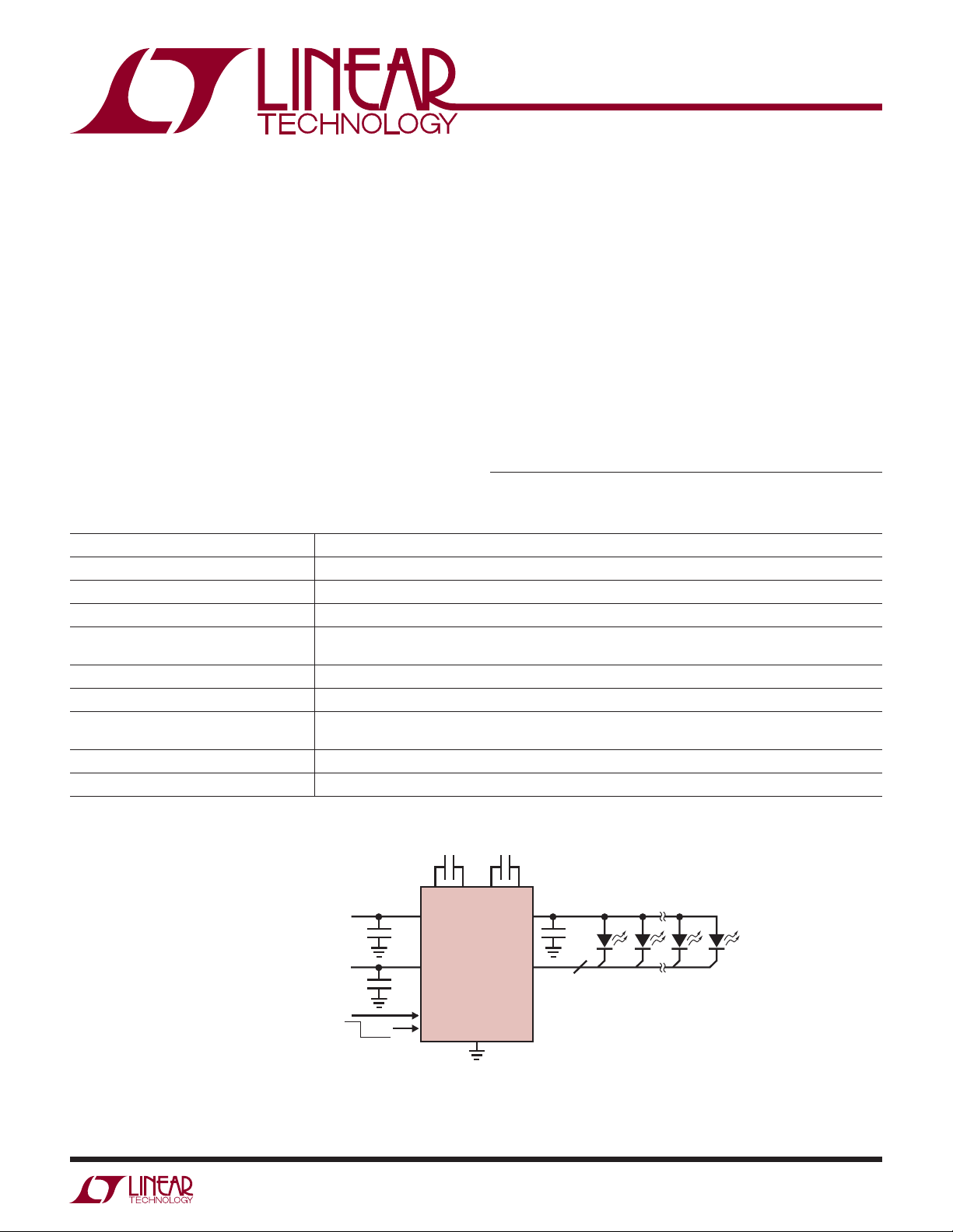
DV
C2
2.2μF
C1P C1M
V
IN
CC
I2C
RESET
C1
2.2μF
0.1μF
V
IN
DV
CC
SCL/SDA
RST
C3
2.2μF
C2P C2M
LTC3220
LTC3220-1
ULED1-18
GND
AN115 F01
Figure 1. Typical LTC3220 Application
CPO
C4
4.7μF
18
an115fa
AN115-1
Page 2
Application Note 115
Table 2. Write Word Protocol Used By the LTC3220/LTC3220-1
171181811
S Slave Address Wr A *Sub-Address A Data Byte A P**
S = Start Condition, Wr = Write Bit = 0, A = Acknowledge, P = Stop Condition
*The sub-address uses only the fi rst 5 bits, D0, D1, D2, D3 and D4.
**Stop can be delayed until all of the data registers have been written.
Table 3. Sub-Address Byte Assignment
MSB LSB
76543210Register Function
00000000 REG0 COMMAND
00000001 REG1 ULED1
00000010 REG2 ULED2
00000011 REG3 ULED3
00000100 REG4 ULED4
00000101 REG5 ULED5
00000110 REG6 ULED6
00000111 REG7 ULED7
00001000 REG8 ULED8
00001001 REG9 ULED9
00001010 REG10 ULED10
00001011 REG11 ULED11
00001100 REG12 ULED12
00001101 REG13 ULED13
00001110 REG14 ULED14
00001111 REG15 ULED15
00010000 REG16 ULED16
00010001 REG17 ULED17
00010010 REG18 ULED18
00010011 REG19GRAD/ BLINK
I2C Control
The LTC3220/LTC3220-1 has 20 data registers, each with
its own sub-address as shown in Table 3. The data is
loaded into the registers when the device receives a Stop
2
bit. This device is written using the standard I
C protocol
(a 7-bit slave address and write bit, followed by the 8-bit
sub-address byte and an 8-bit data byte) as illustrated
2
in Table 2. This device is a slave I
C device that can only
receive data.
The only difference between the LTC3220 and the
2
LTC3220-1 is the 7-bit I
address is 0011100 and the LTC3220-1 I
C address. The LTC3220 I2C
2
C address is
0011101.
AN115-2
DATA BYTES
Register 0 (Table 4 and Table 5) is used to enter or exit
shutdown, set the charge pump to Auto, Force 1x, Force
1.5x, or Force 2x modes, and to parallel write to the part
using the Quick Write bit. Register 1 through register 18 set
the intensity and mode for each of the eighteen individual
ULED outputs (Table 6). Register 19 is separated into three
portions as illustrated in Table 7, Table 8 and Table 9. The
blink bits, D4 and D3, are used to select the blinking ontime and period. The gradation timer bits, D2 and D1, are
used to control the gradation time while the Up bit, D0, is
used to control the gradation ramp direction.
an115fa
Page 3
Application Note 115
Table 4. REG0, Command Byte
MSB LSB
D7 D6 D5 D4 D3 D2 D1 D0
Unused Unused Unused Unused Shutdown Force2x Force1p5x Quick Write
Table 5. Command Byte Bit Functions
Quick Write 01Serial Write to Each Register
Force1p5x 10Forces Charge Pump into 1.5x Mode
Force2x 10Forces Charge Pump into 2x Mode
Force1x D1 (Force1p5x) =1
Shutdown 10Shuts Down Part, While Preserving Data in Registers
Table 6. REG1 to REG18, Universal LED 6-Bit Linear DAC Data with Blink/Gradation/GPO Modes
BLINK/GRADATION/GPO MODE BITS LED CURRENT DATA
Normal
Blink Enabled
Gradation Enabled
GPO Mode*
Strong Pull-Down Mode
Current Limited Mode
High Impedance/OFF
*(Gradation/Blink/Dropout Disabled)
Parallel Write, REG1 Data Is Written to All Eighteen Universal Registers
Enables Mode Logic to Control Mode Changes Based on Dropout Signal
Enables Mode Logic to Control Mode Changes Based on Dropout Signal
Forces Charge Pump into 1x Mode
D2 (Force2x) = 1
Normal Operation
MSB LSB
Bit 7 Bit 6 Bit 5 Bit 4 Bit 3 Bit 2 Bit 1 Bit 0
}
0
0
1
1
1
0
0
1
0
1
1
0
D5
D5
D5
0
D5
0
D4
D4
D4
0
D4
0
D3
D3
D3
0
D3
0
D2
D2
D2
D2
D1
D1
D1
0
0
0
D1
0
D0
D0
D0
0
D0
0
an115fa
AN115-3
Page 4
Application Note 115
Table 7. REG19, Gradation and Blinking Register
MSB LSB
D7 D6 D5 D4 D3 D2 D1 D0
Unused Unused Unused GB4 GB3 GB2 GB1 UP
Table 8. Gradation Up Bit
UP 01Gradation Counts Down
Table 9. Gradation and Blinking Register Bit Functions
D4 D3 Blink Period D2 D1 Times Period
0
0
1
1
Gradation Counts Up
BLINK TIMES AND PERIOD GRADATION TIMES AND PERIOD
0
1
0
1
0.625s
0.156s
0.625s
0.156s
1.25s
1.25s
2.5s
2.5s
0
0
1
1
0
1
0
1
Disabled
0.24s
0.48s
0.96s
Disabled
0.313
0.625
1.25
AN115-4
an115fa
Page 5

Application Note 115
DEVICE SETUP AND OPERATION
This device requires an input supply of 2.9V to 5.5V and
a DV
supply of 1.5V to 5.5V. Refer to the LTC3220/
CC
LTC3220-1 data sheet for electrical connections and
specifi cations. Although the power on reset clears all the
data registers, it is good practice to reset the part using the
RST pin to make sure all data registers are reset after V
and/or DV
be used to clear all ULED registers with few I
power up. The Quick Write feature may also
CC
2
C writes.
IN
SET ONE OR MORE ULED OUTPUT(S)
2
To set one or more ULED output(s) using the I
C bus,
write the intensity setting to the desired ULED registers
with the mode enable bits (Bit 7 and Bit 6) low, followed
by a Stop bit. The following example illustrates how to set
ULED1 and ULED2 to 5mA. Since the full-scale current is
20mA, use the following formula to determine the number
of steps needed to acquire 5mA.
Steps = ILED • StepsFullScale/IFullScale (1)
5mA • 63Steps/20mA = 15.75 Steps
The number of steps is rounded to 16 and converted to
the hexadecimal value 10H. Setting the ULED register to
10H will set the ULED output to approximately 5mA. In
Example 1, the “S” designates the Start Bit and 38H des-
2
ignates the LTC3220 7-bit I
C address plus the write bit to
form the 8-bit hexadecimal byte of 38. For the LTC3220-1,
2
substitute 3AH in place of 38H for the I
C address. The
second hexadecimal bytes, 01 and 02, are the sub-address
bytes. The third hexadecimal byte is the register data byte.
The “P” designates the Stop bit. The Stop bit was set after
the last write to load ULED1 and ULED2 registers and set
the ULED outputs simultaneously. A Stop bit may be used
2
after each I
C write, however it is not desired in some
cases while gradating. All of the following examples will
use the same format used in Example 1.
Example 1. Setting ULED1 and ULED2 to 5mA.
S 38H 01H 10H* ‘Set ULED1 to 5mA, No Stop bit
needed
S 38H 02H 10H P ‘Set ULED2 to 5mA, Stop bit
loads data
*A Stop bit may be used here if desired.
USING THE GPO FEATURE
This device has two GPO modes: the Current Limited GPO
mode limits the output current from 0.4mA to 20mA in
63 steps and the Strong Pull-Down GPO mode acts like
a switch. The GPO modes may be used as an open drain
output to drive a logic signal to a microprocessor or some
other device. This is accomplished by allowing the ULED
pin to be driven to 0V without causing the charge pump
to change modes.
If the device is forced into shutdown while in Current
Limited GPO mode, the output is disabled and the supply current will be reduced to a few hundred microamps.
This mode is useful for driving other devices which are
not to be controlled during shutdown, or to control the
current to other devices which would otherwise cause the
LTC3220/LTC3220-1 to go into dropout. When a Current
Limited GPO is used as an open drain output, the current
setting should be set greater than the maximum current
needed. However a current setting greater than 10 times
the maximum current may increase the quiescent current
by more than 10%.
To set one or more ULED output(s) to Current Limit GPO
mode, write the intensity setting greater than 0mA to
the desired ULED registers with the GPO mode enable
bits (Bit 7 and Bit 6) high, followed by a Stop bit. It was
determined using formula (1) that 3 steps are required to
provide 1mA, therefore the hexadecimal code needed to
provide 1mA of current in GPO mode is C3H. Example 2
illustrates how to set ULED1 and ULED2 to 1mA Current
Limited GPO mode.
an115fa
AN115-5
Page 6

Application Note 115
Example 2. Set ULED1 and ULED2 to 1mA in Current
Limited GPO mode.
S 38H 01H C3H* ‘Set ULED1 to 1mA in GPO mode
S 38H 02H C3H P ‘Set ULED2 to GPO mode, Stop
bit loads data
*A Stop bit may be used here if desired.
In Strong Pull-Down GPO mode, the current is not limited
by the device and needs to be limited externally to 25mA or
less. The advantage of this mode is that it only uses 3μA
of quiescent current and may be used while the part is in
shutdown. CPO should not be used for supplying current
to a Strong Pull-Down GPO during shutdown since CPO
is limited by a weak pull-up current source. To set one or
more ULED output(s) to Strong Pull-Down GPO mode,
write the intensity setting of 0mA to the desired ULED
registers with the GPO enable bits high as illustrated in
Table 6. A Stop bit loads the data and sets the output.
Example 3 illustrates how to set ULED1 and ULED2 into
Strong GPO mode.
of shutdown, the ULED outputs will start blinking in the
“off” state. To set one or more ULED output(s) blinking,
set the blinking rate in register 19, and then set the ULED
register(s) and blinking bit with the desired intensity. Send
a Stop bit to start the ULED output(s) blinking. The blink
rate may be changed at any time by changing the blink
bits in register 19. Example 4 shows how to start ULED1
and ULED2 blinking.
Example 4. Setting ULED1 and ULED2 to blink at 5mA
with a 2.5s period and a 0.625s on-time.
S 38H 13H 10H* ‘Set blinking time to 0.625s on,
2.5s period
S 38H 01H 50H* ‘Set ULED1 to blink at 5mA
S 38H 02H 50H P ‘Set ULED2 to blink, Stop bit
loads all data
*A Stop bit may be used here if desired.
USING GRADATION
Example 3. Set ULED1 and ULED2 to Strong GPO
mode.
S 38H 01H C0H* ‘Set ULED1 to Strong GPO mode
S 38H 02H C0H P ‘Set ULED2 to Strong GPO mode,
Stop bit loads data
*A Stop bit may be used here if desired.
USING THE BLINKING FEATURE
Blinking LEDs may be used to indicate voicemail messages, missed calls, low battery, or other messages. The
LTC3220/LTC3220-1 has a blinking feature that allows the
user to choose between one of four different blinking rates
as illustrated in Table 9. This feature reduces processor
2
time and I
C traffi c. The blinking times are controlled by
a single free running counter. When one or more ULED
outputs are set to blink, they will synchronously blink with
the blinking timer. The ULED outputs may start blinking in
the “on” or the “off” state except when the part is coming out of shutdown. When the device starts blinking out
It is sometimes desirable to gradually turn on and off LEDs
2
or displays. Normally substantial I
C bus time is required
to gradually turn on and off LEDs. The LTC3220/LTC3220-1
has a gradation feature that allows the user to smoothly
2
turn on and off LEDs with little I
C interaction. This device
uses a single gradation ramp to gradate one or more
LED(s) from off-to-on or from on-to-off simultaneously.
Ideally the ULED gradation enable bit and the gradation
timer are enabled at the same time as described in the
following procedures. If the gradation mode bit is set in
the ULED register prior to starting the gradation timer,
the ULED outputs will provide a 100μA current which will
cause the LEDs to turn on.
Gradation consists of a gradation time and a gradation
period. The gradation period is the time that the gradation
timer is running. The gradation timer starts running as
soon as the gradation timer bits are loaded into register
19 and stops after a set amount of time. The gradation
time is when the LED current starts to change to when it
stops changing. This typically starts 40ms after the gradation timer has started and is approximately 80% of the
AN115-6
an115fa
Page 7

Application Note 115
gradation period. The gradation period can be observed
on the down gradation ramp as shown in Figure 2. The
gradation period shown in Figure 2 is 670ms and the
gradation time is about 570ms.
I
LED
5mA/DIV
SCL
SDA
START OF
GRADATION
PERIOD
END OF
GRADATION
PERIOD
100ms/DIV
Figure 2. 625ms Gradation Period
AN115 F02
GRADATING ONE OR MORE ULED OUTPUT(s) UP
FROM OFF-TO-ON
To gradate one or more ULED output(s) from the off-to-on
2
state via the I
C bus, the gradation timer bits in register
19 (D2 and D1) should be initialized to 0. Set the ULED
register to the desired intensity with the gradation bit (Bit 7)
set without sending a Stop bit. Then set the gradation time
and the gradation Up bit (D0) high in register 19. The Stop
bit loads the registers and starts the gradation process.
Example 5 illustrates how to gradate ULED1 and ULED2
from 0mA to 5mA. Figure 3 illustrates how a ULED output
current is ramped from 0mA to 5mA at 0.48s.
Example 5. Gradating ULED1 and ULED2 from 0mA to
5mA at 0.48s:
S 38H 13H 00H P ‘Clear gradation timer if not
already clear
S 38H 01H 90H** ‘Set ULED1 to gradate to 5mA
S 38H 02H 90H** ‘Set ULED2 to gradate to 5mA
Prior to disabling the gradation timer or gradating up any
other ULED outputs, the gradation bits in the ULED register must be cleared
. This is accomplished by writing an
intensity value with the gradation bit cleared as illustrated
in Example 6
Example 6. Disabling gradation with ULED1 and
ULED2 at 5mA.
S 38H 01H 10H* ‘Set ULED1 to 5mA with
gradation bit low
S 38H 02H 10H* ‘Set ULED2 to 5mA with
gradation bit low
S 38H 13H 00H P ‘Disable gradation, Stop bit loads
all data
*A Stop bit may be used here if desired.
GRADATING ONE OR MORE ULED OUTPUT(S) DOWN
FROM ON-TO-OFF
The gradating down procedure is similar to the gradating
up procedure except the initial state of the ULED output
and the state of the Up bit in register 19. One advantage
of the LTC3220/LTC3220-1 compared to its predecessors
is that the ULED registers are automatically set to 0 when
the gradation down ramp completes. This allows the ULED
outputs to turn off and the part to go into shutdown with-
2
out any additional I
ULED output(s) from the on-to-off state via the I
C interaction. To gradate one or more
2
C bus,
the gradation timer in register 19 (D2 and D1) should be
initialized to 0. Set the ULED register to the initial intensity
with the gradation bit (D7) set without sending a Stop
bit. Then set the gradation time and the gradation Up bit
(D0) low in register 19 followed by a Stop bit as shown
in Example 7. The Stop bit loads the registers and starts
the gradation process. Figure 4 illustrates how the ULED
current gradates down from 5mA to 0mA in 0.48s.
S 38H 13H 05H P ‘Set gradation time to 0.48s and
set the Up Bit, Stop bit starts
gradation
**A Stop bit may be used here but is not desired
an115fa
AN115-7
Page 8

Application Note 115
SDA
2V/DIV
SCL
2V/DIV
I
LED
1mA/DIV
100ms/DIV
Figure 3. Gradation from 0mA to 5mA in 0.48s
SDA
2V/DIV
SCL
2V/DIV
I
LED
1mA/DIV
100ms/DIV
Figure 4. Gradation from 5mA to 0mA in 0.48s
AN115 F03
AN115 F04
USING QUICK WRITE
The Quick Write feature allows the user to control all 18
2
ULED outputs simultaneously with few I
C commands by
parallel writing the 18 ULED registers. This feature may be
used to set, clear, blink, gradate, or set the ULED outputs
into GPO mode. To set (or clear) all ULED outputs using
the Quick Write feature, fi rst set the Quick Write bit in the
Command register. Then set the ULED1 register to the
desired value. When done using the Quick Write feature,
clear the Quick Write bit. Example 8 illustrates how to clear
all of the ULED registers using the Quick Write feature.
Example 8. Clear all ULED registers using the Quick
Write Feature.
S 38H 00H 01H* ‘Set the Quick Write Bit
S 38H 01H 00H P ‘Load the ULED1 Register
with 00H
S 38H 00H 00H P*** ‘Clear Quick Write Bit, Stop bit
Sets all Registers to 0
*A Stop bit may be used here if desired.
Example 7. Gradating ULED1 and ULED2 from 5mA
to 0mA at 0.48s (ULED1 and ULED2 previously set to
10H, 5mA).
S 38H 13H 00H P ‘Clear gradation timer if not
already clear
S 38H 01H 90H** ‘Set ULED1 with gradation bits
S 38H 02H 90H** ‘Set ULED2 with gradation bits
S 38H 13H 04H P ‘Set gradation timer with Up bit
low and start gradation
**A Stop bit may be used here but is not desired
See Appendix A for more information on gradation and
gradation programming techniques.
***This step is only need if the Quick Write feature is no
longer needed.
All ULED outputs may be set to blink or GPO mode using
the Quick Write feature by setting the mode enable bits
when loading the ULED1 register as shown in Example
8. However, the desired blinking time should be selected
prior to enabling all ULED outputs in blink mode.
AN115-8
an115fa
Page 9

Application Note 115
USING PROGRAMABLE SHUTDOWN
The programmable shutdown allows the user to shutdown
the device at anytime while maintaining the data in all of
the data registers. During shutdown, all ULED outputs
not in Strong GPO mode will turn off, CPO will connect
via a weak switch, and the LTC3220/LTC3220-1 will
to V
IN
only consume about 3uA. When the device comes out of
shutdown, all ULED outputs and the charge pump will
return to their pre-shutdown state. If the ULED output
was set to blink, it will start blinking starting with the off
cycle at the previously selected on-time and period. If a
ULED output was set to gradate up, it will gradate up at
the previously selected gradation time. If shutdown was
programmed after a ULED output has completed a gradation down cycle, the output will remain off when shutdown
ends. If shutdown was programmed while a ULED output
was gradating down, the gradation ramp will reset and the
ULED output will go to the previous set intensity and then
SDA
2V/DIV
SCL
2V/DIV
START
SHUTDOWN
gradate down at the set gradation time. Figure 5 shows
how a gradation down cycle is reset if shutdown is set
before the gradation cycle completes.
CONCLUSION
The LTC3220/LTC3220-1 features are designed to give the
user more control of LEDs or other devices while minimizing
2
C bus time and battery power. The blinking and gradation
I
features allow the user to provide visual effects without
2
extensively using the I
C bus. The Strong GPO mode allows the user to control other devices while using only
3μA of quiescent current when the part is in shutdown.
The Quick Write feature allows all of the outputs to be
2
changed at once with little I
C interaction. The shutdown
feature puts the device into shutdown and will return the
device to its pre-shutdown state. All these features make
controlling complex illumination schemes easier.
STOP
SHUTDOWN
RESTART
GRADATION
CYCLE
ULED
I
LED
1mA/DIV
Figure 5. Shutdown Set During a Gradation Down Cycle
OFF
50ms/DIV
AN115 F05
an115fa
AN115-9
Page 10

Application Note 115
APPENDIX A: MORE GRADATION TECHNIQUES
CONTINUOUSLY GRADATING ONE OR MORE ULED
OUTPUT(S) UP AND DOWN
It may be desired to continuously gradate a ULED output
up and down. This may be achieved by fi rst initiating the
gradation as in Example 5 or Example 7. To gradate down
again after gradating up, clear the Up bit in register 19.
Do not clear the gradation timer bits in register 19 or the
gradation enable bit in the ULED register. If it is desired
to change the gradation ramp time, the gradation timer
bits may be changed when clearing the Up bit in register
19. Example 9 illustrates how to gradate back down again
without resetting the gradation enable bit or gradation
timer bits.
Example 9. Gradating down after gradating up as
illustrated in Example 5.
S 38H 13H 04H P ‘Clear Up bit, Stop bit starts
gradation ramp down
To gradate back up after gradating down is similar to gradating one or more ULED outputs up. The only difference
is that the gradation timer does not have to be reset as in
Example 5. Gradating back up is done by setting the ULED
intensity and the gradation bit without a Stop bit. Then set
the gradation Up bit and gradation timer in register 19,
as illustrated in Example 10. If a different gradation rate
is desired, the gradation time may be changed when the
Up bit is set in register 19.
Example 10. Gradating ULED1 and ULED2 back up to
5mA after gradating down.
CONTINUOUSLY GRADATING ONE OR MORE ULED
OUTPUT(S) UP AND DOWN WITH STOP BITS AFTER
2
EVERY I
C WRITE
If a Stop bit must be set after the ULED registers are written when gradating up and prior to setting the gradation
timer and Up bit, one of two results will occur. If the device
went into shutdown after gradating down, then the ULED
output(s) will jump to the destination gradation current
after the ULED register data and Stop bit are received. The
ULED will remain at this setting until the gradation timer
is set. This may cause an LED to fl ash briefl y. Figure 6
illustrates how a ULED output current jumps after loading
the ULED register until the gradation timer is set with a
clock speed of 100KHz. This fl ash may be reduced to tens
2
of microseconds by using a 400KHz I
C clock and reducing
the delay between bytes and start and stop bits.
SDA
2V/DIV
SCL
2V/DIV
1ST STOP BIT
I
LED
1mA/DIV
200μs/DIV
Figure 6. Gradating Up After Gradating Down and Going Into
Shutdown. Stop Bit After 1st Stop Bit Causes ULED Output to
Jump Until Gradation Timer Is Set with 2nd Stop Bit
2ND STOP BIT
START
GRADATION
CYCLE
AN115 F06
S 38H 01H 90H** ‘Set ULED1 to gradate to 5mA
S 38H 02H 90H** ‘Set ULED2 to gradate to 5mA
S 38H 13H 05H P ‘Set Up bit, Stop bit starts
gradation
**A Stop bit may be used here but is not desired
AN115-10
an115fa
Page 11

Application Note 115
When a part is not in shutdown after the gradating down
and the ULED register data and a Stop bit were received,
the ULED output will provide a 100μA current until the
gradation timer is loaded. This 100μA output state may
2
be reduced by using a 400KHz I
C clock and reducing the
delay between bytes, Start, and Stop bits. Figure 7 illustrates how a ULED output provides 100μA after loading
the ULED register until the gradation timer is set with a
clock speed of 100kHz.
SDA
2V/DIV
SCL
2V/DIV
200μs/DIV
2ND START BIT
STARTS GRADATION
AN115 F07
1ST STOP BIT
I
LED
500μA/DIV
Figure 7. Gradating Up After Gradating Down and Device Does
Not Go into Shutdown
ULED STARTS AT 100μA
GRADATING MULTIPLE ULED OUTPUTS IN SAME
DIRECTION CONSECUTIVELY
It may be desired to gradate a number of ULED outputs
in the same direction consecutively. This is easily done,
however since there is only one gradation ramp one gradation cycle must be completed prior to starting the next.
To gradate multiple ULED outputs up consecutively, fi rst
initiate gradation as done in Example 5. After the gradation cycle has completed, disable gradation as done in
Example 6, then start the next ULED output gradating as
done in Example 5.
Gradating down consecutive ULED outputs is even less
complicated since the ULED registers are cleared automatically after the gradation cycle has completed. To do this,
gradate the fi rst ULED output down as illustrated in Example
7. Wait until the gradation down cycle has completed and
then clear the gradation timer. Now gradate the next ULED
down again as shown in Example 7.
GRADATING USING QUICK WRITE
The Quick Write feature may also be used to gradate up or
down. This process is similar to setting the ULED outputs
in normal mode using the Quick Write feature except the
gradation time is set prior to sending a Stop bit. The ULED
outputs may also be gradated up and down consecutively
by leaving the Quick Write bit set, changing the Up bit in
register 19, and reloading the ULED1 register prior to the
up gradation. Example 11 illustrates how to consecutively
gradate all ULED outputs up and down using the Quick
Write feature.
Information furnished by Linear Technology Corporation is believed to be accurate and reliable.
However, no responsibility is assumed for its use. Linear Technology Corporation makes no representation that the interconnection of its circuits as described herein will not infringe on existing patent rights.
an115fa
AN115-11
Page 12

Application Note 115
Example 11. Gradate all ULEDs Up and Down using
the Quick Write Feature.
S 38H 00H 01H* ‘Set the Quick Write Bit
S 38H 01H 90H** ‘Load the ULED1 Register
with 90H
S 38H 13H 05H P ‘Set the Gradation Timer and
Up Bit, Stop Bit starts gradation
Wait for gradation period to fi nish.
S 38H 13H 04H P ‘Clear the gradation Up Bit,
Stop Bit starts gradation
Wait for gradation period to fi nish.
S 38H 01H 90H** ‘Load the ULED1 Register
with 90H
S 38H 13H 05H P ‘Set the Gradation Timer and
Up Bit, Stop Bit starts gradation
S 38H 00H 00H P*** ‘Clear Quick Write Bit
*A Stop bit may be used here if desired.
**A Stop bit may be used here but is not desired
***This step is only need if the Quick Write feature is no
longer needed.
SDA
2V/DIV
SCL
2V/DIV
1ST STOP BIT
ULED STARTS AT 100μA
I
LED
500μA/DIV
Figure 8. Start of Up Gradation when a Stop Bit Is Received
After the ULED Register Data Is Received
2ND START BIT
STARTS GRADATION
500μs/DIV
AN115 F08
If it is not possible to delay the Stop bit until after the data
is loaded when gradating down, set the ULED registers
with a Stop bit and then set the gradation timer and clear
the Up bit in register 19 with as little delay as possible
between writes. Although the ULED outputs will provide
100μA within tens of microseconds of the corresponding
Stop bit, all of the ULED outputs will return to their initial
state and gradate down together after the gradation timer
is loaded. Figure 9 illustrates how the ULED output current
will behave when a Stop bit is sent after the ULED register
is written to using a 100kHz clock speed with a 400μs
delay between writes. This 100μA state may be reduced by
using a 400kHz clock and by reducing the delay between
bytes and start and stop bits.
2
GRADATING WITH STOP BITS AFTER EVERY I
C WRITE
If it is not possible to delay the Stop bit until after the data
is loaded when gradating up, set the ULED registers with
a Stop bit and then set the gradation timer and Up bit in
register 19 with as little delay as possible between writes.
Although the ULED outputs will turn on at 100μA within
several hundreds of microseconds, all of the ULED outputs
will gradate together after the gradation timer is loaded.
Figure 8 shows the ULED output current at 100μA until
the gradation timer is set in register 19 using a 100kHz
2
C clock. The duration of this 100μA current state may
I
be reduced by using a 400kHz I2C clock and reducing the
delay between bytes and start and stop bits.
Linear Technology Corporation
AN115-12
1630 McCarthy Blvd., Milpitas, CA 95035-7417
(408) 432-1900 ● FAX: (408) 434-0507
●
www.linear.com
SDA
2V/DIV
SCL
2V/DIV
I
LED
1mA/DIV
1ST STOP BIT
100μA
STAT E
200μs/DIV
Figure 9. Start of Gradation from 5mA to 0mA with A Stop Bit
After Writing the ULED Register
© LINEAR TECHNOLOGY CORPORATION 2008
2ND STOP BIT
START
GRADATION
AN115 F09
LT 0308 REV A • PRINTED IN USA
an115fa
 Loading...