

Page 1
Application Note 10
Methods of Measuring Op Amp Settling Time
Jim Williams
July 1985
Servo, DAC and data acquisition amplifiers all require
good dynamic response. In particular, the time required
for an amplifier to settle to final value after an input step
is especially important. This specification allows setting
a circuit’s timing margins with confidence that the data
produced is accurate. The settling time is the total length
of time from input step application until the amplifier remains within a specified error band around the final value.
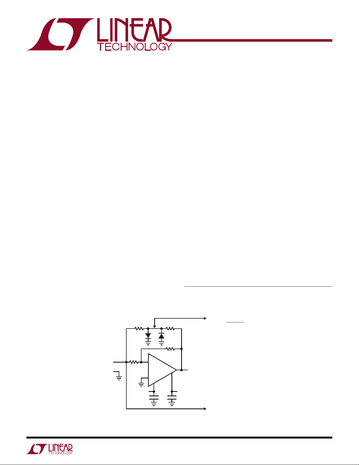
Figure 1 shows one way to measure amplifier settling
time (see References 1, 2, and 3). The circuit uses the
“false sum node” technique. The resistors and amplifier
form a bridge-type network. Assuming ideal resistors, the
amplifier output will step to –V
when an input pulse is
IN
applied. During slew, the oscilloscope probe is bounded
by the diodes, limiting voltage excursion. When settling
occurs, the oscilloscope probe voltage should be zero. Note
that the resistor divider’s attenuation means the probe’s
output will be one-half of the actual settled voltage.
In theory, this circuit allows settling to be observed to
small amplitudes. In practice, it cannot be relied upon to
produce useful measurements. Several flaws exist. The
circuit requires the input pulse to have a flat top within
the required measurement limits. Typically, settling within
10mV or less for a 10V step is of interest. No generalpurpose pulse generator is meant to hold output amplitude
and noise within these limits. Generator output-caused
aberration appearing at the oscilloscope probe will be
indistinguishable from amplifier output movement, producing unreliable results. The oscilloscope connection
presents additional problems. As probe capacitance rises,
AC loading of the resistor junction will influence observed
settling waveforms. The 20pF probe shown alleviates this
problem but its 10X attenuation sacrifices oscilloscope
gain. 1X probes are not suitable because of their excessive
input capacitance. An active 1X FET probe will work, but
another issue remains.
The clamp diodes at the probe point are intended to reduce
swing during amplifier slewing, preventing excessive oscilloscope overdrive. Unfortunately, oscilloscope overdrive
recovery characteristics vary widely among different types
and are not usually specified. The diodes’ 600mV drop
means the oscilloscope may see an unacceptable overload,
bringing displayed results into question (for a discussion of
oscilloscope overdrive considerations, see Box SectionA,
“Evaluating Oscilloscope Overload Response”).
L, LT, LTC, LTM, Linear Technology and the Linear logo are registered trademarks of Linear
Technology Corporation. All other trademarks are the property of their respective owners.
SCOPE PROBE 20pF OR LESS
4.99k4.99k
1N4148
V
IN
4.99k
–15V 15V
Figure 1. Typical Settling Time Test Circuit
1N4148
4.99k
–
AUT
+
0.01
V
0.01
SCOPE VERTICAL 1mV/DIV
V
ERROR
OUT
SCOPE VERTICAL
INPUT REFERENCE
AN10 F01
=
VIN – V
OUT
2
an10f
AN10-1
Page 2
Application Note 10
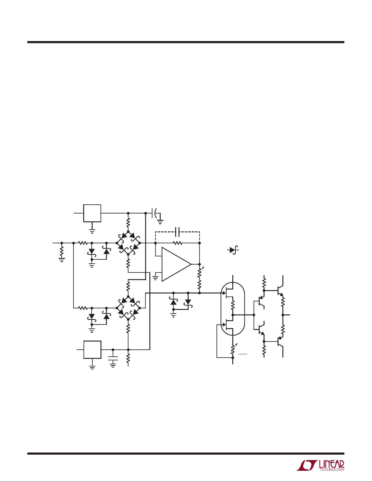
Figure 2 shows a practical settling time test circuit that addresses the problems discussed. Combined with a careful
evaluation of the test oscilloscope used, it permits reliable
settling time measurements in the 0.1% to 0.01% region.
The input pulse does not drive the amplifier, but switches
a Schottky bridge via a clamp. The bridge is biased from
two low noise LT1021-10V references. Depending on input
pulse polarity, current flows through the appropriate 10k
resistor to bias the amplifier’s summing point. The bridge
switches cleanly and quickly, producing a flat-topped
current pulse into the AUT. The circuit’s input pulse characteristics do not influence the measurement. A second
clamp-bridge arrangement supplies an opposite polarity
signal which is nulled against the amplifier’s output at
point B. Schottky clamp diodes limit this point’s voltage
excursion to ±300mV.
TTL
INPUT
PULSE
15V
50Ω
LT1021-10
IN
2k
GND
OUT
10k
1µF
+
C
(SELECT)
f
10k
A
–
The Q1-Q5 configuration forms a low input capacitance,
high speed buffer to drive the oscilloscope. Q1A’s 1pF
to 2pF input capacitance provides very light AC loading,
eliminating probe-caused problems. Q1B, running as a
current sink, compensates Q1A’s V
drop. Q2-Q5 form
GS
a complementary emitter-follower, which can drive substantial cable capacitance without distortion.
The circuit should be built on a ground planed board with
particular care taken to ensure low stray capacitance at
points A and B. The AUT socket should be selected for short
pin lengths. Very high speed amplifiers (t
SETTLE
< 200ns)
should be directly soldered into the circuit.
USE GROUND PLANE
BYPASS SUPPLIES AT
AMPLIFIER UNDER TEST
AND OUTPUT STAGE.
MINIMIMZE STRAY
CAPACITANCE AT POINTS
A AND B
ALL HP5082-2810
NC
2k
LT1021-10
OUT
GND
10k
10k
10k
2k1µF
–15V
AUT
+
B
1k
NULL TRIM
9.76k
Figure 2. Improved Settling Time Test Circuit
Q1A
Q1B
–15V
1/2 U440
50Ω
1/2 U440
100Ω
ZERO
15V15V
–15V
15V
–15V –15V
15V
4.7k
Q2
2N5160
Q3
2N3866
4.7k
Q4
2N3866
3Ω
SETTLE
OUTPUT
(TO OSCILLOSCOPE)
3Ω
Q5
2N5160
AN10 F02
AN10-2
an10f
Page 3
Application Note 10
This circuit, combined with a judiciously chosen oscilloscope, allows observation of amplifier settling to a millivolt
(0.01%) for a 10V step. A good way to gain confidence
in the circuit is to test a very fast UHF amplifier. Figure 3
shows response for an amplifier (Teledyne Philbrick 1435)
specified to settle in 70ns within a millivolt for a 10V step.
Trace A is the input pulse, Trace B is the amplifier output
and Trace C is the settle signal. Settling occurs inside
70ns, indicating good agreement between the circuit and
the AUT specification. Since most amplifiers are not nearly
this fast, it is reasonable to assume that the circuit will
always provide reliable results.
A = 5V/DIV
B = 5V/DIV
C = 5mV/DIV
Because this circuit works by nulling opposite polarity
sources, it seems unable to test followers—but it can.
The AUT is battery-powered and completely floated from
the circuit’s power supply (Figure 4). The AUT output is
connected to circuit ground and the battery center tap
becomes the output. The positive input is driven from
the Schottky bridge. The floating power supply lets the
follower fool the circuit into thinking it is testing an inverter. The AUT’s output appears inverted, but this is not
a significant penalty.
20ns/DIV
Figure 3. Settling Detail for a Fast Amplifier
+V
–
AUT
+
15V
–
+
A = –1
NULL POINT
AN10 F04
TO OUTPUT
BUFFER
+
15V
–
–V
+V
–V
Figure 4. Circuit for Testing Followers
an10f
AN10-3
Page 4

Application Note 10
To calibrate this circuit, ground point B and adjust the
“zero trim” for 0V output. Next, temporarily tie the pulse
input to +15V through 680Ω and adjust the “null trim” for
0V output. Remove the 680Ω resistor and the circuit is
ready for use. When measuring settling times remember
to experiment with the value of C
to obtain best perfor-
F
mance (see Box Section B, “Amplifier Compensation”).
In the past, amplifier settling measurements below 1mV
were not required. Recently, 16-bit and 18-bit D→A converters have become relatively common, requiring users
to consider sub-millivolt settling time performance. Also,
the offset specifications of current generation monolithic
amplifiers are good enough to make very high precision
settling time data worthwhile. Previously, being able to see
an amplifier settle within 50µV wasn’t interesting because
its thermal drift swamped this figure.
The newer amplifier’s substantially lower drift means
very high precision settling time measurement data is
useful. Figure 2’s circuit is limited to 0.01% (1mV out of
10V) resolution by the 300mV Schottky clamp potential
at point B. Simply increasing oscilloscope gain to get
higher resolution will not work because of severe overload
problems. With the oscilloscope set at 50µV/division, the
Schottky bound allows a 6000:1 overdrive. This is much
more than any vertical amplifier is designed to accommodate. The oscilloscope’s overload recovery will completely
dominate the observed waveform and all measurements
will be meaningless.
One way to obtain higher precision settling time measurements is to clip the incoming waveform in time, as well
as amplitude. If the oscilloscope is prevented from seeing
the waveform until settling is nearly complete, overload is
avoided. Doing this requires placing a switch at the settle
circuit’s output and controlling it with an input-triggered,
variable delay. FET switches are not suitable because of
their gate-source capacitance. This capacitance will allow
gate drive artifacts to corrupt the oscilloscope display,
producing confusing readings. In the worst case, gate
drive transients will be large enough to induce overload,
defeating the switch’s purpose.
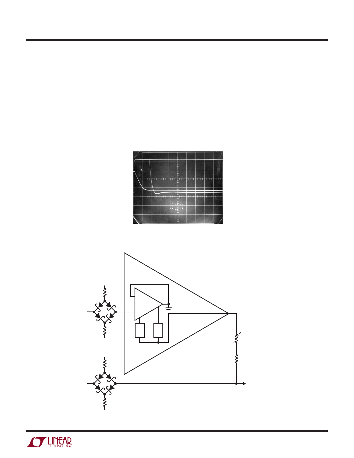
Figure 5 shows a way to implement the switch, which
largely eliminates these problems. This circuit, connected
to the basic settle circuit of Figure 2, allows settling within
10µV to be observed. The Schottkys sampling bridge is
the actual switch. The bridge’s inherent balance, combined
with matched diodes and very high speed complementary
5V
180
1N4148
0.1
Q
QA1 C1 GND
820pF
820pF
500
SKEW
COMP
LEVEL SHIFTS
1N4148
500
SKEW
COMP
0.1
20k
DELAY
2000pF
5V
ADJUST
V
CC
6 7
74123B1TO INPUT PULSE
VARIABLE
DELAY
4304.7k
Q1
2N2907
820 820
4304.7k
Q3
2N2907
820 820
Q2
2N2369
–5V
5V
Q4
2N2369
–5V
180
*
TO
SETTLE
OUTPUT
SWITCHING
BRIDGE
ALL HP5082-2810
USE GROUND PLANE
*MATCH DIODE FORWARD DROP
750
750
4.7k
2N5160
2N3866
4.7k
OUTPUT
BUFFER
15V
2N3866
3Ω
SAMPLED
OUTPUT
TO OSCILLOSCOPE
3Ω
2N5160
AN10 F05
–15V
15V
1/2 U440
2k
–15V
50Ω
1/2 U440
100Ω
ZERO
–15V
15V
AN10-4
Figure 5. Sampling Switch for Ultra Precision Settling Time Measurement
an10f
Page 5

Application Note 10
bridge switching, yields a clean, switched output. An output
buffer stage, identical to the one used in Figure 2, unloads
the bridge and drives the oscilloscope.
The complementary bridge switching drive is supplied from
the Q1-Q2 and Q3-Q4 level shifters. Each circuit converts
the delay one-shot’s TTL output to ±5V levels. The identical stages are comprised of an emitter-switched current
source feeding a Baker-clamped common emitter output.
Feedforward capacitance to the output transistor aids
speed and overall delays are about 3ns. The level shifters
must switch simultaneously to minimize drive-induced
disturbances in the bridge’s output. The “skew compensation” trims permit very small phasing adjustments in each
level shifter, compensating skew in the 74123 one-shot’s
outputs. To trim this circuit, ground the bridge input and
pulse the 74123’s C1 input. Next, set the oscilloscope to
100µV/division and adjust the skew trims for minimum
indication on the screen. Connect the bridge input back to
the settle circuit’s output and the circuit is ready for use.
Construction of this circuit requires care. A ground plane
is mandatory and all bridge connections should be as
short and symmetrical as possible. To maintain low noise,
the bridge’s output ground return should be routed away
from high current returns such as the 74123’s ground pin.
This switch circuit, carefully constructed and used with
the basic settle circuit, provides good results. Figure 6
shows an LT1001 precision op amp as the AUT. Trace A
is the input pulse, while Trace B is the AUT output. During the AUT’s slewing period the 74123 is fired (Trace C
is Q), turning off the bridge. The bridge input appears
in TraceD. The 74123 delay is adjusted so the bridge is
switched when settling is nearly complete. Trace E is the
circuit’s final output, showing settling details at 100µV/
division. The narrow peaking at the waveform’s leading
edge is due to switching residue. Figure 7 lists measured
settling times to 50µV (0.0005% of a 10V step) for a group
of precision amplifiers.
Some poorly designed amplifiers exhibit a substantial
“thermal tail” after responding to an input step. This
phenomenon, due to die heating, can cause the output to
wander outside desired limits long after settling has apparently occurred. After checking settling at high speed it is
A = 10V/DIV
B = 10V/DIV
C = 10V/DIV
D = 1V/DIV
E = 100µV/DIV
10µs/DIV
Figure 6. Sampling Switch Waveforms
Amplifier Settling Time Remarks
LT1001 65µs
LT1007 18µs
LT1008 65µs Standard Compensation
LT1008 35µs Feedforward Compensation
LT1012 70µs
LT1055 6µs
LT1056 5µs
Figure 7. Measured Settling Times to 0.0005%
an10f
AN10-5
Page 6

Application Note 10
always a good idea to slow the oscilloscope sweep down
and look for thermal tails. Often the thermal tail’s effect can
be accentuated by loading the amplifier’s output. Figure8
100µV/DIV
10ms/DIV
Figure 8. Typical Thermal Tail
REFERENCES
Analog Devices AD544 Data Sheet, “Settling Time Test
Circuit.”
National Semiconductor, LF355/356/357 Data Sheet, “Settling Time Test Circuit.”
Precision Monolithics, Inc., OP-16 Data Sheet, “Settling
Time Test Circuit.”
shows the thermal tail of an amplifier, which appears to
have settled in a much shorter time than it actually has.
R. Demrow, “Settling Time of Operational Amplifiers,”
Analog Dialogue, volume 4-1, 1970 (Analog Devices).
R. A. Pease, “The Subtleties of Settling Time,” The New
Lightning Empiricist, June 1971, Teledyne Philbrick.
W. Travis, “Settling Time Measurement Using Delayed
Switch,” Private Communication.
BOX SECTION A
Evaluating Oscilloscope Overload Performance
Settling time measurement relies heavily on the oscilloscope used. In many cases the oscilloscope is required
to supply an accurate waveform after the display has
been driven off screen. How long must one wait after
an overload before the display can be taken seriously?
The answer to this question is quite complex. Factors
involved include the degree of overload, its duty cycle,
its magnitude in time and amplitude and other considerations. Oscilloscope response to overload varies widely
between types and markedly different behavior can be
observed in any individual instrument. For example, the
recovery time for a 100X overload at 0.005V/division
may be very different than at 0.1V/division. The recovery
characteristic may also vary with waveform shape, DC
content and repetition rate. With so many variables, it is
clear that measurements involving oscilloscope overload
must be approached with caution. Nevertheless, a simple
test can indicate when the oscilloscope is being deleteriously affected by overdrive.
The waveform to be expanded is placed on the screen at a
vertical sensitivity, which eliminates all off-screen activity.
Figure A1 shows the display. The lower right hand portion
is to be expanded. Increasing the vertical sensitivity by a
factor of two (Figure A2) drives the waveform off-screen,
but the remaining display appears reasonable. Amplitude
has doubled and waveshape is consistent with the original
display. Looking carefully, it is possible to see small amplitude information presented as a dip in the waveform at
about the third vertical division. Some small disturbances
AN10-6
an10f
Page 7

Application Note 10
are also visible. This observed expansion of the original
waveform is believable. In Figure A3, gain has been further
increased, and all the features of Figure A2 are amplified
accordingly. The basic waveshape appears clearer and
the dip and small disturbances are also easier to see. No
new waveform characteristics are observed. Figure A4
brings some unpleasant surprises. This increase in gain
causes definite distortion. The initial negative-going peak,
although larger, has a different shape. Its bottom appears
less broad than in Figure A3. Additionally, the peak’s positive recovery is shaped slightly differently. A new rippling
disturbance is visible in the center of the screen. This
1V/DIV
100ns/DIV
kind of change indicates that the oscilloscope is having
trouble. A further test can confirm that this waveform is
being influenced by overloading. In Figure A5 the gain
remains the same but the vertical position knob has been
used to reposition the display at the screen’s bottom. This
shifts the oscilloscope’s DC operating point, which, under
normal circumstances, should not affect the displayed
waveform. Instead, a marked shift in waveform amplitude
and outline occurs. Repositioning the waveform to the
screen’s top produces a differently distorted waveform
(Figure A6). It is obvious that for this particular waveform,
accurate results cannot be obtained at this gain.
0.5V/DIV
100ns/DIV
0.2V/DIV
0.1V/DIV
A1
100ns/DIV
A3
100ns/DIV
A5
A2
0.1V/DIV
100ns/DIV
A4
0.1V/DIV
100ns/DIV
A6
Figures A1-A6. The Overdrive Limit is Determined by Progressively Increasing Oscilloscope Gain
and Watching for Waveform Aberrations
Information furnished by Linear Technology Corporation is believed to be accurate and reliable.
However, no responsibility is assumed for its use. Linear Technology Corporation makes no representation that the interconnection of its circuits as described herein will not infringe on existing patent rights.
an10f
AN10-7
Page 8

Application Note 10
BOX SECTION B
Amplifier Compensation
To get the best possible settling time from any amplifier,
the feedback capacitor, C
’s purpose is to roll off amplifier gain at the frequency,
C
F
, should be carefully chosen.
F
which permits best dynamic response. The optimum value
will depend on the feedback resistor’s value and the
for C
F
characteristics of the source. One of the most common
sources is also one of the most difficult. Digital-to-analog
converters’ current outputs must often be converted to
a voltage. Although an op amp can easily do this, care is
required to obtain good dynamic performance. A fast DAC
can settle to 0.01% in 200ns but its output also includes
a parasitic capacitance term, making the amplifier’s job
more difficult. Normally, the DAC’s current output is
unloaded directly into the amplifier’s summing junction,
placing the parasitic capacitance from ground to the amplifier’s input. The capacitance introduces feedback phase
shift at high frequencies, forcing the amplifier to “hunt”
and ring about the final value before settling. Different
DACs have different values of output capacitance. CMOS
DACs have the highest output capacitance and it varies
with code. Bipolar DACs typically have 20pF to 30pF of
capacitance, stable over all codes. Because of their output capacitance, DACs furnish an instructive example in
amplifier compensation. In practice, the Schottky bridge
which feeds the AUT in the settle circuit is replaced with
the DAC to be used. Depending on DAC input coding,
it may be necessary to use inverters in the DAC input
lines to maintain circuit nulling action. FigureB1 shows
the response of an industry standard DAC-80 type and
an LT1023 op amp, which is optimized for inverting
applications. Trace A is the input, while TracesB and C
are the amplifier and settle outputs, respectively. In this
example no compensation capacitor is used and the
amplifier rings badly before settling. In B2, and 82pF unit
stops the ringing and settling time goes down to 4µs.
The overdamped response means that C
dominates the
F
capacitance at the AUT’s input and stability is assured.
If fastest response is desired, C
must be reduced. B3
F
shows critically damped behavior obtained with a 22pF
unit. The settling time of 2µs is the best obtainable for
this DAC-amplifier combination.
A = 5V/DIV
B = 5V/DIV
C = 10mV/DIV
AN10-8
A = 5V/DIV
B = 5V/DIV
C = 1V/DIV
1µs/DIV
B1
A = 5V/DIV
B = 5V/DIV
C = 10mV/DIV
2µs/DIV
B2 B3
Figures B1-B3. Effects of Different Feedback Capacitors on DAC-Op Amp Combination
1µs/DIV
Linear Technology Corporation
1630 McCarthy Blvd., Milpitas, CA 95035-7417
(408) 432-1900 ● FAX: (408) 434-0507
●
www.linear.com
LINEAR TECHNOLOGY CORPORATION 1990
an10f
IM/GP 290 2K • PRINTED IN USA
 Loading...