

Page 1
Application Note 107
July 2006
Extending the Input Voltage Range of PowerPath
Circuits for Automotive and Industrial Applications
Greg Manlove
INTRODUCTION
®
The voltage range of Linear Technology’s PowerPath
circuits can be easily extended with just a few components, thus
allowing them to meet the needs of virtually all applications.
This application note presents solutions for circuits that
must withstand large negative voltages, a reverse adapter
input for example, and circuits that must withstand large
positive inputs, such as automotive load-dump.
EXTENDING THE VOLTAGE RANGE
Any of Linear’s PowerPath controller circuits can benefi t
from an extended voltage range, even those that already
have wide operating and absolute maximum voltage
ranges. For instance, the LTC4412HV and LTC4414 will
each withstand voltages from –14V to 40V, which can be
extended further using the techniques described here.
Likewise, the LTC4412’s range of –14V to 28V can be
extended. The voltage ranges of monolithic PowerPath
solutions such as the LTC4411, which ranges from –0.3V
to 6V, can also be extended, though not as far.
There are two different approaches to extending the voltage
range of the PowerPath circuits. The fi rst addresses the
negative input voltage requirements with the addition of
a Schottky diode. This change assures that the external
P-channel pass transistor is held in the off state as the
input goes below ground. The second approach allows the
ICs to operate both above the specifi ed voltage range and
below ground. The external circuit count is still compact,
requiring only three additional components.
CIRCUIT FOR LARGE NEGATIVE INPUT VOLTAGES
POWER
SUPPLY
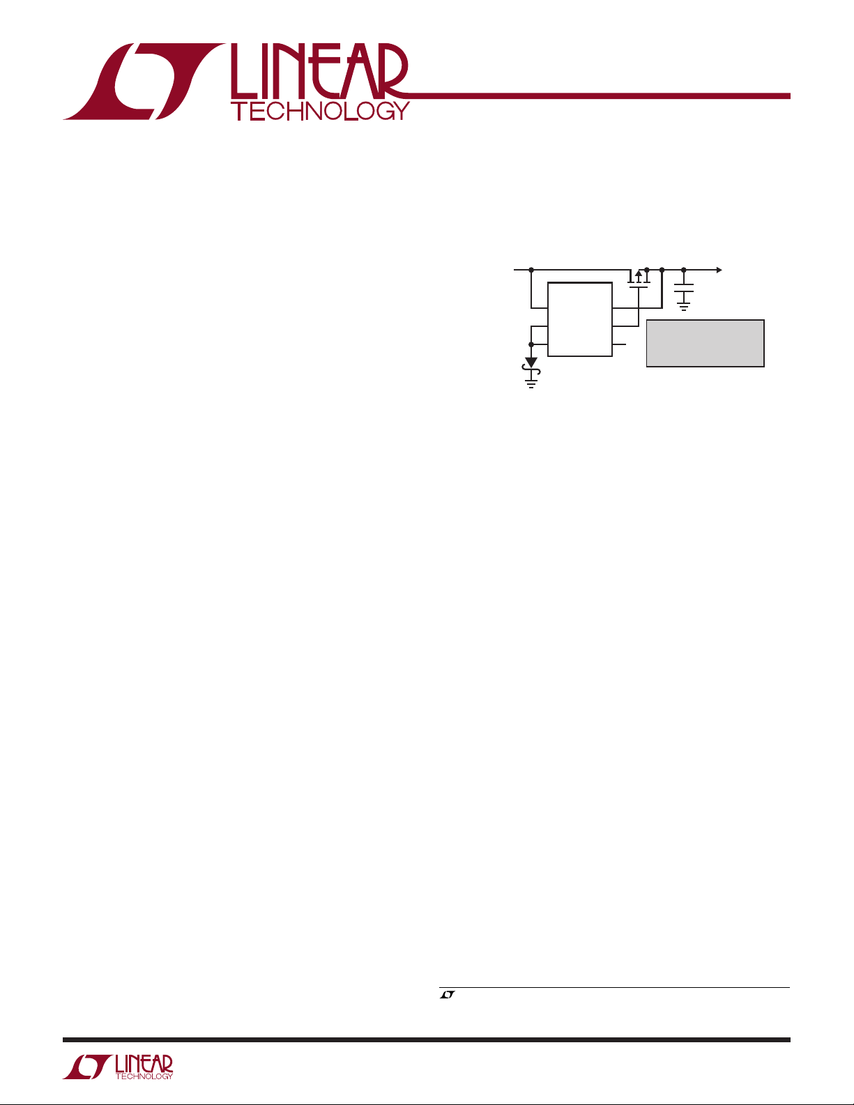
Figure 1. Circuit Capable of Operating with a Large
Negative Input Supply
PowerPath
V
SENSE
IN
GND GATE
CTL STAT
UPDATE
High voltage and floating
circuits are available
TO LOAD
C
OUT
AN 107 F01
allowed voltage difference between the Sense pin and the
pin. In the case of both the LTC4412HV and LTC4414,
V
IN
this difference is 40V, so the negative voltage limit is –40V.
Likewise, LTC4411 is limited to –6V. These values both
assume the SENSE Pin (load side) is 0V. Because the
LTC4412HV and LTC4414 are capable of withstanding –14V
with no diode present, the reverse breakdown voltage of
the Schottky diode must exceed 26V to achieve the –40V
capability at the input (40V – 14V = 26V).
During normal operation, when the input supply is positive,
the voltage at the ground pin is equal to the forward voltage
of the Schottky or approximately 0.2V. In turn, this additional
voltage on the ground pin raises the minimum operating
supply of the circuit by approximately 0.2V. The control
signal input threshold increases by the same amount.
When the input supply goes more negative than the normal
operating range of the part (–14V on the LTC4412 and
LTC4414), the ground pin begins to go negative. The IC
continues to hold the P-channel FET off as the power supply goes further below ground until the maximum V
minus V
voltage is reached (–40V on the LTC4412 and
IN
SENSE
LTC4414 and –6V on the LTC4411).
Refer to Figure 1 for a description of the circuit. The ground
and control pins of the PowerPath IC are tied through a
Schottky diode to the system ground. When the power
supply goes below ground, the diode is reverse biased,
blocking the negative supply path to ground. The maximum
negative voltage for the circuit is limited by the maximum
Information furnished by Linear Technology Corporation is believed to be accurate and reliable.
However, no responsibility is assumed for its use. Linear Technology Corporation makes no representation that the interconnection of its circuits as described herein will not infringe on existing patent rights.
The control and status pins also go negative under this large
negative supply condition. Refer to Figure 2 for a circuit that
allows control of the PowerPath IC during normal operation.
A 100k series resistor must be added between the micro-
, LT, LTC and LTM are registered trademarks of Linear Technology Corporation.
All other trademarks are the property of their respective owners.
an107f
AN107-1
Page 2
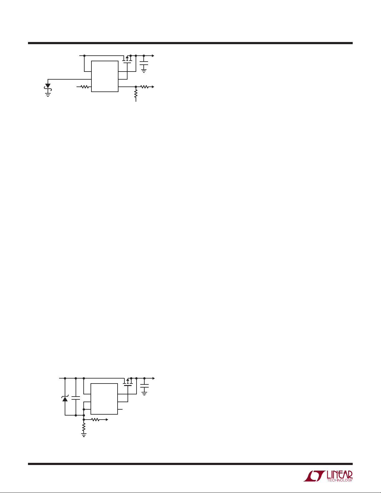
Application Note 107
POWER
SUPPLY
CONTROL
FROM MICRO
100k
PowerPath
V
SENSE
IN
GND GATE
CTL STAT
47k
V
CC
100k
C
OUT
AN 107 F02
TO LOAD
STATUS
TO MICRO
Figure 2. PowerPath Circuit Capable of Operating with a Large
Negative Supply with Control and Status Available.
processor output and the control input. The series resistor
allows the control pin to go below ground without causing
excessive current in the microprocessor or other device
controlling the part. The status pin also goes below ground
under a negative input supply, requiring a 100k resistor in
series between the status pin and the microprocessor input.
Again, the resistor is added to protect the microprocessor
from the negative input signal. Realistically, V
is not valid
CC
if the input power supply is negative, so the part operates
for all valid supply conditions. The 100k series resistors
have minimal impact on the control threshold or Status
output. Both signals have a nominal ground reference at
of the Schottky diode or approximately 0.2V. This is
the V
F
the largest deviation from nominal and should not present
a problem in most systems.
CIRCUIT FOR LARGE POSITIVE INPUT VOLTAGES
Refer to Figure 3 for a description of the circuit. The IC
ground and control pins of the PowerPath circuit are wired
together and grounded through a resistor. They are also
connected through a Zener diode to the input power supply.
The breakdown voltage on the Zener must be less than
the breakdown voltage of the IC: that is, a 5V Zener for
the LTC4411, and a 36V Zener for both the LTC4412HV
and the LTC4414.
When a large positive voltage is applied to the system, the
POWER
SUPPLY
2k
1W
PowerPath
V
SENSE
IN
GND GATE
CTL STAT
OVERVOLTAGE STATUS
100k
Figure 3. PowerPath Circuit Capable of Operating with a
Large Positive Input Supply
AN 107 F03
C
OUT
TO LOAD
Linear Technology Corporation
AN107-2
1630 McCarthy Blvd., Milpitas, CA 95035-7417
(408) 432-1900 ● FAX: (408) 434-0507
●
www.linear.com
Zener diode clamps the voltage between the V
and ground
IN
pins of the IC. The voltage on the resistor connected to
system ground rises. The quiescent current of the PowerPath products are typically under 50μA, thus a 2k resistor
causes the nominal voltage on the ground line to rise only
0.1V. This increases the minimum operating voltage by the
voltage drop across the resistor or approximately 0.1V.
The ground resistor must have a high enough power rating
2
(V
/R) for the circuit. For example, the LTC4412HV with
a 36V Zener and an 80V input, produces 44V across the
resistor. The resistor power rating is equal to (44V)
2
/2k or
approximately 1W. If 80V only occurs during a transient,
the power rating of the resistor can be reduced.
The ground pin of the PowerPath IC is positive when the
input supply exceeds the Zener clamp voltage. This ground
signal can be run through a 100k resistor to a microprocessor input to provide a control signal to the system. The
voltage on the Overvoltage Status pin can be quite large,
injecting too much current into the microprocessor input
pin. A Schottky diode can be added between the 100k resistor and system supply to clamp the signal, if required.
When the input supply is a diode voltage below ground,
the Zener diode conducts. This pulls the ground resistor
terminal to within a diode of the negative power supply.
The part sees virtually no external voltage between the
ground and input pins. The maximum negative supply is
limited by the maximum voltage difference between V
IN
and the Sense pin. On the LTC4412HV and the LTC4414,
the limit is 40V.
The LTC4411 has a negative absolute maximum voltage of
–0.3V. The forward voltage of the Zener diode may be too
large to assure minimal current in the IC under the negative
supply condition. If the current is too large, a Schottky
diode can be placed in parallel with the Zener diode. The
reverse breakdown of the Schottky must be greater than
the Zener breakdown of 5V. The forward voltage of the
Schottky is less than 0.3V assuring no excessive current
in the IC. Again, the maximum negative voltage allowed is
the maximum differential between IN and OUT or 6V.
CONCLUSION
The circuit techniques presented here extend the supply
voltage ranges of Linear Technology’s PowerPath products,
thereby extending their applicability beyond their data
sheet voltage range.
an107f
LT 1006 • PRINTED IN USA
© LINEAR TECHNOLOGY CORPORATION 2006
 Loading...