

Page 1

Application Note 7
February 1985
Some Techniques for Direct Digitization of Transducer Outputs
Jim Williams
Almost all transducers produce low level signals. Normally,
high accuracy signal conditioning amplifi ers are used to
boost these outputs to levels which can easily drive cables,
additional circuitry, or data converters. This practice raises
the signal processing range well above the error fl oor,
permitting high resolution over a wide dynamic range.
Some emerging trends in transducer-based systems are
causing the use of signal conditioning amplifi ers to be
reevaluated. While these amplifi ers will always be useful,
their utilization may not be as universal as it once was.
In particular, many industrial transducer-fed systems are
employing digital transmission of signals to eliminate
noise-induced inaccuracies in long cable runs. Additionally, the increasing digital content of systems, along with
pressures on board space and cost, make it desirable to
digitize transducer outputs as far forward in the signal chain
as possible. These trends point toward direct digitization
of transducer outputs—a diffi cult task.
Classical A/D conversion techniques emphasize high level
input ranges. This allows LSB step size to be as large
as possible, minimizing offset and noise-caused errors.
For this reason, A/D LSB size is almost always above a
millivolt, with 100μV to 200μV per LSB available in a few
10V full-scale devices. The requirements to directly A/D
convert the output of a typical strain gauge transducer are
illuminating. The transducer ’s full-scale output is 30mV,
meaning a 10-bit A/D converter must have an LSB increment of only 30μV. Performing a 10-bit conversion on a
type K thermocouple monitoring a 0°C to 60°C environment
proves even more stringent. The type K thermocouple
puts out 41.4μV/°C over the 0°C to 60°C range. The LSB
increment is found by:
60 41 4
°°
CμVC
•. /
These examples furnish extraordinarily small step sizes,
far below commercially available A/D units and seemingly
impossible to digitize without DC preamplifi cation. In fact,
both transducers’ outputs may be directly digitized to stable
10-bit resolution using circuitry specifi cally designed for
the function.
This application note details circuit techniques which
directly digitize the low level outputs of a variety of transducers. The approaches described are unique in that they
do not utilize any DC gain stage. The transducer outputs
receive no DC signal conditioning; A/D conversion is directly
performed at low level. The circuits produce a serial data
output which may be transmitted over a single wire with
the characteristic noise immunity of digital systems. By
eliminating the traditional DC gain stage, these circuits
furnish a direct, economical way to digitize low level
transducer outputs without sacrifi cing performance.
1024
242
=
μV LSB
./
an7f
AN7-1
Page 2
Application Note 7
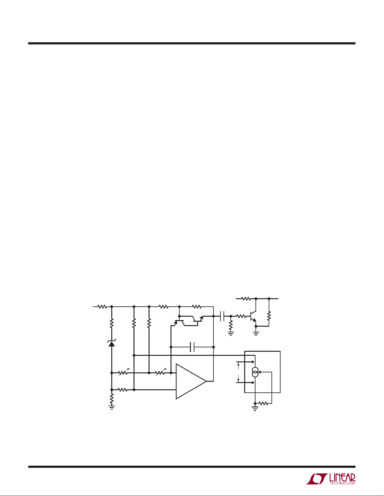
Figure 1 shows a simple way to convert the current output
of an LM334 temperature sensor to a corresponding output
frequency. The sensor pulls a temperature-dependent current (0.33%/°C) from A1’s positive input node. This point,
biased from the LM329-driven resistor string, responds
with a varying, temperature-dependent voltage. The voltage
varies the operating point of A1, confi gured as a self-resetting integrator. A1 integrates the LM329 referenced current
into its summing point, producing a negative-going ramp
at its output. When the ramp amplitude becomes large
enough, the transistors turn on, resetting the feedback
capacitor and forcing A1’s output to zero. When the capacitor’s reset current goes to zero, the transistors go off and
A1 begins to integrate negatively again. The frequency of
this oscillation action is dependent on A1’s DC operating
point, which varies with the LM334’s temperature. The
circuit’s DC biasing values are arranged so that a 0°C to
100°C sensor temperature excursion produces 0kHz to
1kHz at the output. Additionally, only 2V appear across
the LM334, minimizing sensor power dissipation related
errors. The differentiator-transistor network at A1’s output
provides a TTL compatible output. To calibrate this circuit,
place the LM334 in a 0°C environment and trim the “0°C
adjust” for 0Hz. Next, put the LM334 in a 100°C environment and set the “100°C adjust” for 1kHz output.
Repeat this procedure until both points are fi xed. This circuit
has a stable 0.1°C resolution with ±1.0°C accuracy.
Figure 2 shows another temperature-to-frequency converter, but this circuit uses the popular type K thermocouple as
a sensor. The design includes cold junction compensation
for the thermocouple over a 0°C to 60°C range. Accuracy
is ±1°C and resolution is 0.1°C.
The thermocouple’s extremely low output (41.4μV/°C) and
the requirement for cold junction compensation make it
one of the most diffi cult transducers to directly digitize.
The approach used is based on the 50nV/°C input offset
®
drift performance of the LTC
1052 chopper-stabilized
amplifi er.
In this circuit, A1’s positive input is biased by the thermocouple. A1’s output drives a crude V→F converter,
comprised of the 74C04 inverters and associated components. Each V→F output pulse causes a fi xed quantity
of charge to be dispensed into a 1μF capacitor from the
100pF capacitor via the LTC1043 switch. The larger capacitor integrates the packets of charge, producing a DC
voltage at A1’s negative input. A1’s output forces the V→F
converter to run at whatever frequency is required to balance the amplifi er’s inputs. This feedback action eliminates
drift and nonlinearities in the V→F converter as an error
560 1k* 1k*
15V
6.2k* 6.2k* 6.2k*
LM329
500Ω
0°C ADJ
820Ω*
510Ω
Figure 1. Temperature-to-Frequency Converter
2k
100°C ADJ
0.01
POLYSTYRENE
–
A1
LT1056
+
*1% FILM RESISTOR
NPN = 2N2222
PNP = 2N2907
510pF
15V
10k
2V
2.7k
10k
TTL OUT
0kHz TO 1kHz
0°C TO 100°C
4.7k
LM334-3
137Ω*
AN07 F01
an7f
AN7-2
Page 3

–
+
TYPE K
THERMOCOUPLE 41.4μV/°C
OPTIONAL INPUT
FILTER-OVERLOAD
CLAMP
50k
60°C TRIM
A
A1 LTC1052
STABILIZING AMP
1N914100k
1μF
150k**
†
COLD JUNCTION BIAS
0.1μF
33k**
1μF
301k*487Ω*
3
2
+
LTC1052
–
1
5V
–5V
7
4
16
LTC1043
8
2
6
0.1μF
3300pF
100pF
CHARGE
PUMP
65
R
T
COLD JUNCTION TEMPERATURE TRACKING
1.8k*
33k
1μF
74C04
0.68μF
74C04
4.75k*
1k*
1N4148
A
10k
5V
F
–5V
LT1004
1.2V
Application Note 7
470Ω
B
74C04C74C04D74C04E74C04
820pF
VmF
5V
3k
OUTPUT
0Hz TO 600Hz
0°C TO 60°C
187Ω*
0.01% FILM-TRW MAR-6
*
TRW/MTR/5/ + 120
**
= YELLOW SPRINGS INST. #44007
R
T
100pF = POLYSTYRENE
†
FOR GENERAL PURPOSE (1mV FULL-SCALE)
10-BIT A/D, REMOVE THERMOCOUPLE—
COLD JUNCTION NETWORK, GROUND POINT A
AND DRIVE LTC1052 POSITIVE INPUT
Figure 2. Thermocouple-to-Frequency Converter
term and the output frequency is solely a function of the
DC conditions at A1’s inputs. The 3300pF capacitor forms
a dominant response pole at A1, stabilizing the loop.
A1’s low drift eliminates offset errors in the circuit, despite
an LSB value of only 4.14μV (0.1°C)!
, a thermistor, and the 1.8k, 187Ω, 487Ω and 301k
R
T
values form a cold junction compensation network which
®
is biased from the LT
1004 1.2V reference. In addition
to cold junction compensation, the network provides
offsetting, permitting a 0°C sensor temperature to yield
0Hz at the output.
AN07 F02
Figure 3 details circuit operation. A1’s output drives the
33k-0.68μF combination, producing a ramp (Trace A,
Figure 3) across the capacitor. When the ramp crosses
inverter A’s threshold, the cascaded inverter chain switches,
producing a low output at E (Trace B). This causes the
0.68μF capacitor to discharge through the diode, resetting
the capacitor to 0V. The 820pF unit provides positive AC
feedback to inverter B’s input (Trace C), assuring a clean
reset. The frequency of this ramp-and-reset sequence varies
with A1’s output. Inverter F ’s output controls the LTC1043
switch. When the inverter output is high, Pins 2 and 6 are
connected, allowing the 100pF capacitor to charge to a
an7f
AN7-3
Page 4
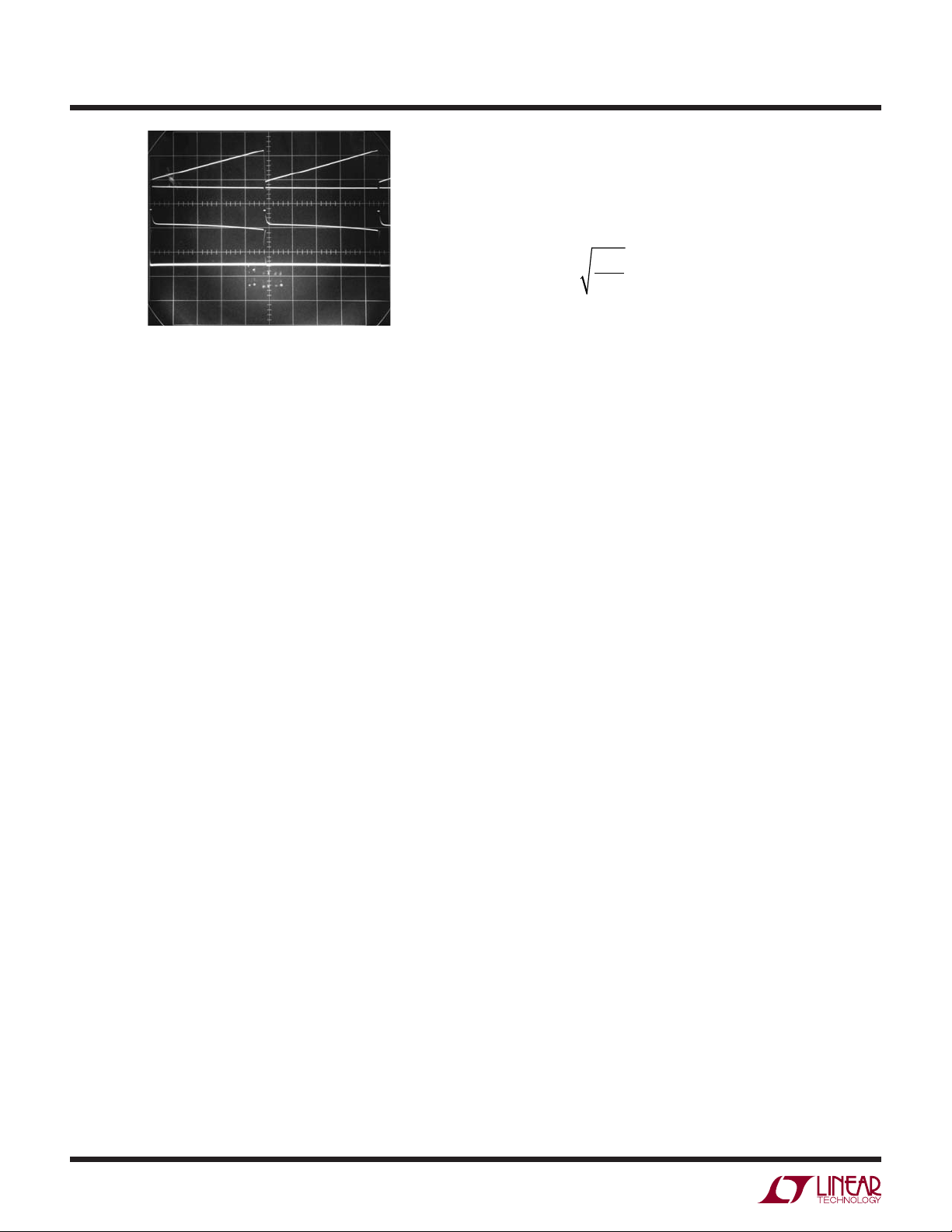
Application Note 7
A = 100mV/DIV
B = 10V/DIV
C = 10V/DIV
Figure 4 is another temperature measuring circuit, but
the transducer used is unusual. The circuit measures
temperature by utilizing the relationship between the
speed of sound and temperature in a medium. In dry air
the relationship is governed by:
D = 10μA/DIV
HORIZONTAL = 200μs/DIV
Figure 3. Thermocouple Digitizer Waveforms
AN07 F03
potential derived from the LT1004 1.2V reference. When
the inverter goes low, Pin 2 is connected to Pin 5. During
this interval, the 100pF capacitor completely discharges
(Trace D) into the 1μF unit. The amount of charge delivered
is constant over each cycle (Q = CV), so the voltage the
1μF capacitor charges to is a function of frequency and
discharge path resistance. This voltage is summed with
the LT1004-derived offsetting potential at A1’s negative
input, closing a loop around A1. The –120ppm/°C drift
of the 100pF charge-dispensing polystyrene capacitor is
compensated by the opposing tempco of the specifi ed
resistors used in the 1μF’s discharge path. Typical circuit
gain is 20ppm/°C, allowing less than 1LSB (0.1°C) output
drift over a 0°C to 70°C ambient operating range.
The thermocouple’s known characteristics, combined with
A1’s low offset and the cold junction/offsetting network
components specifi ed, eliminate zero trimming. Calibration
is accomplished by placing the thermocouple in a 60°C
environment and adjusting the 50kΩ potentiometer for
a 600Hz output. Beyond 60°C the cold junction network
departs from the thermocouple’s response and output
error increases rapidly. Although the digital output will
be a function of the thermocouple’s temperature over
hundreds of degrees, linearization by a monitoring processor is required.
It is worth noting that this circuit can directly convert any
low level, single-ended signal. If the offsetting/cold junction
network is removed and the 50kΩ potentiometer returned
directly to ground, inputs may be applied to A1’s positive
terminal. The circuit produces a 10-bit accurate output
with a full-scale range of only 1mV (1μV per LSB)! The
high impedance of A1’s input allows fi ltering or overload
clamping of the input signal without introducing error.
C = 331 5,
T
meters/second
273
where C = speed of sound.
Acoustic thermometry is used where extremes in operating temperature are encountered, such as cryogenics and
nuclear reactors. Additionally, acoustic temperature standards have been built by operating the acoustic transducer
inside a sealed, known medium.
The inherent time domain operation of acoustic thermometers allows a direct conversion into a digital output.
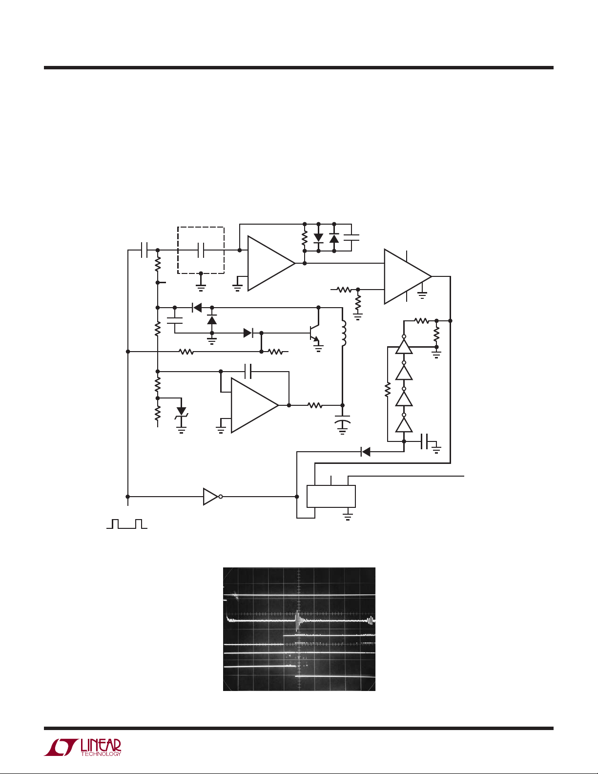
Figure 4 shows a circuit that does this. A1, the inductor,
and their associated components for a simple fl yback
type regulated 200V supply which biases the transducer.
The transducer is composed of the Polaroid ultrasonic
element noted, mounted at one end of a sealed, 6-inch
long Invar tube. The Invar material minimizes mechanical
tube deformation with temperature. The medium inside
the tube is dry air. The transducer may be thought of as a
capacitor, composed of an insulating disc with a conductive coating on each side.
Each time the TTL clock (Trace A, Figure 5) goes high,
the transducer receives AC drive via the 0.22μF capacitor.
This drive causes mechanical movement of the disc and
ultrasonic energy is emitted. The clock input simultaneously sets the 74C74 fl ip-fl op output (Trace E) low and
pulls the 0.01μF capacitor to ground. This cuts off drive
to C1’s 3k output pull-up resistor (Trace C), forcing C1’s
output (Trace D) to zero. During the clock pulse’s period,
A2’s output (Trace B) is saturated due to excessive signal
at its input. When the clock pulse ceases, A2 comes out
of bound and amplifi es in its linear region. The ultrasonic
transducer now acts like a capacitance microphone, with
the 200V supply providing bias. Residual disc ringing is
picked up and appears at A2’s output. This signal cannot
trigger C1, however, because the 0.01μF capacitor has not
charged high enough to allow the inverter to chain output
to bias C1’s output pull-up resistor.
AN7-4
an7f
Page 5
Application Note 7
The ultrasonic energy emitted by the transducer travels
down the tube, bounces off the far end and heads toward
the transducer. Before it returns, the 0.01μF capacitor
crosses the inverter’s threshold and C1’s 3k resistor
(Trace C) receives bias. Upon returning, the sonic energy
causes a mechanical displacement of the transducer, forcing a shift in capacitance. This capacitance shift causes
charge to be displaced into C2’s summing point, and the
INVAR
TUBE
0.22
600V
100M**
ENCLOSURE
TRANSDUCER
10k
200V
1N645
0.01
2k 39k
1N645
1N914
0.02
–
LT1056
+
10M
A2
–15V
output responds with an amplifi ed version of this signal
(Trace B). C1’s output (Trace D) triggers, resetting the fl ipfl op. The fl ip-fl op’s output pulse (Trace E) represents the
transit time down the tube and will vary with temperature
according to the equation given. A monitoring processor
can convert this pulse width into the desired temperature
information.
1N4148
15V
2N3440
10pF
14.7k
250Ω
L
–
+
15V
15V
C1
LT1011
–15V
7
1
3k
22k
INPUT
TTL CLOCK INPUT
100Hz, 10μs
–15V
1.2M*
10k
LT1004
2.5V
1/6 74C04
A = 20V/DIV
B = 20V/DIV
C = 20V/DIV
D = 20V/DIV
–
100Ω
15V
R Q
74C74
S
+
22
1N4148
LM307
+
A1
Figure 4. Acoustic Thermocouple
180k
L = AIE VERNITRON-24-104 1MHy
TRANSDUCER = POLAROID-604029
ENCLOSURE = INVAR 6" TUBE SEALED, DRY AIR
*
1% FILM RESISTOR
**
VICTOREEN #MOX-300
74C04
0.01
WIDTH
OUTPUT
E = 20V/DIV
HORIZONTAL = 200μs/DIV
Figure 5. Acoustic Thermocouple Waveforms
AN07 F05
an7f
AN7-5
Page 6

Application Note 7
In the photograph another received signal, lower in
amplitude, is visible at the extreme right-hand side of
Trace B. Its position in time identifi es it as a second bounce
return from the tube’s far end. Also, note the increased
detected noise level after the return of the fi rst bounce.
This is due to sonic energy dispersion inside the tube.
The transducer picks up energy defl ected from the tube
walls, which is phase shifted from the desired signal. C1
is seen to respond to these unwanted signal sources, but
the circuit’s fi nal pulse output is unaffected. Additionally,
the time window gating supplied to C1’s pull-up resistor
greatly reduces the likelihood of false triggering due to
noise coming from outside the tube.
DIRECTLY ACROSS
1000pF
1
3
+
LM301A
2
–
7
5V
CONNECT
BRIDGE DRIVE
POINTS
8
6
4
–5V
BRIDGE DRIVE
1k
100k
10k
STRAIN GAUGE
TRANSDUCER
= 350Ω
Z
IN
= 350Ω
Z
OUT
20Ω
2N2905
CONNECT TO BRIDGE
END OF 470k RESISTOR
(OPTIONAL)
TRANSDUCER ZERO
NETWORK
5V
20Ω
1N4148
–5V
3.3M
1000pF
470k*
3.3M*
1/2 LTC1043
SW1
11
12
SW2
Temperature sensors are not the only transducers which can
be directly digitized. Strain gauge transducers account for a
large class of pressure and force measurements. Typically,
a strain gauge bridge-based transducer produces 3mV of
full-scale output per volt of bridge drive. Figure 6 shows
a way to directly digitize a strain gauge bridge’s output
to 10-bit accuracy. For a 7.5V bridge drive, an LSB increment is 25μV, considerably larger than the thermocouple
example but still far below conventional A/D converters.
The bridge’s differential output complicates the required
converter input structure, but is accommodated.
5V
28k
–5V
INTEGRATOR
–
2
LTC1052
3
+
1
0.1μF
87
16
DATA OUTPUT =
*0.1% METAL FILM TRW MAR-5
1413
SW1 = MAIN CURRENT SWITCH
SW2 = CURRENT LOADING COMPENSATION SWITCH
5V
–5V
74C00
14k
CLOCK
7
62
8
4
0.1μF
OUT A
OUT B
0.003μF
5V
14 1 473
1/2 74C74
–5V
= 1000 COUNTS FULL SCALE
10k
5
6
OUTPUT GATING
FREQUENCY
OUT B
5V
FREQUENCY
OUT A
–5V
AN7-6
22.3k*
1k* 33
AN07 F06
Figure 6. Strain Gauge Digitizer
+
an7f
Page 7

Application Note 7
A1 and the transistor provide bridge excitation. One signal
output of the bridge is connected to A1’s negative input.
A1’s positive input is at ground. A1 drives the transistor to
bias the bridge at whatever voltage is required to bring its
negative input to ground potential. The diode drops in the
bridge’s –5V return line allow the transistor to force the
bridge’s positive end far enough to servo A1’s inputs. This
arrangement allows the bridge’s other output to be sensed
in a single-ended, ground-referred fashion. In practice, a
slight error exists due to A1’s offset voltage. This error
is eliminated by referring the A/D converter input to A1’s
negative input instead of ground.
The A/D converter is made up of A2, a fl ip-fl op and some
gates. It is based on a current balancing technique. Once
again, the chopper-stabilized LTC7652’s 50nV/°C input drift
is required to implement the low level input A/D. Figure 7
details key A/D waveforms. Assume the fl ip-fl op’s Q output (Trace B) is low, connecting LTC1043 Pins 11 and 12
to Pins 7 and 13, respectively. The main current switch
passes no current, as the 3.3M resistor is placed across
A2’s inputs. The current loading compensation switch puts
a 3.3M value across the 1k divider resistor, lowering the
voltage across it by 0.03%.
Under these conditions the only current into A2’s summing
point is from the bridge via the 470k resistor. This positive
current forces A2’s output (Trace A, Figure 7) to integrate
in a negative direction. The negative ramp continues and
fi nally passes the 74C74 fl ip-fl op’s switching threshold. At
the next clock pulse (clock is Trace C), the fl ip-fl op changes
state (Trace B), causing the LTC1043 switch positions to
reverse. Pin 12 connects to Pin 14 and Pin 11 to Pin 8.
In this case, the 3.3M resistor, controlled by the current
loading compensation switch, is disconnected from the
1k unit, but the 3.3M value, controlled by the main current switch, replaces it. The 0.03% loading of the 3.3M
resistor, combined with this switching scheme, eliminate
any sag or loading effects across the 1k resistor during
switching. The result is a quickly rising, precise current
fl ow out of A2’s summing point.
This current, scaled to be greater than the bridge’s maximum output, forces A2’s output movement to reverse and
integrate in the positive direction. At the fi rst clock pulse
after A2’s output has crossed the fl ip-fl op’s triggering
threshold, switching occurs and the entire cycle repeats.
Because the reference current is fi xed, the fl ip-fl op’s duty
cycle is solely a function of the bridge signal current into
A2’s summing point. Additionally, the reference current
is supplied from the 22.3k-1k divider, which is derived
from the bridge drive. Thus, the A/D’s reference current
varies ratiometrically with the bridge output, eliminating
bridge drive variations as an error source. The fl ip-fl op’s
output gates the clock, producing the “frequency output A”
waveform (Trace D). The 10k resistor combines with the
output gate’s input capacitance to slightly delay the clock
signal, eliminating spurious output pulses due to fl ip-fl op
delay. The circuit’s data output, the ratio of output A to the
clock frequency, may be extracted with counters. Because
the output is expressed as a ratio, clock frequency stability
is unimportant.
A = 100mV/DIV
B = 10V/DIV
C = 10V/DIV
D = 10V/DIV
HORIZONTAL = 2ms/DIV
Figure 7. Strain Gauge Digitizer Waveforms
AN07 F07
an7f
AN7-7
Page 8

Application Note 7
Several subtle factors are critical in setting up and using this
circuit. The 470k input resistor at A2 has been selected to
produce less than 1LSB loading error on the strain gauge
bridge. The bridge receives only about 7.5V of drive due to
the deliberate resistor and diode drops in its supply lines.
At 3mV output per volt of bridge drive, full-scale signal is
22.5mV. This produces a signal current of only:
.
470
nV
V
k
48
48
pA==
nA==
0 0225
I
To maintain 10-bit accuracy, leakage and amplifi er bias
current into A2’s summing point must be less than 0.1%
of this fi gure or:
48
I
1000
Although A2’s bias current is much lower than this, board
leakage can cause trouble. At a minimum, careful layout
and a clean PC board are required. The best practice is to
use a Tefl on stand-off for all summing point connections.
The 470k and 3.3M resistors associated with A2’s negative input should be placed as close as possible to the IC
pin. Note also that the 3.3M current summing resistor is
switched to A2’s positive input when it is not sourcing
current to the summing point. This seemingly unnecessary
connection prevents minute stray 60Hz and noise currents
from being coupled to A2’s summing point when the current reference is off. Failure to utilize this connection will
cause jitter in the LSB. Gain trimming of this circuit may be
accomplished by varying the 22.3k value. If the particular
strain gauge transducer used requires zero trimming, use
the optional network shown. Over a 0°C to 70°C range the
circuit will typically maintain its 10-bit output within 1LSB
accuracy. The tracking errors of the starred resistors are
the primary contributors to this small error.
Because of their extremely wide dynamic range, photo diodes present a diffi cult challenge for signal conditioning circuitry. A high quality device furnishes a linear current output
over a 100dB range, requiring a 17-bit A/D converter as well
as a current-to-voltage input amplifi er. A common approach
employs a logarithmically responding current-to-voltage
input amplifi er to nonlinearly compress the photodiode’s
output, allowing a much lower resolution A/D converter to
be used. Although this scheme saves the cost of the 17-bit
A/D, it has the inconvenience of a nonlinear output. Also,
logarithmic amplifi ers respond relatively slowly, which
may be detrimental in some photometric measurements.
Figure 8’s circuit directly converts a photodiode’s current
output into an output frequency with 100dB of dynamic
range. Optical input power of 20nW to 2mW produces a
linear, calibrated 20Hz-to-2MHz output. Output response
to input light steps is fast and cost is low.
The photodiode’s output current feeds a highly modifi ed,
high frequency version of a Pease type charge pump
I→F converter. Diode output current biases A1’s negative
input, causing its output (Trace A, Figure 9) to ramp in a
negative direction. When A1’s output crosses zero, C1’s
output (Trace B) goes low, causing the LT1009 diode bridge
to bound at –3.7V. The 200pF-1.8k lead network at C1’s
positive input aids comparator high frequency response.
C1’s output going low also provides AC positive feedback
to its positive input (Trace D). Additional AC positive
feedback is supplied by output transistor Q3’s collector
(Trace C). During this interval, charge is pulled from A1’s
summing point via the 47pF-5pF capacitors (Trace E). This
causes A1’s output to move quickly positive, switching
C1 after the positive feedback around it has decayed. The
LT1009 diode bridge now bounds at 3.7V. The 47pF-5pF
pair receives charge, A2’s summing junction recovers and
the entire cycle repeats at a frequency linearly related to
photodiode output current. D1 and D2 compensate the
bridge diodes. Diode connected Q1 compensates steering
diode Q2. The diode connected transistors provide lower
leakage than simple diodes. C2 provides circuit latch-up
protection, necessary because of the circuit’s AC-coupled
feedback loop. If latch-up occurs, A1’s output saturates
low, causing C2’s emitter-follower connected output to go
high. This forces A1’s output positive, initiating normal
circuit action.
AN7-8
an7f
Page 9

15V
15V
–15V
LT1021-10
IN
3.3M
DARK
CURRENT
TRIM
1.8k
OUT
10k
D1
1N4148
D2
1N4148
20nW TO 20mW
LIGHT INPUT
15V
10M
Application Note 7
5pF
FULL-SCALE TRIM
15V
Q2
2N2222
Q1
2N2222
1000pF
–
2
3
+
1k 100k1k
15V
1
7
C2
LT1011
4
–15V
POLYSTYRENE
15V
A1
LT1056
–15V
8
2
+
3
–
7
4
47pF*
100k
15V
1.8k
200pF
6
200k
0.1μF
1.8k
15V
2
+
C1
LT1011
3
–
1k
= HEWLETT PACKARD
PHOTODIODE HP-5082-4204
1
–15V
12pF
5pF
8pF 20k
8
1.8k
1.8k
7
4
1N4148
1N4148 (4)
LT1009
2.5V
–15V
AN07 F08
1N4148
1.8k
15V
SCALE FACTOR =
10k1.8k
900 NANOMETERS
FROM 20nW TO 2mW
Q3
2N2369
4.7k
1nW/Hz AT
TTL OUT
20Hz TO 2MHz
A = 0.5V/DIV
B = 50V/DIV
C = 20V/DIV
D = 0.5V/DIV
E = 10mA/DIV
Figure 8. Photodiode Digitizer
HORIZONTAL = 2μs/DIV
AN07 F09
Figure 9. Photodiode Digitizer Waveforms
an7f
AN7-9
Page 10

Application Note 7
The LT1021-10 reference biases the photodiode, providing optimum optical current response characteristics. To
trim this circuit, place the photodiode in a completely dark
environment. Trim the “dark current” adjustment so the
circuit oscillates at the lowest possible frequency, typically 1Hz to 2Hz. Next, apply or electrically simulate (see
manufacturer ’s data sheet for light input versus output current data) a 2mW optical input. Trim the 5pF adjustment for
an output frequency of 2MHz. If the adjustment is outside
the range of the trimmer, alter the 47pF capacitor’s value
appropriately. Once calibrated, this circuit will maintain 1%
accuracy over the photodiodes’s entire 100dB range. The
accuracy obtained is limited by photodiode characteristics
and not the circuit. Figure 10 shows dynamic response
of the circuit to a fast light pulse (Trace A, Figure 10). The
frequency output settles within 1μs on both edges.
One of the most diffi cult physical parameters to transduce
is relative humidity. A recently introduced humidity transducer, based on a capacitance shift versus relative humidity
(RH), offers good accuracy, fast response, wide range and
linear response. The transducer features a nominal 1.7pF
per percent RH capacitance shift with a 500pF value at RH
= 76%. It does not require temperature compensation. A
signifi cant consideration in signal conditioning this transducer is that the average voltage across the device must be
zero. No net DC may pass through the transducer. Figure
11’s circuit converts the RH transducer’s capacitive shifts
directly into a calibrated frequency output. The LTC1043
switched-capacitor instrumentation building block IC free
runs at 150kHz. Pin 2 (Figure 12, Trace A) is alternately
connected between the LT1004 negative reference and
A1’s summing junction. The 1μF-22MΩ combination
associated with the RH transducer ensures the device’s
required pure AC biasing.
When Pin 2 is connected to Pin 6, the transducer receives a negative charge. When the LTC1043’s internal
clock switches, Pin 2 is tied to Pin 5, depositing all of the
transducer ’s charge into A1’s summing point. A1’s input
(Trace B), just faintly visible, shows transducer current,
while Trace C is A1’s output. A1, an integrator, ramps up in
stepped fashion as successive discrete packets of charge
are deposited into its summing point. Concurrent with
this action, a second set of LTC1043 switches (Pins 7, 8,
11,12, 13 and 14) works to synchronously transfer a fi xed
amount of charge of opposing polarity into A1’s summing
junction. The amount of fi xed charge is set to cancel the
sensor offset (e.g., 0% RH does not extrapolate to 0pF
sensor capacitance). Thus, the slope of the stepped ramp
at A1’s output is a function of the sensor’s value minus its
offset term. A1 continues to ramp positive until it equals
the voltage at C1’s negative input. This triggers C1’s output
high (Trace D). AC positive feedback holds C1’s output high
long enough for the 2N4393 FET to completely discharge
A1’s feedback capacitor. A1’s output drops to zero and the
entire cycle repeats. The frequency of repetition is a function of the RH transducer’s capacitance. C1’s input voltage
is derived from the LT1004 reference. LTC1044 Pins 3, 18
and 15 and the 330pF value form a simple charge pump
which biases A2’s summing point. A2’s output assumes
whatever value is required to maintain its summing point
at zero. The 0.22μF capacitor integrates A2’s response
to DC, while the feedback resistors establish the operating point. Because A2’s output voltage determines ramp
height, its feedback resistor ’s value sets the circuit’s gain
slope. Traces E, F and G, time and amplitude expansions
of Traces A, B and C, permit a detailed look at the effects of
the transducer’s charge dumping on A1’s output ramp.
AN7-10
A = 10V/DIV
B = 2V/DIV
HORIZONTAL = 1μs/DIV
Figure 10. Step Response of Photodiode Digitizer
AN07 F10
an7f
Page 11

Application Note 7
10k
5% RH TRIM
–5V
1k
0.1
RH
TRANSDUCER
0.1
LT1004
1.2V
1μF
22M
LTC1043
11
12
13
2
87
470pF*
14
56
3
1518
330pF*
33k
30.1k
1%
2N4393
0.01*
–
LT1056
+
+
LT1056
–
A1
A2
0.22
20k
90% RH TRIM
1N4148
+
LT1011
–
C1
30pF
5V
7
1
–5V
68k
*POLYSTYRENE
RH TRANSDUCER = PANAMETRICS #RHS
AN07 F11
2k
5V
FREQUENCY OUTPUT
0% TO 100%
RH = 0Hz TO 1000Hz
Figure 11. Humidity-to-Frequency Converter
A = 5V/DIV
B = 20mA/DIV
C = 2V/DIV
D = 5V/DIV
E = 2V/DIV
F = 20mA/DIV
G = 100mV/DIV
HORIZONTAL A, B, C, D = 100μs/DIV
HORIZONTAL E, F, G = 10μs/DIV
AN07 F12
Figure 12. Humidity-to-Frequency Converter Waveforms
an7f
AN7-11
Page 12

Application Note 7
Circuit temperature dependence is low because the 330pF
and 0.01μF polystyrene capacitors’ (both gain terms)
–120ppm drifts ratiometrically cancel. Further ratiometric
error cancellation occurs because the transducer’s charge
source and A2’s output voltage are both derived from the
LT1004 reference. The sole uncompensated term in the
circuit is the 470pF capacitor which supplies the offsetting
charge. Its –120ppm/°C drift is well below the transducer’s
2% accuracy specifi cation, and circuit temperature independence is assured.
To calibrate this circuit, place the transducer in a 5% RH
environment and adjust the 5% trim for 50Hz output. Next
place the transducer in a 90% RH environment and adjust
the 90% trim for a 900Hz output. Repeat this procedure
until both points are fi xed. Relative humidity accuracy will
be 2% over the 5% to 90% RH range. If RH standards are
not available, the circuit may be approximately calibrated
against using fi xed capacitors in place of the sensor. Ideal
values are 5% RH = 379.3pF and 90% = 523.8pF. Note
that these values assume an ideal sensor. An actual device
may depart from them by as much as 10%.
Another frequently required physical parameter is level.
Level transducers which measure angle from ideal level
are employed in road construction, machine tools, inertial
navigation systems and other applications requiring a
gravity reference. One of the most elegantly simple level
transducers is a small tube nearly fi lled with a partially
conductive liquid. Figure 13 shows such a device. If the
tube is level with respect to gravity, the bubble resides in
the tube’s center and the electrode resistances to common are identical. As the tube shifts away from level,
the resistances increase and decrease proportionally. By
controlling the tube’s shape at manufacture, it is possible
to obtain a linear output signal when the transducer is
incorporated into a bridge circuit.
Transducers of this type must be excited with an AC waveform to avoid damage to the partially conductive liquid
inside the tube. Signal conditioning involves generating
this excitation as well as extracting angle information and
polarity determination (e.g., which side of level the tube
is on). Figure 14 shows a circuit which does this, directly
producing a calibrated frequency output corresponding to
level. A sign bit, also supplied at the output, gives polarity
information.
PARTIALLY
CONDUCTIVE
LIQUID IN
SEALED
GLASS TUBE
BUBBLE
AN07 F13
COMMON ELECTRODE
Figure 13. Bubble-Based Level Transducer
ELECTRODEELECTRODE
an7f
AN7-12
Page 13

Application Note 7
10
+
TRANSDUCER
LEVEL
2N3906
10k
2k*
5V
2M
10k
10k
Q1
200k
+
100μF
200k
2k*
100k*
100k*
I
K
LTC1043
1
0.03
5V
C1A
1/2 LT319A
2
–5V
–
A1
LT1056
+
1N4148 (4)
153
5 162
1412
811
–
0.01μF
+
9.09M*
220pF
1N4148
1M
0.1
1M
1N4148
–
A2
LT1056
+
CALIBRATE
5V
330Ω
1N4148 (2)
LT1009
2.5V
*1% RESISTOR
LEVEL TRANSDUCER = FREDERICKS #7630
0.1
9.09M*
3.01k
5k
220k
1.3k
–
A3
LM301A
+
–
C1B
1/2 LT319A
+
SIGN BIT
+ OR – FOR
EITHER SIDE
OF LEVEL
5V
1k
FREQUENCY OUT
6
0 TO 40 ARC
MINUTES =
7
47pF
0Hz TO 400Hz
AN07 F14
10k*
10k*
4.32M*
4.32M*
Figure 14. Level Transducer Digitizer
an7f
AN7-13
Page 14

Application Note 7
The level transducer is confi gured with a pair of 2k resistors to form a bridge. The required AC bridge excitation is
developed at C1A, which is confi gured as a multivibrator.
C1 biases Q1, which switches the LT1009’s 2.5V potential
through the 100μF capacitor to provide the AC bridge drive.
The bridge differential output AC signal is converted to a
current by A1, operating as a Howland current pump. This
current, whose polarity reverses as bridge drive polarity
switches, is rectifi ed by the diode bridge. Thus, the 0.03μF
capacitor receives unipolar charge. A2, running at a differential gain of 2, senses the voltage across the capacitor
and presents its single-ended output to C1B. When the
voltage across the 0.03μF capacitor becomes high enough,
C1B’s output goes high, turning on the paralleled sections
of the LTC1043 switch. This discharges the capacitor. The
47pF capacitor provides enough AC feedback around C1B
to allow a complete zero reset for the capacitor. When
the AC feedback ceases, C1B’s output goes low and the
LTC1043 switch goes off. The 0.03μF unit again receives
constant-current charging and the entire cycle repeats. The
frequency of this oscillation is determined by the magnitude
of the constant current delivered to the bridge-capacitor
confi guration. This current’s magnitude is determined by
the transducer bridge’s offset, which is level related.
Figure 15 shows circuit waveforms. Trace A is the AC
bridge drive, while Trace B is A1’s output. Observe that
when the bridge drive changes polarity, A1’s output fl ips
sign rapidly to maintain a constant current into the bridgecapacitor confi guration. A2’s output (Trace C) is a unipolar,
ground-referred ramp. Trace D is C1B’s output pulse and
the circuit’s output. The diodes at C1B’s positive input
provide temperature compensation for the sensor’s positive tempco, allowing C1B’s trip voltage to ratiometrically
track bridge output over temperature.
A3, operating open loop, determines polarity by comparing the rectifi ed and fi ltered bridge output signals with
respect to ground.
To calibrate this circuit, place the level transducer at a
known 40 arc-minute angle and adjust the 5k trimmer at
C1B for a 400Hz output. Circuit accuracy is limited by the
transducer to about 2.5%.
The fi nal example concerns direct digitization of a piezoelectric accelerometer. These transducers rely on the
property of ceramic materials to produce charge when
mechanically excited. In this device a mass is coupled
to the ceramic element. An acceleration acting on the
mass causes charge to be dispensed from the ceramic
element. Sensitivity and frequency response are related
to the characteristics of the ceramic used and the mechanical design of the transducer. The best way to signal
condition a piezoelectric output is to unload it directly into
the virtual ground of an op amp’s summing point. This
method provides no voltage difference between the center
conductor and the shield of the coaxial cable connecting
the accelerometer and the single conditioning amplifi er.
This eliminates cable capacitance as a parasitic term, an
important consideration in any charge output transducer.
Because the accelerometer produces AC outputs, a direct
digitization of its output must produce a sign bit as well
as amplitude data.
AN7-14
A = 5V/DIV
B = 2V/DIV
C = 2V/DIV
D = 10V/DIV
HORIZONTAL = 20ms/DIV
Figure 15. Level Transducer Digitizer Waveforms
AN07 F15
an7f
Page 15

Application Note 7
ACCELEROMETER
10Ω
+
–
15V
C1
LT1011
–15V
Q1
4.7k
2N4393
–
LT1011
+
6.8k
15V
15V
C2
–15V
–
A1
LT1056
+
100pF
100k
15V
2k
2k
7
1
4.7k
LT1009
2.5V
0.01
100k*
1M
GAIN TRIM
1M*
GAIN TRIM
1.2k
10k
7
1
200pF
1/4 74C86
1k
1/4 74C86
1.5k
AN07 F16
15V
10k
6.2k
–15V
1/4 74C86
*1% FILM
ACCELEROMETER = ENDEVCO #2225
6.2k
= 1N4148
15V
10k
Q2
2N3904
Q3
2N3904
10k
DATA OUT (TTL)
4.7k
10k
SIGN OUT (TTL)
4.7k
Figure 16. Accelerometer Digitizer
Figure 16’s circuit accomplishes a complete, direct A/D
conversion on the piezoelectric accelerometer noted and
is generally applicable to other devices in this class. To
understand the circuit it is convenient to replace the accelerometer with a square wave source coming through a
resistor. When the square wave is positive, the A1 integrator responds with a negative-going ramp output (Trace A,
Figure 17). C1, detecting the square wave polarity, goes
high and the LT1009 diode bridge (Trace B) limits at 3.7V.
A1’s ramp output is summed with the bridge’s output at
C2’s negative input. The series diodes temperature-compensate the bridge diodes. When A1’s output goes far
enough negative, C2’s (Trace C) output goes high. The
output gating is arranged so that with C1’s output low
and C2 high, Q1’s gate (Trace D) receives turn-on bias.
Q1 comes on, discharging A1’s feedback capacitor and
resetting A1’s output to zero. Local AC positive feedback
at C2 ensures adequate time for a complete zero reset of
A1’s feedback capacitor. The 100pF capacitor at C2’s input
aids high frequency response. When the AC feedback
decays away, Q1 goes off, A1 begins to ramp negative
again and the cycle repeats as long as the input square
wave is positive. The frequency of oscillation is directly
proportional to the current into A1’s summing point. When
the input square wave goes negative, A1 abruptly begins
to ramp in the positive direction. Simultaneously, the C1
input polarity detector output goes negative, forcing the
LT1009 bridge output negative. C2’s output now switches
when A2’s output exceeds a positive limit. The output gating, directed by C1’s polarity signal, inverts C2’s output to
supply proper drive to Q1’s gate. Q1 turns on and resetting
occurs. Thus, the loop maintains oscillation, but with all
signs reversed. The Q2 and Q3 level shifters supply TTL
data outputs for data and sign.
Information furnished by Linear Technology Corporation is believed to be accurate and reliable.
However, no responsibility is assumed for its use. Linear Technology Corporation makes no representation that the interconnection of its circuits as described herein will not infringe on existing patent rights.
an7f
AN7-15
Page 16

Application Note 7
This circuit constitutes an I→F converter which responds
to AC inputs. If the square wave source is replaced with
a piezoelectric accelerometer, direct digitization results.
Figure 18 shows circuit response when an acceleration
(Trace A), in this case a damped sinusoid, is applied to
the transducer. The sign bit (Trace B) keeps track of acceleration polarity, while the frequency output supplies
amplitude data. Observe the drop in output frequency
A = 0.2V/DIV
B = 10V/DIV
C = 20V/DIV
(UNCAL)
D = 20V/DIV
(UNCAL)
Figure 17. Accelerometer Digitizer Waveforms with Square Wave Test Drive
HORIZONTAL = 100μs/DIV
as the input waveform damps. A monitoring processor,
sampling the sign and frequency waveforms faster than
twice the highest acceleration frequency of interest, can
extract desired acceleration waveform data. To trim the
circuit, apply a known amplitude acceleration and adjust
the 1MΩ gain trim at C2. Alternately, the accelerometer
may be electrically simulated (see manufacturer’s data
sheet for scale factors).
AN07 F17
A = UNCAL
B = 10V/DIV
(INVERTED)
A = 10V/DIV
HORIZONTAL = 10ms/DIV
Figure 18. Accelerometer Digitizer Response
AN07 F18
AN7-16
Linear Technology Corporation
1630 McCarthy Blvd., Milpitas, CA 95035-7417
(408) 432-1900 ● FAX: (408) 434-0507
●
www.linear.com
an7f
GP/IM 0285 10K • PRINTED IN USA
© LINEAR TECHNOLOGY CORPORATION 1985
 Loading...