

Page 1

Ka-band BUC 20W
7020STC-O3b
Installation and Operation M anual
DOC# Rev. 1.0
IMPORTANT NOTE: The information contained in this document supersedes
all previously published information regarding this product. Product
specifications are subject to change without prior notice.
CONFIDENTIAL AND PROPRIETARY
© 2014 Norsat Intern ati o nal Inc or po rat ed (“N orsat”) All Rights Reserved.
This document is the property of Norsat International Inc. (Norsat). Use by or disclosure to
anyone other than its authorized employees or agents is strictly forbidden except to the
extent permission is elsewhere granted.
Page 2

This page is intentionally blank.
© 2014 Norsat International Inc. Page 2 of 25
Page 3

Table of Contents
CHAPTER 1. INTRODUCTION-----------------------------------------------------------------------------4
1.1 OVERVIEW ------------------------------------------------------------------------------------------ 4
1.2 FEATURES ------------------------------------------------------------------------------------------- 4
1.3 CAUTIONS AND WARNINGS ---------------------------------------------------------------- 5
CHAPTER 2. INTERFACES---------------------------------------------------------------------------------7
2.1 J1 / IF IN ----------------------------------------------------------------------------------------------- 7
2.2 J2 / RF OUT ------------------------------------------------------------------------------------------- 7
2.3 J3 / DC, M&C ---------------------------------------------------------------------------------------- 8
CHAPTER 3. TECHNICAL SPECIFICATIONS----------------------------------------------------------9
3.1 SPECIFICATIONS SHEET ---------------------------------------------------------------------- -9
3.2 OUTLINE DRAWING ---------------------------------------------------------------------------- 10
CHAPTER 4. INSTALLATION ----------------------------------------------------------------------------11
4.1 UNPACKING ---------------------------------------------------------------------------------------- 11
4.2 INSTALLATION ON ANTENNA ------------------------------------------------------------ 12
4.3 CABLE INSTALLATION ------------------------------------------------------------------------ 12
4.4 WATERTIGHT SEALING UP OF CABLES AND CONNECTORS -------------- 12
CHAPTER 5. EQUIPMENT OPERATION ---------------------------------------------------------------14
5.1 USER SOFTWARE INSTALLATION ----------------------------------------------------------- 14
5.1.1 INSTALLATION REQUIREMENTS ---------------------------------------------------14
5.1.2 INSTALLATION OF THE USER SOFTWARE --------------------------------------14
5.2 USING BUC GUI ------------------------------------------------------------------------------------- 14
5.2.1 DESCRIPTION OF BUC GUI WINDOW -----------------------------------------------14
5.2.2 SERIAL AND UDP COMMANDS LIST -----------------------------------------------16
5.2.3 SERIAL MODE OPERATION------------------------------------------------------------16
5.2.4 ETHERNET MODE OPERATION ------------------------------------------------------17
5.2.5 BUC TUNR-ON/OFF SEQUENCE ------------------------------------------------------19
CHAPTER 6. MAINTENANCE AND TROUBLESHOOTING--------------------------------------- 21
6.1 MAINTENANCE ------------------------------------------------------------------------------------- 21
6.2 TROUBLE SHOOTING ----------------------------------------------------------------------------- 21
CHAPTER 7. WARRATY AND SERVICE INFORMATION---------------------------------------- 23
CHAPTER 8. CUSTOMER SERVICE-------------------------------------------------------------------- 24
CHAPTER 9. APPENDIX----------------------------------------------------------------------------------- 25
9.1 ACRONYMS--------------------------------------------------------------------------------------- 25
© 2014 Norsat International Inc. Page 3 of 25
Page 4
CHAPTER 1. INTRODUCTION
1.1 OVERVIEW
7020STC-O3b is a highly reliable and innovative Block Up-converter (BUC) specially designed for
O3B satellite communication uplink system. This equipment converts the IF signal (A: 1052-1788
MHz, B: 972-1871 MHz) to RF signal (A: 27.652-28.388 GHz, B: 28.172-29.071 GHz) with
maximum linear output power of 41dBm and saturated output power of 43dBm.
This manual provides the instructions necessary for operation and maintenance of 7020STC-O3b .
All user interfaces present in the BUC, as well as an exact description of the diverse signals in the
connectors of the BUC, will be described in this document. This manual also explains the RS-232
and Ethernet communication interfaces for 7020STC-O3b .
1.2 FEATURES
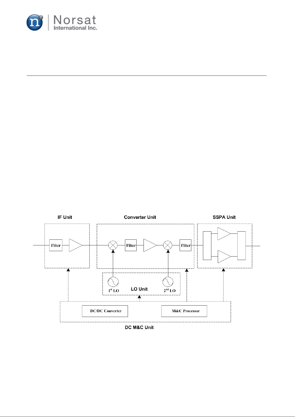
7020STC-O3b are comprised of IF, LO, Up-Converter, SSPA, and DC M&C as shown Fig. 1.
Figure 1. Functional Block Diagram of Ka-band 20W BUC
1.2.1 IF unit
© 2014 Norsat International Inc. Page 4 of 25
Page 5

IF unit amplifies the transmission signal from a remote modem and delivers it to the Up-converter
unit.
1.2.2 LO unit
LO unit generates two local signals to drive two LO ports of the up-converter using double
conversion structure.
1.2.3 Up-converter unit
Up-Converter converts the IF signal (A:1052-1788 MHz, B: 972-1871 MHz) to RF signal (A: 27.6 52-
28.388 GHz, B: 28.172-29.071 GHz) and also filters out unwanted spurious and harmonics in front
of SSPA. The BUC uses a double-conversion technology to achieve better performance and costeffective design.
1.2.4 SSPA unit
The main function of SSPA is to boost up the transmit power of the input signal to an expected level.
The SSPA includes the following modules: Divider, Power Amplifiers, and Combiner.
1.2.5 DC M&C unit
This board includes a DC/DC converter, regulators, and an EMI/EMC filter to make all kinds of DC
voltages required in the BUC. It also contains a Monitor and Control (M&C) function to monitor and
control the BUC, and communicate with a remote modem unit. The key parts for the M&C function
are a microprocessor and communication ICs for RS-232 and Ethernet.
1.3 CAUTIONS AND WARNINGS
Read all the following instructions prior to using the BUC.
1.3.1 Introduction
There is a potential safety risk unless appropriate precautions are taken while working with the BUC.
All the precaution and danger notes must be carefully read before beginning to use the BUC.
1.3.2 ESD Protection
The BUC contains elements sensitive to electrostatic discharges (ESD). It is important that the staff
is ground-connected while they are working with them.
1.3.3 Cleaning
Do not use liquid washing products or aerosols. Only use a damp cloth for cleaning.
1.3.4 Water
© 2014 Norsat International Inc. Page 5 of 25
Page 6

Do not expose the BUC to standing water. Failure to follow this precaution could result in electric
shock and injury to persons.
1.3.5 Installation of the BUC
The BUC described in this manual should not be installed in an unstable situation because it may
cause serious injuries to persons as well as a severe damage to the BUC.
1.3.6 Power Supply
An external power supply is necessary to convert the input AC to +48V DC, and for the internal
DC/DC converter within the BUC to generate appropriate DC voltages for IF, LO, Up-converter,
SSPA, and DC M&C units.
1.3.7 Equipment Working Conditions
Never perform maintenance or make adjustments to the BUC when the power supply is connected.
1.3.8 Important Safety Information
Read the chapters on Installation and System Operation before powering up the BUC.
Do not connect the AC INPUT (prime power) port to a power source until all the other connections
have been made.
1.3.9 Waveguide
Never operate the BUC without a cable or RF load connected to the RF OUTPUT waveguide.
Never stand in front of or look into the waveguide during BUC operations.
© 2014 Norsat International Inc. Page 6 of 25
Page 7
2. INTERFACES
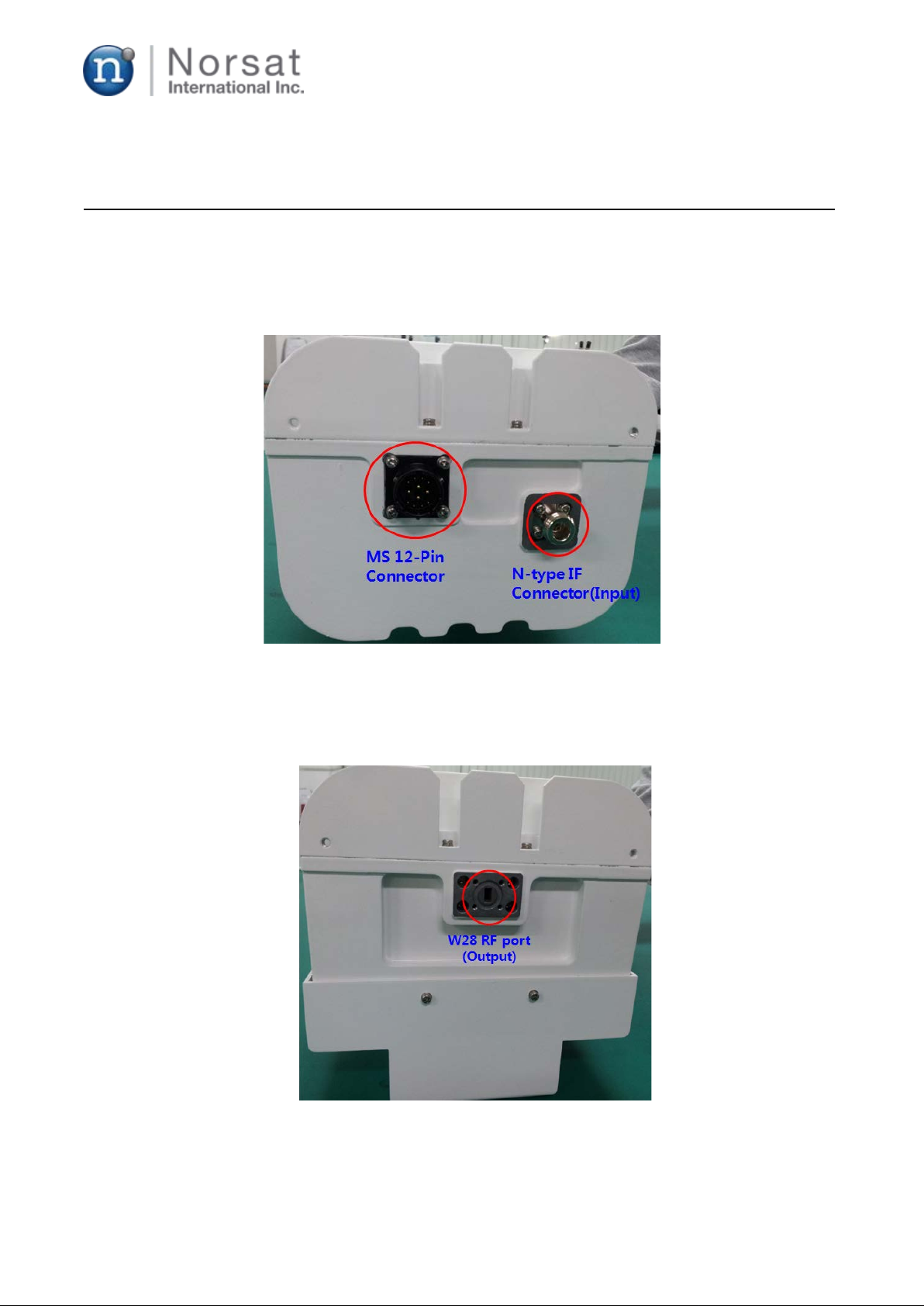
2.1 J1 / IF IN
N-type connector is used for the input port as shown in Fig. 2.
2.2 J2 / RF OUT
WR28 waveguide is used for the output port as shown in Fig. 3.
Figure 2. N-type IF and MS 12-pin connectors for Ka 20W BUC
Figure 3. WR28 RF output port for Ka 20W BUC
2.3 J3 / DC, M&C
© 2014 Norsat International Inc. Page 7 of 25
Page 8
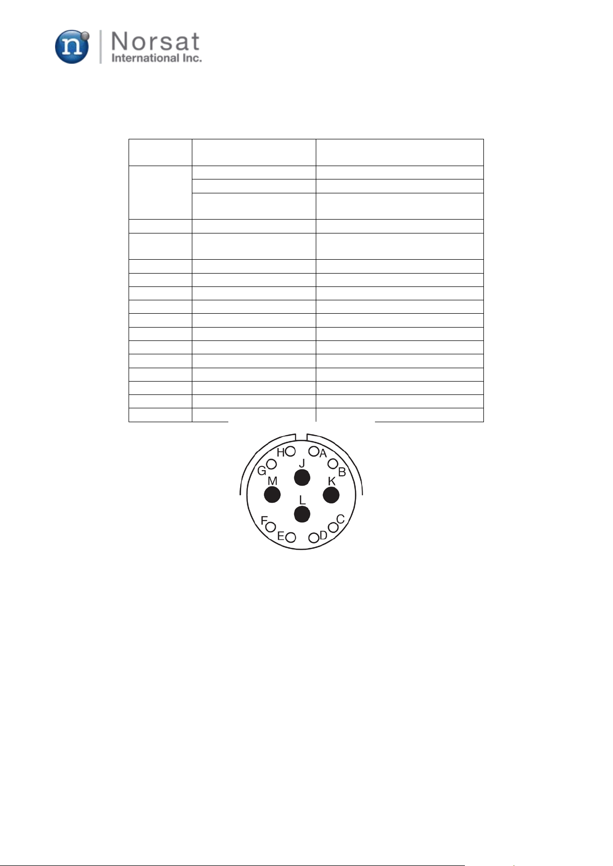
Connecto
r
IF input connector
N-female, panel-mounted
Impedance
50 ohm
10MHz reference
input
J2
RF output connector
WR28
DC / M&C(Ethernet or
RS232)
Panel-mount (MS3112e1412P)
J3-A
Ethernet Tx-
J3-B
Ethernet Tx+
J3-C
Ethernet Rx+
J3-D
Ethernet Rx-
J3-E
J3-F
RS-232 GND
J3-G
RS-232 TxD
J3-H
RS-232 RxD
J3-J
DC Power (+36 to +72V)
J3-K
DC Power return
J3-L
Mute @ High-Z or +5V
J3-M
Mute return (=RS-232 GND)
MS 12-pin connector is used for the DC and M&C port as shown in Fig. 2, and its pin map
and interface are indicated in Table 1 and Fig. 4, respectively.
Table 1 Pin description for IF, RF, M&C connectors
Parameter Description
J1
J3
Figure 4. Physical interface of MS 12-pin connector
© 2014 Norsat International Inc. Page 8 of 25
Page 9

3. TECHNICAL SPECIFICATIONS
3.1 SPECIFICATIONS SHEET
Output frequency A: 27.652 to 28.388 GHz
B: 28.172 to 29.071 GHz
Input frequency A: 1052 to 1788 MHz
B: 972 to 1871 MHz
L.O. frequency A: 26.6 GHZ, B: 27.20 GHz
Frequency conversion Double conversion
Frequency sense No inversion
Saturate Outpur power 43 dBm min. @ -40°C to +25 °C
42 dBM min. @ up to 55 °C
Maximum linear output power 41 dBm. min.
Input return loss 10 dB min
Output return loss 10 dB min
Phase noise (SSB) -73 dBc max at 1 KHz
-83 dBc max at 10 KHz
-93 dBc max at 100 kHz
External reference 10 MHz
signal frequency
External reference level -5 to +5 dBm
External reference phase noise -145 dBc max @ 1 KHz
Spectral Regrowth 25 dBc max @ 41 dBm
Group delay variation ±5.0 nanoseconds over an y
216MHz
Power Requirement +36 to +72V supplied through
MS connector
Power consumption 250W max.
Spurious
S ignal rel ated -60 dBc max at 38 dBm
Signal independant -60 dBc max
21F+LO -60 dBc max at 38 dBm
LO leakage -60 dBc max
Gain control 65 dB max (15dB, 1dB step)
Gain stability over temper ature ±2.5 dB at any constant
frequency
Gain flatness ±1.5 dB in any 216 MHz
±2.5 dB over full band
Input interface N-female
Output interface WR-28
Dimensions 300 (L) x 220 (W) x 150 (H) mm
Weight 6.5 kg
Operating Temp. -40 °C to +55 °C
Humidity 0 - 95 %
M & C Interface Ethernet or RS232 through
MS3112e14-12P connector
Output power
Temperature
LO Status
Output power mute
Gain control
© 2014 Norsat International Inc. Page 9 of 25
Page 10

3.2 OUTLINE DRAWING
Figure 5. Mechanical outline for Ka 20W BUC
© 2014 Norsat International Inc. Page 10 of 25
Page 11

4. INSTALLATION
This section of the manual is intended to provide aid in BUC installation.
4.1 UNPACKING
Perform an initial inspection upon receiving the BUC. You are advised to ensure the following:
Check that the shipping container is not opened or damaged.
Have a representative from the shipping company present if you suspect that the shipment
is damaged or tempered with before opening the container.
Check that all items in the packing list are present and undamaged.
If any loss or damage is discovered, contact NORSAT Inc. or a local representative before
proceeding.
The shipping container and packing materials should be retained for possible reshipment.
Accessories for 7020STC-O3b A or B are four waveguide adapter fixing screws, and an O-ring for
the waveguide adapter.
4.2 INSTALLATION ON ANTENNA
7020STC-O3b have two M4 threaded holes at each side of BUC as shown in Fig. 6 and these
holes are used to fix the mounting bracket when used as stand-alone unit. Please fix proper
brackets to four fixing holes on the BUC before mounting the BUC to the antenna. One of these
fixing holes can be used to connect the BUC housing to the earth for grounding.
Figure 6. Location of fixing holes on Ka 20W BUC
© 2014 Norsat International Inc. Page 11 of 25
Page 12

The BUC has body and cover heat sinks with fins as well as a fan for air cooling. Therefore, to
achieve an optimal function of the BUC, it should be mounted upside down so that fins of the body
heat sink and the air opening of the fan are open to fresh air as shown in Fig. 7. Ensure that there
are no objects that obstruct the flow of fresh air into the fins of the body heat sink and the air
opening of the fan.
Figure 7. Air cooling fins and fan of Ka 20W BUC
4.3 CABLE INSTALLATION
The connections of 7020STC-O3b A or B must be done using a waveguide (output) and coaxial
cables (input). The length of cables must be adjusted depending on the installation. An
inappropriate choice of the interface waveguide or cable may result in either a reduction of output
power at the external unit or an excessive distortion of the signal.
Some guidelines to install the interface cables between the internal units (Power supply and
Modem) and the external unit (BUC) are as follows:
a) Make a plan with the minimal route to be followed by the cables. It is recommended that 2m
of additional cable is added for ease of maintenance.
b) Secure the cables at each end of the connection.
c) Ensure that the external connectors are waterproof as well as resistant to other agents.
4.4 WATERTIGHT SEALING UP OF CABLES AND CONNECTORS
a) The application of moisture-resistant tape over the connectors is always recommended in
outdoor installations to ensure appropriate waterproofing. The application procedure of this
tape is the following: Ensure that all the connectors are correctly tightened. Cut a piece of
moisture-resistant tape with the desired size and remove the protector plastic of the tape.
© 2014 Norsat International Inc. Page 12 of 25
Page 13

b) Centre an end of the tape over the connector you want to protect and wrap tape tightly and
evenly over entire connector.
c) Repeat t he steps above for all the connectors
© 2014 Norsat International Inc. Page 13 of 25
Page 14

5. EQUIPMENT OPERATION
5.1 USER SOFTWARE INSTALLATION
The user software is a Windows based Graphical User Interface (GUI) to monitor and control the
BUC (A or B). It requires a dedicated RJ-45 (LAN port) or an RS-232 serial port (COM port) on the
PC to communicate with the BUC. If your PC has no serial port or RJ-45 port, an USB to RS232
adaptor is necessary to establish the connection (sold separately).
5.1.1 Installation Requirements
The user software installation requires Window XP or later versions with .NET Framework 4.0 preinstalled on your PC. The following list shows the minimum system requirements for installation:
∙ PC with an available RS-232 serial communication port or RJ-45 LAN communication port
∙ Microsoft Windows XP or later versions with .NET Framework 4.0 installed
∙ 1000MHz Processor
∙ RAM of 1024Mbytes
∙ Free hard disk space of at least 10Mbyte
∙ Monitor with 1024 x 768 screen resolution
5.1.2 Installation of the User Software
This GUI program is made up of just one executable file, ‘Ka 20W BUC GUI.exe’ but requires preinstalled .NET 4.0 Framework. If .NET Framework is missing from your system, it can be installed
by running “dotnetfx40.exe”. After successful installation of the .NET 4.0 Framework, run GUI
program.
5.2 USING BUC GUI
5.2.1 Description of BUC GUI Window
Brief description of the BUC GUI is as follows:
© 2014 Norsat International Inc. Page 14 of 25
Page 15

Figure 10. BUC GUI window for Ka band 20W BUC
① BUC Monitoring
This window shows the current status of BUC output power, LO lock status, temperature,
over temperature, over RF power, external mute, and Fan.
② Firmware Version Display
Firmware major version number (which means a number before dot in the version number)
must match that of GUI. For example if the firmware version is 2.X, GUI program version
should be 2.X.
③ Gain setting
This button is used to change the gain of the BUC
④ SSPA ON/ OFF function
This button is used to turn on or off the SSPA of the BUC.
⑤ UDP Command
This text box is used to control the BUC with commands via UDP (Ethernet) communication.
If you click command list button(
Commands list in 5.2.2)
⑥ Serial Command
This text box is used to control the BUC with commands via serial communication. If you
click command list button(
Commands list in 5.2.2)
⑦ DebugMode
This button is used to debug the BUC. It’s not used for operation.
⑧ Command List
This button shows the command list. (Refer to the serial Commands list in 5.2.2)
⑨ Status display window
This window shows the command processing result.
⑩ You can set up serial communication parameters.
(Usable serial port number, baud rate: 57600)
⑪ UDP Communication setting
You can set up UDP communication parameters.
⑧), You can see the command list. (Refer to the serial
⑧), You can see the command list. (Refer to the serial
© 2014 Norsat International Inc. Page 15 of 25
Page 16

Item
Command
Example
Explanation
1
gst
gst
Get BUC status
2
sspaon
sspaon
Turn on SSPA
3
sspaoff
sspaoff
Turn off SSPA
4
sendipwr
sendipwr 192 168 100 2
Write master(PC) ip
5
sendiprd
sendiprd
Read master ip
6
sendportwr
sendportwr 4001
Write master port
7
sendportrd
sendportrd
Read master port
8
ipwr
ipwr 192 168 100 10
Write BUC ip
9
iprd
iprd
Read BUC ip
10
portwr
portwr 3000
Write BUC port
11
portrd
portrd
Read BUC port
12
gwwr
gwwr 192 168 100 1
Write BUC gateway
13
gwrd
gwrd
Read BUC gateway
14
macwr
macwr 00 11 22 33 44 55
Write BUC MAC address
15
macrd
macrd
Read BUC MAC address
16
smwr
smwr 255 255 255 0
Write subnet mask
17
smrd
smwr
Read subnet mask
18
setgain
setgain 6500
Set up Max. gain
5.2.2 Serial and Ethernet Commands List
Table 2. Serial Commands List
5.2.3 Serial Mode Operation
For serial mode operation, connect a prepared RS232 cable between the MS 12-pin connector on
the BUC and the PC serial port as shown in Fig. 11. Refer to Table1 and Fig. 4 for RS232
connection.
Figure 11. RS 232 connection between BUC and PC
© 2014 Norsat International Inc. Page 16 of 25
Page 17

Run the BUC GUI. In this case, you can select only usable communication (COM) port on BUC
GUI window for connection.
Select a usable COM port and the baud rate of 57,600 and click the open button. If the COM port is
open, BUC GUI will show a firmware version number, and the LED color for SERIAL changes from
red into green and Enable is marked. BUC GUI starts reading status information of the BUC
periodically. And you can send control commands you want to the BUC by clicking proper tabs such
as MAX GAIN or SSPA ON or entering serial commands into the serial command text box
5.2.4 Ethernet Mode Operation
For Ethernet mode operation, connect a prepared Ethernet cable between the MS 12-pin connector
on the BUC and the PC Ethernet port as shown in Fig. 12 or Fig. 13. Refer to Table 1 and Fig. 4 for
Ethernet connection.
Figure 12. Ethernet connection between BUC and PC
Figure 13. Ethernet connection between BUC and PC via 10M or 10/100M Hub or Switch
Click BUC GUI icon on your PC and a BUC GUI window like Figure 10 shows up. However, unlike
serial mode connection, parameters for BUC and PC should be set up separately. And Ethernet
parameters setup for BUC should be done on your PC in the serial mode. The setup order for
Ethernet connection is as follows:
A. BUC parameters setup for Ethernet connection:
Parameters for BUC are sent to BUC when you enter necessary serial Commands into the serial
command text box and click the SEND tab in Fig. 10. Seven steps below are required to set up BUC
parameters for Ethernet connection.
© 2014 Norsat International Inc. Page 17 of 25
Page 18

Step 1. Set up BUC IP
- Serial command: ipwr 192 168 100 20 (Write Command)
- Serial command: iprd (Read Command)
Step 2. Set up BUC Port
- Serial command: portwr 4001 (Write Command)
- Serial command: portrd (Read Command)
Step 3. Set up Gateway
- Serial command: gwwr 192 168 100 1 (Write Command)
- Serial command: gwrd (Read Command)
Step 4. Set up Subnet Mask
- Serial command: smwr 255 255 255 0 (Write Command)
- Serial command: smrd (Read Command)
Step 5. Set up Mac address
- Serial command: macwr ff 11 dd 22 12 (as an example) (Write Command)
- Serial command: macrd (Read Command)
Step 6. S et up PC IP
- Serial command: sendipwr 192 168 100 10 (as an example) (Write Command)
- Serial command: sendiprd (Read Command)
In this step, you have to input IP of the computer which you’re using.
Step7. Set up PC Port
- Serial command: sendportwr 4001 (Write Command)
- Serial command: sendportrd (Read Command)
B. PC parameters setup for Ethernet connection:
There are two steps to perform for PC parameters setup for Ethernet connection.
Step 8. Set up PC parameters
The BUC IP, BUC PORT, and PC PORT number should be entered into the Ethernet
parameters
boxes on BUC GUI window as shown in Fig. 10.
© 2014 Norsat International Inc. Page 18 of 25
Page 19

Step 9. Click OPEN
If the Ethernet port is open, BUC GUI will show a firmware version number, and the LED color for
ETHERNET changes from red into green and Enable is marked as shown in Figure 10. BUC GUI
starts reading status information of the BUC periodically. And you can send control commands you
want to the BUC by clicking proper tabs such as MAX GAIN or SSPA ON or entering UDP
commands into the UDP command text box.
5.2.5 BUC Turn-on/off Sequence.
After the user software is installed on your PC, the following sequence can be used to turn on the
BUC.
1) Connect one end of a RF cable with a WR28 waveguide adapter to WR28 RF port on the
BUC and the other end of the RF cable to the antenna or a dummy load.
2) Connect one end of an IF cable to N-type IF connector on the BUC and the other end of the
IF cable to the output of the IF source or modem.
3) Connect one end of a MS 12-wires cable to MS 12-pins connector on the BUC. And connect
two wires out of the other end of the MS 12-wires cable, which are dedicated to DC power,
to a power supply with +48V DC or a level specified in the specification sheet in Section 3.1,
and four wires for Ethernet connection or three wires for RS232 connection out of the other
end of the MS 12-wires cable to the modem or your PC, and external Mute wire to a ground.
(Refer to Table 1 and Fig. 4 for connection details)
4) Turn on the power supply to supply +48V to the BUC.
5) Set up the serial mode or Ethernet mode connection according to Section 5.2.3 or 5.2.4.
6) Once your PC or modem is connected with the BUC using either serial or Ethernet mode,
check various BUC status such as Output power, Temperature, LO Lock, Over-temperature,
Over-power, Fan, and external mute.
7) Turn on the IF power source with a proper power level according to the BUC specification
sheet, which enters the IF input port of the BUC.
8) To turn on the SSPA, make sure that all of LO Lock, Over-temperature, Over-power, and
External Mute states should be green. Then click SSPA ON button on BUC GUI window.
9) Adjust the BUC gain using Gain setting buttons such as MAX GAIN, MIN GAIN, and specific
gain values on the BUC GUI window.
10) If all of LO Lock, Over-temperature, Over-power, and External Mute states are not gre en on
BUC GUI window, the SSPA does not turn on even though SSPA ON button is clicked.
During the operation, if one of LO Lock, Over-temperature, Over-power, and External Mute
states becomes red on BUC GUI window, the SSPA is automatically turned off.
© 2014 Norsat International Inc. Page 19 of 25
Page 20

11) If you want to turn off the SSPA, just click SSPA MUTE button or pull out the External Mute
signal wire from the ground.
6. MAINTENANCE AND TROUBLE SHOOTING
6.1 MAINTENANCE
Ka band 20W BUC has body and cover heat sinks with fins as well as a fan for air cooling.
Therefore, to achieve an optimal function of the BUC, it should be mounted upside down so that fins
of the body heat sink and the air opening of the fan are open to fresh air as shown in Fig. 7. Check
periodically that there are no objects obstructing the flow of fresh air into the fins of the body heat
sink and the air opening of the fan. And also periodic maintenance to clean the fan dust is required.
6.2 TROUBLE SHOOTING
The BUC GUI window shows various status of the BUC such as LO Lock, Over-temperature, Over-
power, and External Mute. These states indicate the faults that may arise in the BUC. The BUC is
designed to automatically turn on the SSPA to avoid transmitting unwanted power to the target
satellite if one of LO Lock, Over-temperature, Over-power, and External Mute states becomes red
on BUC GUI window during the operation.
The following explains two major types of faults and how to troubleshoot them.
A) SSPA is off
1) When LO Lock state became red on the BUC GUI window.
- The internal LOs are out of lock.
Check the power level of 10MHz reference source at the modem side or at the BUC
input side.
Otherwise, since the BUC is faulty, contact NORSAT for further support.
2) When Over-temperature state became red on the BUC GUI window.
- The BUC is faulty if the BUC is hot
Contact NORSAT for further support
- M&C processor is temporally malfunctioning if the BUC is hot.
Turn off the main power supply of +48V and wait for about 5 minutes, and then turn
© 2014 Norsat International Inc. Page 20 of 25
Page 21

on again and check the Over-temperature state on the BUC GUI window.
3) When Over-power became red on the BUC GUI window.
- IF input power is too high
Check the IF input power level.
- Or, the BUC is faulty
Contact NORSAT for further support.
4) When External Mute became red on the BUC GUI window.
- External Mute pin is not connected to ground.
Check the External Mute wire connected to ground.
- Or, the BUC is faulty
Contact NORSAT for further support
B) RF output power is low even if SSPA is on
1) Gain setting on the BUC GUI window is too low
Check gain setting on the BUC GUI.
2) Input IF power is too low to drive the BUC properly
Check the output level of the IF power source.
3) IF cable or connectors has high insertion loss
Check the IF cable or connectors.
4) RF cable or connector or WR28 waveguide adapter has high insertion loss
Check the RF cable, connector, or WR28 waveguide adapter.
5) One of internal components are faulty
Contact NORSAT for further support.
© 2014 Norsat International Inc. Page 21 of 25
Page 22

© 2014 Norsat International Inc. Page 22 of 25
Page 23

7. WARRANTY AND SERVICE INFORMATION
All the equipment (BUC) supplied or manufactured fulfils the following warranty conditions except
when other conditions are specified at the moment of purchasing.
Warranty limit: The seller guarantees that every item supplied by the manufacturer is free of
mistakes or human manipulation. This warranty is not applied to those materials or components that
are not supplied by the manufacturer or those that have been exposed to possible damaging
situations or those that are not manipulated under the security conditions described in the user
manual.
The standard length of the warranty is two (2) years, except if otherwise established at the time of
purchase.
Repair conditions: Items returned will be tested in order to determine the fault in the
equipment.The replacement or return will be established once the manufacturer has determined the
cause of the fault. All the equipment returned is subject to a charge for its evaluation when the
warranty cover is not applicable for any reason or when the client authorizes the repair out of
warranty.
Remember that if a failure in the equipment is not found the client will be the responsible for paying
the cost of testing the item.
Delivery charges: Clients will be responsible for the delivery charges, except if there is a previous
agreement.
© 2014 Norsat International Inc. Page 23 of 25
Page 24

8. CUSTOMER SERVICE
8.1 Warranty Repair
If the unit fails due to defects in materials or workmanship, NORSAT Inc. will, at its sole discretion,
repair or replace the defective parts, free of charge, for two (2) years from the date of its shipment
from NORSAT factory.
Note. Warranty does not cover the cost of shipment to and from NORSAT Inc.
8.2 Exceptions to Warranty
NORSAT Inc. shall have no liability or obligation to Purchaser with respect to the product subjected
to any of the following:
1. Damage during shipment.
2. Failure caused by products not supplied by NORSAT Inc. its authorized contractors or agents.
3. Failure caused by operation of the product outside its published electrical or environmental
specifications, or any causes other than ordinary use.
8.3 Other Repairs
Non-warranty and out-of-warranty repair service is available from NORSAT Inc. The repair service
can be obtained by contacting NORSAT Inc. A Return Material Authorization (RMA) number must
be obtained.
8.4 Product Return Procedure
For repairs, please contact NORSAT Inc. to obtain a RMA (Return Material Authorization) number.
The RMA tag will have to be filled in and attached to the unit before shipping it to NORSAT Inc.
8.5 Contact
Address: Norsat International Inc.
110-4020 Viking Way
Richmond, BC
CANADA V6V 2L4
tel: +1 604 821 2800
fax: +1 604 821 2801
© 2014 Norsat International Inc. Page 24 of 25
Page 25

9. APPENDIX
9.1 ACRONYMS AND ABBREVIATIONS
The following acronyms are used in this document:
AC Alternating Current
BUC Block Up Converter
DC Direct Current
GND Ground
ESD Electrostatic discharges
IC Integrated Circuit
IF Intermediate Frequency
IN Input
LO Local Oscillator
M&C Monitor and Control
OUT Output
PC Personal Computer
RF Radio Freq uency
Rx Reception
SSPA Solid State Power Amplifier
Tx Transmission
© 2014 Norsat International Inc. Page 25 of 25
 Loading...