

Page 1

nRF52 Preview Development
Kit
User Guide
v1.2
4397_497 v1.2 / 2017-02-15
Page 2

Contents
Revision history. . . . . . . . . . . . . . . . . . . . . . . . . . . . . . . . . . iii
1 Introduction. . . . . . . . . . . . . . . . . . . . . . . . . . . . . . . . . . . 4
2 Setting up the development kit. . . . . . . . . . . . . . . . . . . . . . . . 6
3 Software tools. . . . . . . . . . . . . . . . . . . . . . . . . . . . . . . . . . 7
4 Start developing. . . . . . . . . . . . . . . . . . . . . . . . . . . . . . . . . 8
5 Interface MCU. . . . . . . . . . . . . . . . . . . . . . . . . . . . . . . . . . 9
5.1 IF Boot/Reset button . . . . . . . . . . . . . . . . . . . . . . . . . . . . . . . 9
5.2 Virtual COM port . . . . . . . . . . . . . . . . . . . . . . . . . . . . . . . . 9
5.3 Interface MCU firmware (FW) . . . . . . . . . . . . . . . . . . . . . . . . . . . 10
5.4 MSD . . . . . . . . . . . . . . . . . . . . . . . . . . . . . . . . . . . . . 10
6 Hardware description. . . . . . . . . . . . . . . . . . . . . . . . . . . . . 12
6.1 Hardware drawings . . . . . . . . . . . . . . . . . . . . . . . . . . . . . . . 12
6.2 Block diagram . . . . . . . . . . . . . . . . . . . . . . . . . . . . . . . . . 13
6.3 Power supply . . . . . . . . . . . . . . . . . . . . . . . . . . . . . . . . . . 13
6.4 Connector interface . . . . . . . . . . . . . . . . . . . . . . . . . . . . . . . 15
6.5 Buttons and LEDs . . . . . . . . . . . . . . . . . . . . . . . . . . . . . . . . 17
6.5.1 I/O expander for buttons and LEDs . . . . . . . . . . . . . . . . . . . . . . . 18
6.6 32.768 kHz crystal . . . . . . . . . . . . . . . . . . . . . . . . . . . . . . . . 20
6.7 Measuring current . . . . . . . . . . . . . . . . . . . . . . . . . . . . . . . 21
6.8 RF measurements . . . . . . . . . . . . . . . . . . . . . . . . . . . . . . . . 22
6.9 Debug input . . . . . . . . . . . . . . . . . . . . . . . . . . . . . . . . . . 23
6.10 Debug output . . . . . . . . . . . . . . . . . . . . . . . . . . . . . . . . . 24
6.11 NFC antenna interface . . . . . . . . . . . . . . . . . . . . . . . . . . . . . 25
Legal notices. . . . . . . . . . . . . . . . . . . . . . . . . . . . . . . . . . . 27
4397_497 v1.2
ii
Page 3

Revision history
Date Version Description
February 2017 1.2
• Created PDF
• Added MSD on page 10
• Updated Interface MCU firmware (FW) on page 10
4397_497 v1.2
iii
Page 4

1
Introduction
In addition to hardware, the nRF52 Preview Development Kit consists of firmware source code,
documentation, hardware schematics, and layout files.
The key features of the development kit are:
• nRF52832 flash-based ANT/ANT+, Bluetooth® Low Energy SoC solution
• Buttons and LEDs for user interaction
• I/O interface for Arduino form factor plug-in modules
• SEGGER J-Link OB Debugger with debug out functionality
• Virtual COM Port interface via UART
• Drag-and-drop Mass Storage Device (MSD) programming
• Supporting NFC-A listen mode
For access to firmware source code, hardware schematics, and layout files, see www.nordicsemi.com.
Figure 1: 1 × nRF52 Preview Development Kit board (PCA10036) and 1 × NFC adhesive tag
4397_497 v1.2
4
Page 5

Introduction
4397_497 v1.2
5
Page 6

2
Setting up the development kit
Before you start developing, prepare your development kit hardware by completing a few easy steps and
download the required software.
1. To set up the hardware, follow the instructions in Getting started with the nRF52 Development Kit.
2. Download and install the software tools.
a) nRFgo Studio. Download and install nRFgo Studio (which includes the nRF Tools package; JLinkARM,
JLink CDC, nRFjprog, and mergehex) from nRFgo Studio.
b) Keil MDK-ARM. Download and install the latest Keil MDK-ARM from Keil MDK-ARM Development
Kit.
c) nRF5 SDK. Download and extract the latest nRF5 SDK found on developer.nordicsemi.com.
d) Keil Device Family Pack. Install the Device Family Pack that is shipped with the SDK, or let Keil install
it automatically.
e) SDK documentation. Read the information in the SDK Release Notes, and check the nRF5 SDK
documentation.
4397_497 v1.2
6
Page 7

3
Software tools
We have an extensive range of supporting software tools to help you with testing and programming on
your chip.
• nRFgo Studio: This is our tool for programming and configuring devices. It supports the programming
of nRF52 SoftDevices, applications, and bootloaders.
• nRF5 SDK: The nRF5 Software Development Kit (SDK) provides source code of examples and libraries
forming the base of your application development.
• nRF5x tools: nRF5x Tools is a package that contains JLinkARM, JLink CDC, nRFjprog, and mergehex. The
nRFjprog is a command line tool for programming nRF5x series chips. It is also useful in a production
setup. nRF5x Tools will be installed together with nRFgo Studio.
• Master Control Panel: The Master Control Panel is a software tool that is used to act as a Bluetooth
Low Energy peer device.
• Master Control Panel: (64-bit version) (32-bit version) The Master Control Panel is a software tool
that is used with the nRF51 Dongle (PCA10031) to act as a Bluetooth Low Energy peer device. You
can test your application’s wireless connection with this tool. The Master Control Panel supports
programming of SEGGER J-Link based nRF52 devices. For more information, see the help files in the
Master Control Panel.
• nRF Master Control Panel for Android 4.3 or later: nRF Master Control Panel for Android 4.3
or later is a powerful generic tool that allows you to scan and explore your Bluetooth Smart
devices and communicate with them on an Android phone. MCP supports a number of Bluetooth
SIG adopted profiles together with the Device Firmware Update (DFU) profile from Nordic
Semiconductor.
• S132 SoftDevice: Bluetooth Smart concurrent multi-link protocol stack solution supporting
simultaneous Central, Peripheral, Broadcaster, and Observer roles. For more information, see the S132
SoftDevice Specification and the nRF5 SDK documentation.
We also recommend some third party software tools that are useful when developing with our products:
• Keil MDK-ARM Development Kit: Keil MDK-ARM Development Kit is a development environment
specifically designed for microcontroller applications that lets you develop using the nRF52 SDK
application and example files.
• SEGGER J-Link Software: The J-Link software is required to debug using the J-Link hardware that is
packaged with our development kits.
• ANTware II: ANTWare is an application used for the control of ANT wireless devices. It is an excellent
tool for first time ANT developers to explore the capabilities of ANT as a low power wireless solution,
and for experienced users to easily setup and monitor advanced ANT networks. ANTWare II improves
upon past versions with a slick new interface, streamlined functions, and a variety of new features.
4397_497 v1.2
7
Page 8

4
Start developing
After you have set up the development kit and installed the toolchain, it is time to start developing.
There are several ways to continue from here:
• Running precompiled examples
See the step by step instructions on how you can quickly test a precompiled example without having
to use the full toolchain, it is a matter of copying and pasting a precompiled hex file onto your
development kit board.
• Compiling and running a first example
Test that you have set up your toolchain correctly by compiling, programming and running a very
simple example.
• Running examples that use a SoftDevice
Before you can run more advanced examples that use Bluetooth or ANT, you must first program the
SoftDevice on the board.
4397_497 v1.2
8
Page 9

5
Interface MCU
The Interface MCU is used to control the firmware on the nRF52832 IC by the on-board SEGGER J-Link.
Figure 2: Interface MCU
5.1 IF Boot/Reset button
The nRF52 Preview Development Kit board is equipped with a boot/reset button (SW5).
This button is connected to the Interface MCU on the board and has two functions:
• Resetting the nRF52832 device.
• Entering bootloader mode of the interface MCU.
During normal operation the button will function as a reset button for the nRF52832 device. For this
to work, pin reset on P0.21 needs to be enabled for the nRF52832 device. The button is also used to
enter the bootloader mode of the Interface MCU. To enter bootloader mode, keep the reset button
pressed while powering up the board until LED (LD5) starts to blink. You can power up the board either by
disconnecting and reconnecting the USB cable, or toggle the power switch (SW6).
Important: Pin reset can be enabled by defining the CONFIG_GPIO_AS_PINRESET variable
in the project settings. This can be done by defining the preprocessor symbol in Keil, go to:
Project > Options for Target > C/C++ > Preprocessor Symbols > Define. Here you can add the
CONFIG_GPIO_AS_PINRESET variable after NRF52.
This functionality can be removed by doing a nRFjprog --recover.
5.2 Virtual COM port
The on-board Interface MCU features a Virtual COM port via UART.
The virtual COM port has the following features:
4397_497 v1.2
9
Page 10
Interface MCU
• Flexible baudrate setting up to 1 Mbps.
• Dynamic Hardware Flow Control (HWFC) handling.
• Tri-stated UART lines when no terminal is connected.
Table 1: Relationship of UART connections on nRF52832 and Interface MCU on page 10 shows an
overview of the UART connections on nRF52832 and the interface MCU.
Default GPIO nRF52832 UART nRF52832 Interface MCU UART
P0.05 RTS CTS
P0.06 TXD RXD
P0.07 CTS RTS
P0.08 RXD TXD
Table 1: Relationship of UART connections on nRF52832 and Interface MCU
The UART signals are routed directly to the Interface MCU. The UART pins connected to the Interface MCU
are tri-stated when no terminal is connected to the Virtual COM port on the computer.
Important: The terminal used must send a DTR signal in order to configure the UART Interface
MCU pins.
The P0.05 (RTS) and P0.07 (CTS) can be used freely when HWFC is disabled on the nRF52832.
5.3 Interface MCU firmware (FW)
The on-board interface MCU is factory programmed with an mbed-compliant bootloader. This makes it
possible to update the SEGGER J-Link OB interface firmware.
For more information on entering the bootloader mode, see IF Boot/Reset button on page 9.
To update Interface MCU firmware, drag the Interface image (.bin) into the mounted bootloader drive on
the connected computer and power cycle the board. It is also possible to download the latest SEGGER JLink software from SEGGER J-Link Software and open a debug session in order to automatically update to
the latest J-Link OB firmware version.
The J-Link OB image can be downloaded from www.nordicsemi.com.
Important: When in bootloader mode, do not drag and drop any file except those downloaded
from www.nordicsemi.com for use with the Interface MCU. If a wrong file is used, it can overwrite
the bootloader and ruin the Interface MCU firmware without the possibility of recovery.
5.4 MSD
The interface MCU features a mass storage device (MSD). This makes the development kit appear as an
external drive on your computer.
This drive can be used for drag-and-drop programming. Files cannot be stored on this drive. By copying a
HEX file to the drive, the interface MCU will program the file to the device.
4397_497 v1.2
10
Page 11

Interface MCU
Important:
• Windows might try to defragment the MSD part of the interface MCU. If this happens, the
interface MCU will disconnect and be unresponsive. To return to normal operation, the
development kit must be power cycled.
• Your antivirus software might try to scan the MSD part of the interface MCU. It is known that a
certain antivirus program triggers a false positive alert in one of the files and quarantines the
unit. If this happens, the interface MCU will become unresponsive.
• If the computer is set up to boot from USB, it can try to boot from the development kit if
the development kit is connected during boot. This could be avoided by unplugging the
development kit before a computer restart, or changing the boot sequence of the computer.
You can also disable the MSD of the kit by using the msddisable command in J-Link Commander.
To enable, use the msdenable command. These commands take effect after a power cycle of the
development kit and should stay this way until changed again.
4397_497 v1.2
11
Page 12

6
Hardware description
The nRF52 Preview Development Kit board (PCA10036) can be used as a development platform for the
nRF52832 device. It features an onboard programming and debugging solution.
In addition to radio communication, the nRF52832 device can communicate with a computer through a
virtual COM port provided by the interface MCU.
6.1 Hardware drawings
nRF52 Preview Development Kit hardware drawings show both sides of the PCA10036 board.
Figure 3: nRF52 Preview Development Kit board top view
Figure 4: nRF52 Preview Development Kit board bottom view
4397_497 v1.2
12
Page 13

Hardware description
6.2 Block diagram
The nRF52 Preview Development Kit board block diagram shows the connections between the different
blocks.
External supply
Current
measurement
USB
Battery
Buttons
Voltage regulator
LEDs
GPIO
nRF52832
PCB
Antenna
Interface MCU
VBUS
USB sense
Data
Osc
32.768 kHz
IF Boot/Reset
UART
SWD
VCC_nRF
Osc
32 MHz
Debug inDebug out
Power switch
Power switch
Matching
network
NFC antenna
SWF switch/
RF connector
I/O
expander
Debouncing
filter
Switch
Switch
Figure 5: nRF52 Preview Development Kit board block diagram
6.3 Power supply
The nRF52 Preview Development Kit board has three power options: 5 V from the USB, external power
supply, and coin cell battery.
4397_497 v1.2
13
Page 14

Hardware description
Figure 6: Power supply options
The 5 V from the USB is regulated down to 3.3 V through an on-board voltage regulator. The battery and
external power supply are not regulated. The power sources are routed through a set of diodes (D1A, D1B,
and D1C) for reverse voltage protection, where the circuit is supplied from the source with the highest
voltage.
Important: When USB is not powered, the Interface MCU is in dormant state and will draw
an additional current of ~ 20 μA in order to maintain the reset button functionality. This will
affect board current consumption, but not the nRF52832 current measurements, as described in
Measuring current on page 21.
Figure 7: Power supply circuitry
The reverse voltage protection diodes will add a voltage drop to the supply voltage of the circuit. To avoid
this voltage drop, the diodes can be bypassed by shorting one or more solder bridges.
4397_497 v1.2
14
Page 15

Hardware description
Power source Protection bypass Voltage level
USB SB10 3.3 V
Coin-cell battery SB11 Battery
External supply SB12 1.7 V - 3.6 V
Table 2: Protection diode bypass solder bridges
Figure 8: Protection diode bypass solder bridges
Important: Connect only one power source at the time. Shorting the solder bridges removes the
reverse voltage protection.
6.4 Connector interface
Access to the nRF52832 GPIOs is available from connectors P2, P3, P4, P5, and P6. The P1 connector
provides access to ground and power on the nRF52 Preview Development Kit board.
4397_497 v1.2
15
Page 16

Hardware description
Figure 9: nRF52 Preview Development Kit board connectors
The signals are also available on connectors P7, P8, P9, P10, P11, and P12, which are on the bottom side
of the board. By mounting pin lists on the connector footprints, the nRF52 Preview Development Kit board
can be used as a shield for Arduino motherboards or other boards that follow the Arduino standard.
For easy access to GPIO, power, and ground, the signals can also be found on the through-hole connectors
P13–P17.
Important: Some pins have default settings.
• P0.00 and P0.01 are by default used for the 32 kHz crystal and are not available on the
connectors. For more information, see Section 32.768 kHz crystal on page 20.
• P0.05, P0.06, P0.07, and P0.08 are by default used by the UART connected to the Interface
MCU. For more information, see Section Virtual COM port on page 9.
• P0.09 and P0.10 are by default used by NFC1 and NFC2. For more information, see Section NFC
antenna interface on page 25.
• P0.13–P0.20 are by default connected to the buttons and LEDs. For more information, see
Section Buttons and LEDs on page 17.
When the nRF52 Preview Development Kit board is used as a shield together with an Arduino standard
motherboard, the Arduino signals are routed as shown in Figure 10: Arduino signals routing on the nRF52
Preview Development Kit board on page 17.
4397_497 v1.2
16
Page 17

Hardware description
Figure 10: Arduino signals routing on the nRF52 Preview Development Kit board
6.5 Buttons and LEDs
The four buttons and four LEDs on the nRF52 Preview Development Kit board are connected to dedicated
I/Os on the nRF52832 chip.
Part GPIO Short
Button 1 P0.13 -
Button 2 P0.14 -
Button 3 P0.15 -
Button 4 P0.16 -
LED 1 P0.17 SB5
LED 2 P0.18 SB6
LED 3 P0.19 SB7
LED 4 P0.20 SB8
Table 3: Button and LED connection
If GPIO P0.17–P0.20 are needed elsewhere, the LEDs can be disconnected by cutting the short on
SB5–SB8, see Figure 11: Disconnecting the LEDs on page 18. The LEDs and buttons can also be
disconnected by using the I/O extender as described in I/O expander for buttons and LEDs on page 18.
4397_497 v1.2
17
Page 18

Hardware description
Figure 11: Disconnecting the LEDs
The buttons are active low, meaning the input will be connected to ground when the button is activated.
The buttons have no external pull-up resistor, so to use the buttons the P0.13–P0.16 pins must be
configured as an input with an internal pull-up resistor.
The LEDs are active low, meaning that writing a logical zero ('0') to the output pin will illuminate the LED.
Figure 12: Button and LED configuration
6.5.1 I/O expander for buttons and LEDs
The nRF52 Preview Development Kit board has an I/O expander to avoid conflicts with boards that follow
the Arduino standard, the on-board GPIOs for the buttons and LEDs would otherwise possibly conflict with
such boards.
4397_497 v1.2
18
Page 19

Hardware description
GPIO Part Arduino signal
P0.13 Button 1 2
P0.14 Button 2 3
P0.15 Button 3 4
P0.16 Button 4 5
P0.17 LED 1 6
P0.18 LED 2 7
P0.19 LED 3 8
P0.20 LED 4 9
Table 4: GPIO connection
The I/O expander will release these GPIOs for general use when the nRF52 Preview Development Kit
is used together with boards that follows the Arduino standard. The I/O expander can be permanently
enabled by shorting solder bridge SB18 or permanently disabled by cutting the shorting track on SB19. You
must also short SB18 when cutting SB19 for full compatibility with the Arduino standard.
The I/O extender can be temporarily enabled by connecting SHIELD DETECT to ground.
Figure 13: Enable or disable I/Os for Arduino standard
In addition to the buttons and LEDs, the following GPIOs are used for the I/O expander:
I/O expander signal GPIO
/INT P0.17
SDA P0.26
SCL P0.27
Table 5: I/O expander connection
4397_497 v1.2
19
Page 20

Hardware description
Figure 14: I/O expander schematic
Important: SW debouncing should not be needed when using the I/O expander. Each button on
the nRF52 Preview Development Kit board is equipped with a debouncing filter.
6.6 32.768 kHz crystal
nRF52832 can use an optional 32.768 kHz crystal (X2) for higher accuracy and lower average power
consumption.
On the nRF52 Preview Development Kit board, P0.00 and P0.01 are by default used for the 32.768 kHz
crystal and are not available as a GPIO on the connectors.
Important: When using ANT/ANT+, the 32.768 kHz crystal (X2) is required for correct operation.
If P0.00 and P0.01 are needed as normal I/Os, the 32.768 kHz crystal can be disconnected and the GPIO
routed to the connectors. Cut the shorting track on SB1 and SB2, and solder SB3 and SB4. See Figure 15:
Configuring P0.00 and P0.01 on page 20 for reference.
Figure 15: Configuring P0.00 and P0.01
4397_497 v1.2
20
Page 21

Hardware description
Figure 16: 32.768 kHz crystal and SB1 to SB4 schematic
6.7 Measuring current
The current drawn by the nRF52832 device can be monitored on the nRF52 Preview Development Kit
board.
To measure the current, you must first prepare the board by cutting the shorting of solder bridge SB9.
There are two ways of measuring the current consumption: using an ampere-meter or an oscilloscope.
1. Ampere-meter:
a. Connect an ampere-meter between the pins of connector P22. This will monitor the current
directly.
Figure 17: Current measurement with ampere-meter
2. Oscilloscope:
a. Mount a resistor on the footprint for R6. The resistor should not be larger than 10 Ω.
b. Connect an oscilloscope in differential mode or similar with two probes on the pins of the P22
connector.
c. Measure the voltage drop. The voltage drop will be proportional to the current consumption. For
example, if a 10 Ω resistor is chosen, 10 mV equals 1 mA.
4397_497 v1.2
21
Page 22

Hardware description
Figure 18: Current measurement with oscilloscope
Important: The current measurements will become unreliable when a serial terminal is connected
to the Virtual COM port.
6.8 RF measurements
The nRF52 Preview Development Kit board is equipped with a small size coaxial connector (J1) for
conducted measurements of the RF signal.
The connector is of SWF type from Murata (part no. MM8130-2600) with an internal switch. By default,
when there is no cable attached, the RF signal is routed to the on-board PCB trace antenna.
A test probe is available from Murata (part no. MXHS83QE3000) with a standard SMA connection on the
other end for connecting instruments. When connecting the test probe, the internal switch in the SWF
connector will disconnect the PCB antenna and connect the RF signal from the nRF52832 device to the
test probe.
4397_497 v1.2
22
Page 23

Hardware description
Figure 19: Connecting a spectrum analyzer
The connector and test probe will add loss to the RF signal which should be taken into account when doing
measurements, see Table 6: Typical loss in connector and test probe on page 23.
Frequency (MHz) Loss (dB)
2440 1.0
4880 1.7
7320 2.6
Table 6: Typical loss in connector and test probe
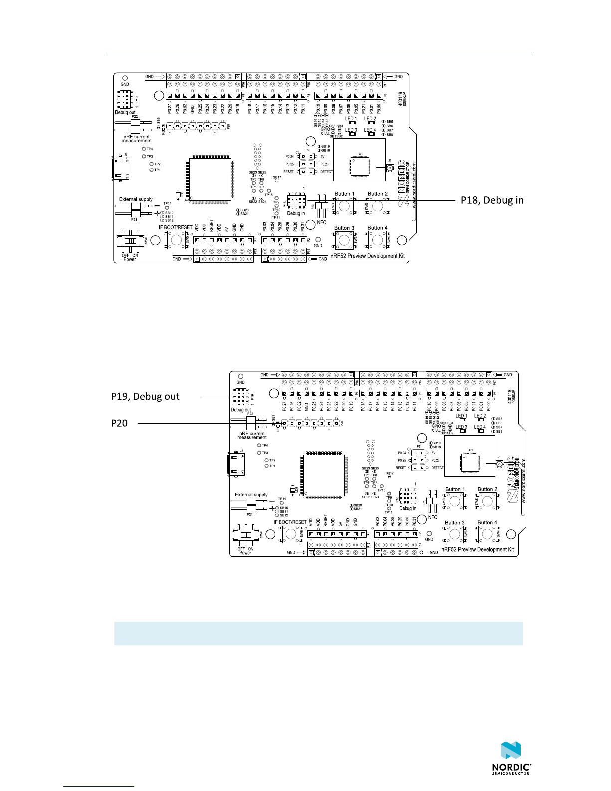
6.9 Debug input
The Debug in connector (P18) makes it possible to connect external debuggers for debugging while
running on battery or external power supply.
4397_497 v1.2
23
Page 24
Hardware description
Figure 20: Debug input connector
6.10 Debug output
The nRF52 Preview Development Kit board supports programming and debugging external boards. To
debug an external board, connect to the Debug out connector (P19) with a 10 pin cable.
Figure 21: Debug output connector
When the external board is powered, the interface MCU will detect the supply voltage of the board and
program/debug the target chip on the external board instead of the on-board nRF52832.
Important: The voltage supported by external debugging/programming is 3.0 V.
You can also use P20 as a debug out connection to program shield mounted targets. For the Debug out
header (P19), the Interface MCU will detect the supply voltage on the mounted shield and program/debug
the shield target.
If the Interface MCU detects target power on both P19 and P20, it will by default program/debug the
target connected to P19.
4397_497 v1.2
24
Page 25

Hardware description
6.11 NFC antenna interface
The nRF52 Preview Development Kit board supports a Near Field Communication (NFC) tag.
NFC-A listen mode operation is supported on nRF52832. The NFC antenna input is available on connector
P23 on the nRF52 Preview Development Kit board.
Figure 22: NFC antenna connector
NFC uses two pins, pin 11 (NFC1) and pin 12 (NFC2) to connect the antenna. These pins are shared with
GPIOs (P0.09 and P0.10) and the PROTECT field in the NFCPINS register in UICR defines the usage of these
pins and their protection level against abnormal voltages. The content of the NFCPINS register is reloaded
at every reset.
Important: The NFC pins are enabled by default. NFC can be disabled and GPIOs enabled by
defining the CONFIG_NFCT_PINS_AS_GPIOS variable in the project settings. This can be done
by defining the preprocessor symbol in Keil, go to: Project > Options for Target > C/C++ >
Preprocessor Symbols > Define. Here you can add the CONFIG_NFCT_PINS_AS_GPIOS variable
after NRF52.
This functionality can be removed by doing a nRFjprog --recover.
Pin 11 and pin 12 are by default configured to use the NFC antenna, but if pin 11 and pin 12 are needed as
normal GPIOs, R25 and R26 must be relocated to R27 and R28.
4397_497 v1.2
25
Page 26

Hardware description
Figure 23: NFC input schematic
4397_497 v1.2
26
Page 27

Legal notices
By using this documentation you agree to our terms and conditions of use. Nordic Semiconductor may
change these terms and conditions at any time without notice.
Liability disclaimer
Nordic Semiconductor ASA reserves the right to make changes without further notice to the product to
improve reliability, function or design. Nordic Semiconductor ASA does not assume any liability arising out
of the application or use of any product or circuits described herein.
All information contained in this document represents information on the product at the time of
publication. Nordic Semiconductor ASA reserves the right to make corrections, enhancements, and other
changes to this document without notice. While Nordic Semiconductor ASA has used reasonable care
in preparing the information included in this document, it may contain technical or other inaccuracies,
omissions and typographical errors. Nordic Semiconductor ASA assumes no liability whatsoever for any
damages incurred by you resulting from errors in or omissions from the information included herein.
Life support applications
Nordic Semiconductor products are not designed for use in life support appliances, devices, or systems
where malfunction of these products can reasonably be expected to result in personal injury.
Nordic Semiconductor ASA customers using or selling these products for use in such applications do so
at their own risk and agree to fully indemnify Nordic Semiconductor ASA for any damages resulting from
such improper use or sale.
RoHS and REACH statement
Nordic Semiconductor products meet the requirements of Directive 2011/65/EU of the European
Parliament and of the Council on the Restriction of Hazardous Substances (RoHS 2) and the requirements
of the REACH regulation (EC 1907/2006) on Registration, Evaluation, Authorization and Restriction of
Chemicals.
The SVHC (Substances of Very High Concern) candidate list is continually being updated. Complete
hazardous substance reports, material composition reports and latest version of Nordic's REACH
statement can be found on our website www.nordicsemi.com.
Trademarks
All trademarks, service marks, trade names, product names and logos appearing in this documentation are
the property of their respective owners.
Copyright notice
©
2018 Nordic Semiconductor ASA. All rights are reserved. Reproduction in whole or in part is prohibited
without the prior written permission of the copyright holder.
4397_497 v1.2
27
 Loading...