

Page 1

nRF24LU1 Reference Design
“Compact USB Dongle for wireless peripherals”
User Guide v1.0
All rights reserved.
Reproduction in whole or in parts is prohibited without the prior written permission of the copyright holder.
September 2007
Page 2

nRF24LU1 Reference Design User Guide
Revision 1.0 Page 2 of 15
Liability disclaimer
Nordic Semiconductor ASA reserves the right to make changes without further notice to the product to
improve reliability, function or design. Nordic Semiconductor ASA does not assume any liability arising
out of the application or use of any product or circuits described herein. All application information is
advisory and does not form part of the specification.
Life support applications
These products are not designed for use in life support appliances, devices, or systems where
malfunction of these products can reasonably be expected to result in personal injury. Nordic
Semiconductor ASA customers using or selling these products for use in such applications do so at
their own risk and agree to fully indemnify Nordic Semiconductor ASA for any damages resulting from
such improper use or sale.
Contact details
For your nearest dealer, please see www.nordicsemi.no
Receive available updates automatically by subscribing to eNews from our homepage or check our
website regularly for any available updates.
Main office:
Otto Nielsens vei 12
7004 Trondheim
Phone: +47 72 89 89 00
Fax: +47 72 89 89 89
www.nordicsemi.no
Revision History
Date Version Description
September 2007 1.0
Page 3

nRF24LU1 Reference Design User Guide
Revision 1.0 Page 3 of 15
Content
1 Introduction ............................................................................................. 4
2 Content of the nRF24LU1 Reference Design........................................ 5
2.1 Hardware .......................................................................................... 5
2.2 Software............................................................................................ 6
2.3 Documentation.................................................................................. 6
2.4 Accessories....................................................................................... 6
3 How to use the reference design........................................................... 7
4 nRF24LU1 USB Dongle Schematics...................................................... 8
4.1 Power supply .................................................................................... 8
4.2 Matching network.............................................................................. 8
4.3 Antenna ............................................................................................ 8
5 nRF24LU1 USB DONGLE PCB Specification...................................... 10
6 Flash programming............................................................................... 11
7 Configuration and evaluation suite ..................................................... 13
APPENDIX 1: PCB layout............................................................................ 14
APPENDIX 2: Bill of material...................................................................... 15
Page 4

nRF24LU1 Reference Design User Guide
Revision 1.0 Page 4 of 15
1 Introduction
This document describes the nRF24LU1 USB Dongle reference design with the Nordic
Semiconductor nRF24LU1 Embedded nRF24L01 compatible RF Transceiver with USB.
Figure 1 shows the nRF24LU1 USB Dongle reference design.
Figure 1 - nRF24LU1 USB Dongle
The nRF24LU1 USB Dongle has been developed as a complete reference design for the nRF24LU1.
It is a production ready design that has Gerber files and Altium Designer 6 files that can be used in
their current form or modified to develop your own design. The reference design is USB certified and
has been EMC tested. RF qualification test reports and USB compliance report are included on the
CD.
The nRF24LU1 will typically be used in a USB dongle for mouse, keyboard, remote control, data
collection and transfer, communication with peripheral units etc.
The nRF24LU1 has built in the nRF24L01 compatible transceiver, making it a perfect match for
nRF24L01 based equipment. In addition to the transceiver, the nRF24LU1 has a full speed USB 2.0
compliant device controller, an 8-bit 8051 MCU and 16kB of flash memory. The voltage regulator is
integrated in the nRF24LU1, so the nRF24LU1 can be supplied directly from the USB.
The key features are:
• Reference design for a compact USB dongle for wireless peripherals
• Production ready
• Compact form factor
o 12 × 23mm excluding USB connector
o 12 × 32mm including USB connector
• FCC, ETSI and USB qualified
• Full-speed USB 2.0 (up to 12 Mbps) compliant device controller
• Fully nRF24L01™ compliant 2 Mbps 2.4GHz RF transceiver
• Powerful enhanced 8051 microcontroller
• 16 kbytes of embedded flash memory
• 2 kbytes of SRAM
• Low active components count; the nRF24LU1 and a single 16MHz crystal
• Very compact low cost PCB antenna and matching network
• Seamless integration with nRF24LU1 Software Development Kit.
• Complete set of deliverables including design files, BOM and comprehensive documentation
• Supports application development directly on the dongle
Page 5

nRF24LU1 Reference Design User Guide
Revision 1.0 Page 5 of 15
2 Content of the nRF24LU1 Reference Design
This chapter describes the content of the nRF24LU1 Reference Design. In addition to the nRF24LU1
USB dongle, the reference design kit contains tools for programming the flash of the nRF24LU1.
ISP Dongle
nRF24LU1 USB Dongle
nRF24LU1 USB Dongle
Programming Adapter
nRF24LU1 USB Dongle
Programming adapter
cable
Figure 2: Hardware content of the nRF24LU1 Reference Design
The Reference Design consists of the following:
2.1 Hardware
• 1 nRF24LU1 USB Dongle, board version 1.0
• 1 nRF24LU1 USB Dongle Programming Adapter, board version 1.0
• 1 nRF24LU1 USB Dongle Programming Adapter cable
• 1 ISP Dongle
Page 6

nRF24LU1 Reference Design User Guide
Revision 1.0 Page 6 of 15
2.2 Software
All software is supplied on the packaged CD.
• nRF24LU1 Configuration and Evaluation Suite (CES), v1.0, build 1926. Installed by running
“nRF24LU1_DK_v1.0_setup.exe.” The program file is named “LU1Config.exe.”
• nRF24LU1 Flash Programmer application, v1.2, build 1891. Installed by running
“nRF24LU1_SDK_v1.2_setup.exe.” The program file is named “LU1Prog.exe.”
• nRF24LU1 Software Development Kit, v1.2. Installed by running
“nRF24LU1_SDK_v1.2_setup.exe.”
• nRF2601 Wireless Desktop Protocol, v.1.1. Installed by running “WDP_v1.1_setup.exe.”
• Evaluation version of Keil c51 compiler and µvision IDE
All nRF24LU1 are pre-programmed with the Configuration and Evaluation Suite Firmware v1.0.
2.3 Documentation
All documentation is supplied on the packaged CD and a hardcopy of both Getting Started Guides are
also packaged.
The following documentation are available in the document folder on the CD:
• nRF24LU1 Development Kit User Guide
• nRF24LU1 USB Dongle Reference Design User Guide
• nRF24LU1 Development Kit Getting Started
• nRF24LU1 USB Dongle Reference Design Getting Started
• nRF24LU1 RF qualification reports for FCC and ETSI.
• nRF24LU1 USB compliance test report
The following documentation is available as part of the software installation packets above:
• Software Developer Guide
• FS2 Installation
• Keil License
Note: Bill Of Materials (BOM) for all hardware is specified in the documentation.
2.4 Accessories
The following accessories are available:
• 2 USB (A-B) cables
• 1 CD containing Documentation, Software, and PCB layout files
Page 7

nRF24LU1 Reference Design User Guide
Revision 1.0 Page 7 of 15
3 How to use the reference design
The USB dongle can be used as a development platform as it is.
To start using the reference design, the first step is normally to develop the firmware. The nRF24LU1
Software Development Kit, SDK, is a good starting point. It has libraries and code examples that can
be used as a base for your own code. You can even use the Wireless Desktop Protocol, WDP, as it
is, and just develop the other end of the link.
The reference design is ready to be used as is. Gerber files are available for a production ready
design. So for a complete USB dongle, you do not have to change the design at all.
You may want to add housing to the design. When the housing is designed, it is important to avoid
any metal in the antenna end of the dongle. The antenna might be affected by the housing. It is
important to check performance with the PCB inside the plastic housing, and tune the antenna if
necessary. Most plastics will not alter the antenna performance, but this must in all cases be tested.
The programming connector, J2, is not needed if the nRF24LU1 is programmed before mounting. So
in mass production, this connector can be omitted.
If you want to do changes to the design, Nordic Semiconductor provides Altium Designer 6 files,
complete with library files, and Gerber files. These files are included on the kit CD.
Page 8

nRF24LU1 Reference Design User Guide
Revision 1.0 Page 8 of 15
4 nRF24LU1 USB Dongle Schematics
The nRF24LU1 USB Dongle is based on the schematic in the nRF24LU1 Product Specification.
Figure 2 shows the nRF24LU1 USB Dongle circuit diagram. The PCB layout is shown in Appendix 1.
The bill of material, BOM, is given in Appendix 2.
5.6nH
L1
2.2nF
C3
4.7pF
C4
6.8nH
L3
6.8nH
L2
1.0pF
C5
1.0pF
C6
22pF
C2
22pF
C1
1M
R1
16MHz
X1
VDD
VDD
22kR2
GND
GND
1nF
C7
33nFC10
1nF
C8
GND
100n
C11
VDD
22RR3
22RR4
10uF
C12
GND GND
GND
10k
R6
10RR7
GND
GND
GND
GND
nRF24LU1
P0.5
16
VSS
23
ANT1
21
VDD_PA
20
XC1
32
VDD
1
RESET
8
PROG
7
D+
4
D-
5
VSS
6
VBUS
2
VSS
18
DEC2
29
VDD
3
VSS
12
XC2
31
VDD
24
VDD
9
ANT2
22
VSS
17
VDD
19
IREF
25
DEC1
28
nRF24LU1
P0.010P0.1
11
VDD
27
VSS
30
P0.213P0.314P0.4
15
VSS
26
U1
33nFC9
VBUS
1
D-
2
GND
4
D+
3
J1
USB Type A
Antenna
1
2
3
4
5
J2
PROG
SCK
MOSI
MISO
CSN
Prog
10k
R8
GND
2.2pF
C13
3.9nH
L4
GND
GND
GND GND
GND
22pF
C14
NA
C15
GND
Figure 3: nRF24LU1 USB Dongle schematics
4.1 Power supply
The nRF24LU1 is connected to the USB 5V supply through a 10ohm resistor. nRF24LU1 has a built
in voltage regulator that supplies internal circuitry. No extra power regulator is needed in this design.
The VDD pins are only for internal decoupling. They are connected together and decoupling
capacitors are placed close to the VDD pins, as recommended in the product specification.
4.2 Matching network
The matching network is the components between the two ANT pins on the nRF24LU1 and the
antenna. Its function is impedance transformation and filtering. To make the USB Dongle as small as
possible, the layout of the matching network is changed from the reference layout in the nRF24LU1
Product Specification. The component values are different to compensate for the changed layout. If
the layout is used as in this document, the component values can be used as specified in the BOM. It
must be stressed that if the layout is changed, the matching network and the antenna must be tuned
for optimum performance. The component values in this design are very sensitive to layout changes.
If the layout must be changed, the matching network layout from the nRF24LU1 product specification
is recommended.
4.3 Antenna
The antenna is a quarter wave meander type on PCB. The antenna impedance is matched to the
50ohm output in the matching network with the use of L4 and C13. When the nRF24LU1 USB Dongle
is connected to a PC, the PC will add a significant ground plane to the nRF24LU1 USB Dongle. This
Page 9

nRF24LU1 Reference Design User Guide
Revision 1.0 Page 9 of 15
means than any antenna measurements must be done with the dongle connected to the PC. Of
course not all PC’s are equal, so there will be compromises. The antenna in this design is tuned for
this layout only. If the layout is changed, the antenna must be tuned. The reference design is
delivered without housing. For a real product, some kind of housing for the dongle is needed. The
presence of the housing material can have some impact on the antenna. This can be compensated by
changing the values of L4 and C13 so that the antenna is resonant at the correct frequency. The
exact component values must be determined by measurements.
Page 10

nRF24LU1 Reference Design User Guide
Revision 1.0 Page 10 of 15
5 nRF24LU1 USB DONGLE PCB Specification
To keep the size as small as possible, a 4 layer, 0.8mm board is used. The material is standard FR4.
Components are mounted on both sides of the board. To shield the RF part from the other side
components, there is an inner ground plane. The antenna is dependent of a ground plane. Since the
board has components on both sides, there is little space left for ground plane on the outer layers.
Figure 4 shows the stack up of the board. The nRF24LU1 is mounted on layer 1. To keep the
distance between the RF components to ground as large as possible, layer 3 is used an inner ground
plane. This will reduce parasitic capacitance as much as possible.
0.508mm FR-4
Prepreg 0.115mm
Prepreg 0.115mm
Layer 1
Layer 2
Layer 3
Layer 4
Figure 4 - board stack up
Page 11

nRF24LU1 Reference Design User Guide
Revision 1.0 Page 11 of 15
6 Flash programming
The FLASH in the nRF24LU1 can be programmed using the nRF24LU1 USB Dongle Programming
Adapter, se Figure 5. The size of the dongle does not allow a full sized connector to be placed on the
PCB, so a 5 pin, 1mm pitch connector is used instead. The Programming adapter just acts an
connection between the ISP Dongle from Nordic and the nRF24LU1 USB Dongle.
Figure 5 - nRF24LU1 USB Dongle programming adapter
The ISP dongle uses level shifters to adapt the logic levels to the device to be programmed. The ISP
dongle must then have access to the same voltage level as the device to be programmed. Since the
connector, J2, on the nRF24LU1 USB Dongle only have 5 pins, there is no direct access to the VDD
of the nRF24LU1. The 5v VBUS is regulated down to 3.0v on the Programming Adapter and will give
the level shifters on the ISP dongle the same voltage as on the nRF24LU1 USB Dongle. The ground
connection is done via the USB plug. To avoid increased noise due to ground loops, it is important to
place the nRF24LU1 USB Dongle directly into the Programming Adapter and not use an USB
extension cable between the Programming Adapter and the nRF2LU1 USB Dongle.
The nRF24LU1 USB Dongle connects to the Programming adapter as in Figure 6. The ISP Dongle is
connected to J2 on the programming adapter. Both the ISP Dongle and the USB Connector on the
Programming Adapter, J2, needs to have a PC USB connection.
Figure 6 - nRF24LU1 USB Dongle Programming Adapter assembly
Page 12
nRF24LU1 Reference Design User Guide
Revision 1.0 Page 12 of 15
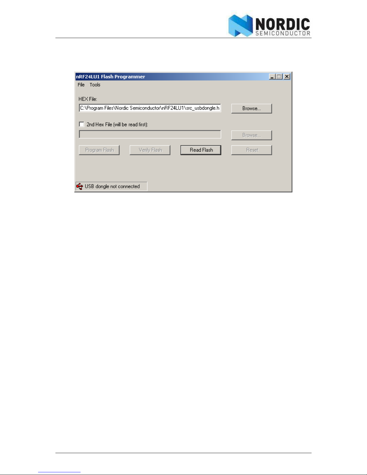
The nRF24LU1 Flash Programmer program must then be installed on the PC. When the program is
started, the following screen will appear:
Figure 7 - nRF24LU1 Flash Programmer
When the ISP Dongle is connected to the USB port, the text “USB Dongle not connected” will change
to “USB Dongle connected” and the USB symbol will turn green.
Choose the .HEX file with the “Browse” button and press “Program Flash”. A blue progress bar will
appear. The FLASH is first programmed and then verified. A box will appear if the verification fails.
Page 13

nRF24LU1 Reference Design User Guide
Revision 1.0 Page 13 of 15
7 Configuration and evaluation suite
The nRF24LU1 USB dongle is configured with the configuration and evaluation suite (CES.) The use
of this is described in detail in the nRF24LU1 Development Kit User Guide available on the CD.
Page 14

nRF24LU1 Reference Design User Guide
Revision 1.0 Page 14 of 15
APPENDIX 1: PCB layout
Top silkscreen
Bottom Silkscreen
Top signal layer
Inner layer 1
Inner layer 2
Bottom signal layer
Figure 8 - nRF24LU1 USB Dongle layout
Page 15
nRF24LU1 Reference Design User Guide
Revision 1.0 Page 15 of 15
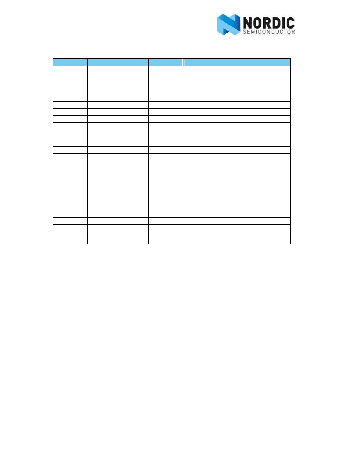
APPENDIX 2: Bill of material
Designator Value Footprint Comment
C1, C2 22pF 0402 NP0 +/-2%
C3 2.2nF 0402 X7R +/-10%
C4 4.7pF 0402 NP0 +/-2%
C5, C6 1.0pF 0402 NP0 +/-2%
C7, C8 10nF 0402 X7R +/-10%
C9, C10 33nF 0402 X7R +/-10%
C11 100n 0402 X7R +/-10%
C12 10uF 0603 X5R +/-20%. 6.3v
C13 2.2pF 0402 NP0 +/-2%
C14 22pF NP0 +/-2%
C15 NA
J1 Molex 48037 USD SMD USB Type A
J2 JST BM05B-SRSS-TB SH-5 1mm connector SH-series
L1 5.6nH 0402 Chip Inductor +/-5%, Murata LQP15-series
L2, L3 6.8nH 0402 Chip Inductor +/-5%, Murata LQP15-series
L4 3.9nH 0402 Chip Inductor +/-5%, Murata LQP15-series
R1 1M 0402 5%
R2 22k 0402 1%
R3, R4 22R 0402 5%
R6, R8 10k 0402 5%
R7 10R 0402 5%
U1 nRF24LU1 QFN32L/5x5 Nordic Semiconductor
X1 16MHz XTAL 2520
Epson Toyocom FA-20H 16MHz, CL=12pF,
+/-20ppm
PCB 0004KJO
Table 1 - nRF24LU1 USB Dongle Bill of Material.
 Loading...