

Norco SOMB-073 User Manual
SOMB-073
QSEVEN Carrier Board
User Manual V1.0

Content
Chapter 1 Product Introduction......................................................................................................1
1.1 Product Specification........................................................................................................1
Chapter 2 Interface Instruction......................................................................................................3
2.1 Interface Location and Dimension Diagram....................................................................3
2.2 Jumper Setting..................................................................................................................3
2.2.1 Start Upon Power-on Hardware Switch(JAT)......................................................4
2.2.2 COM2 Jumper Setting(J5, J6, J7) ....................................................................4
2.2.3 LVDS Voltage Jumper Setting(JLVDS) .............................................................5
2.3 Interface Specification......................................................................................................6
2.3.1 SATA Interfaces(SATA1, SATA2, JSATA) .........................................................6
2.3.2 Serial Ports(COM1,COM2) ...............................................................................8
2.3.3 Display Interface(VGA, LVDS) ........................................................................10
2.3.4 LVDS Backlight Control(JLVDS) .....................................................................11
2.3.5 USB Ports(USB, USB45) ................................................................................12
2.3.6 Network Interface(LAN)...................................................................................13
2.3.7 Keyboard and Mouse Connector(PS2) ..........................................................13
2.3.8 Audio Interface (AUDIO)......................................................................................15
2.3.9 GPIO Connector(JGP) ....................................................................................15
2.3.10 Power Interface(DC_JACK)............................................................................17
2.3.11 Front Panel Connector(JFP) .........................................................................17
2.3.12 SD Card Socket..................................................................................................19
2.3.13 PCIE_X1 Port.....................................................................................................19
2.3.14 MiniPCIE Port(MINI_PCIE).............................................................................19

Chapter 1. Product
Introduction

SOMB-073 QSEVEN Carrier Board
1
Chapter 1 Product Introduction
1.1 Product Specification
Standard Structure
●QSEVEN Carrier Board
●Conforms to MINI-ITX specification with a dimension of 170mm×170mm
Storage
●2* standard SATA interfaces
●1*SDIO port compatible with MMC
Display Interface
●1*standard DB15 VGA port with resolution up to 1280×1024@85Hz
●1*2×10Pin supporting 24/18bit LVDS interface with resolution up to 1280×768@60Hz
I/0
●Adopt Winbond W83627DHG-P I/O chip
●2*COM with COM1 supporting RS232 and COM2 supporting RS-232/422/485
●1set standard double layer PS2 KB&MS connector
●1*2×5Pin,8Bits GPIO port
USB
●6*USB2.0
●2 group double layer standard USB port
●1*2x5Pin interface, able to converted to 2*standard USB ports
LAN
●Adopt RTL8211CL+RTL8111D chip
●2*standard RJ45 ports
Audio Interface
●Adopt ALC887 chip
●Standard tri-layer AUDIO interface supporting MIC-IN, LINE-IN, LINE-OUT

SOMB-073 QSEVEN Carrier Board
2
Expansions
●1*PCIE_×1
●1*MINI-PCIE
Power Supply
●+12V Single Power Supply
Environment
●Operating Temperature:
-40℃-80℃(Industrial grade)
0℃-60℃(commercial grade)
●Storage Temperature: -40℃-85℃
●Operating Humidity: 0-95% relative humidity, no-condensing
Chapter 2. In
terface
Instruction
SOMB-073 QSEVEN Carrier Board
3
Chapter 2 Interface Instruction
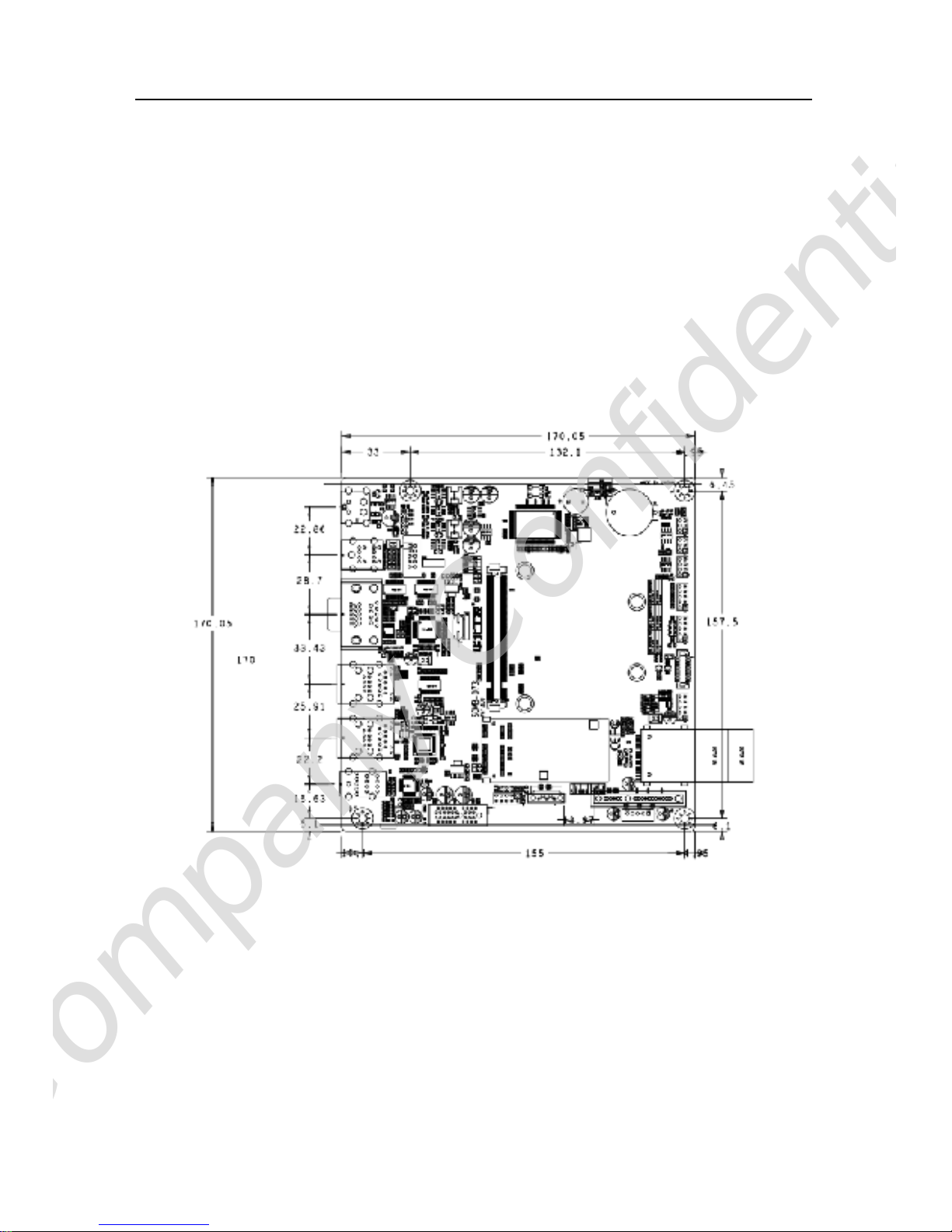
2.1 Interface Location and Dimension Diagram
The following picture is the interface index for SOMB-073. When you install this device, please
consult it and read the following instruction. During the installation, please care for some
devices, as the improper installation of some components will lead to system failure.
Remark: During installation, in order to protect the parts of motherboard, please wear your
antistatic gloves.
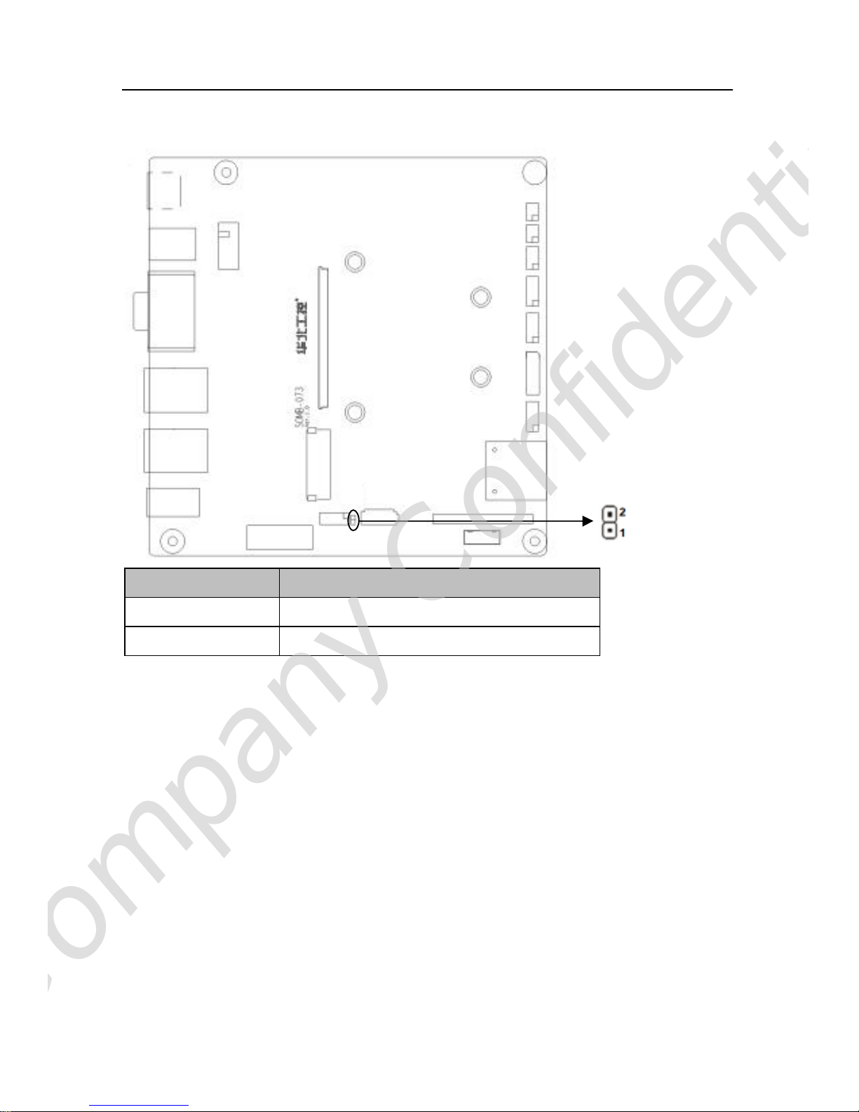
2.2 Jumper Setting
Please config the jumpers accordingly before installing hardware devices
Note: How to identify jumper and PIN1 of interface
Please observe the word mark of plug socket, it will use “1” or bold line or triangular symbols;
and please look at the back of PCB,each of interface weld spot has a squar point, that is PIN 1;
The pin1 of all jumpers will have a white arrow.
SOMB-073 QSEVEN Carrier Board
4
2.2.1 Start Upon Power-on Hardware Switch(JAT)
JAT Power Mode
Close Self-start upon power on
Open Non self-start upon power on
2.2.2 COM2 Jumper Setting(J5, J6, J7)
J5,J6,J7 are used to config the transmission mode of COM2. COM2 supports
RS232/RS422/RS485. Users can config this port based on the actual needs.
 Loading...