

Page 1
NORCAL 2N2/XX V1.2
Assembly Manual
Copyright 2008/2009 by
Jim Kortge, K8IQY
and NORCAL
1
Page 2

Introduction
This is the assembly manual for the NORCAL 2N2/XX transceiver designed by Jim Kortge, K8IQY.
A great deal of effort has gone into the design of the rig and this manual to assure that the kit you are
about to build will work properly. This is not a beginning builders kit. It has a great many parts (over
300) and assumes the builder has some working knowledge of electronics and electronic parts. To
successfully build this transceiver, one needs to be able to understand and follow a schematic diagram,
convert resistor and molded inductor value call outs to the equivalent color code, and be able to
recognize various capacitor types. In addition, one needs to be able to read and understand this manual,
follow the instructions correctly, and work carefully.
A common assembly manual is used for all 2N2/XX rigs, therefore, no parts values are given in this
manual, only part designators. This assembly manual is used with the band specific Bill of Material
(BOM) and schematic diagram to identify the part values being installed. The schematic diagram for
each band contains the actual part value for each designator. Using this approach encourages the
builder to become familiar with the schematic diagram of the 2N2/XX transceiver being built so that
he/she is familiar with the design of the rig should any troubleshooting be necessary. However, if all of
the parts are installed in their correct locations, the rig will perform as designed and no troubleshooting
will be required!
With that thought in mind, go slowly and double check your work to avoid having to remove either an
incorrect part or a correct part installed in the wrong location on the PC board (PCB). As a
suggestion, make a 2X size copy of the schematic diagram. While you are building, check off the parts
installed in the brackets [ ] provided in this manual, while also highlighting the part on the schematic as
a cross check. When you are done building, all of the parts shown on the schematic should be
highlighted. (On 40-meters, the Receive RF Amplifier stage is not built, so those parts will not be
highlighted.)
A parts overlay page is included in the Appendix. This page will show how the various transformers
and trimmer capacitors are to be mounted. An “F” designates the “flat side” of a trimmer capacitor
(TCx designation). When mounting a wound transformer, the primary (“Pri” notation) is always the
winding with the most turns. The secondary (“Sec” notation) is the winding with the fewer or equal
number of turns, if the transformer is a bifilar type. Transformer T5 is somewhat unique, as it has two
secondaries, a 3-turn and a 1-turn. The primary is connected to the locations marked “P” as shown on
the overlay, the 3-turn secondary to “S1” on the overlay, and the 1-turn secondary to “S2” on the
overlay. All transformers having several turns for the primary and fewer turns for the secondary can be
wound with the secondary interleaved between the primary winding turns from approximately centered
on the primary winding to near the end where its leads will be soldered to the appropriate pads on the
PCB. The location is not critical. An examination of the various figures supplied will illustrate this
approach.
This manual is structured to build a section and then test it to assure it is working correctly, before
moving on. Space is also provided at the end of each test section to write down your measurements and
observations. You are encouraged to do this as it will help later on if you run into problems or need
assistance. Using this approach promotes confidence the end product will work, since all of the
previous stages worked. If you build a section and it doesn't work properly, do not continue on,
2
Page 3
expecting that the section will fix itself. It will not and the remainder of the build will be
compromised. Please fix any and all problems as they occur!
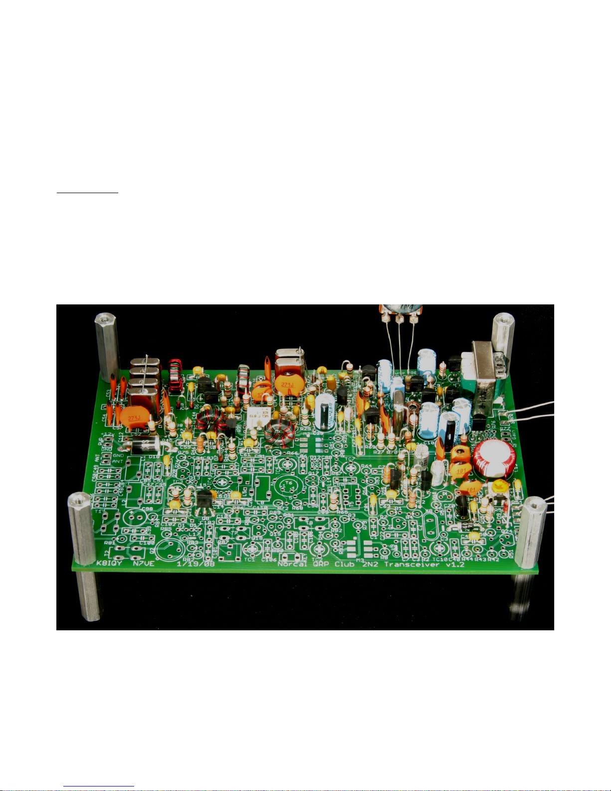
PCB Preparation
[ ] Assemble the four 1-inch hex screws and 1-inch hex nuts to the four corners of the PCB. The
screws go on the bottom side and the nuts on the top side. This hardware holds the PCB up off
the work surface and makes it easy to work on regardless of which side is up.
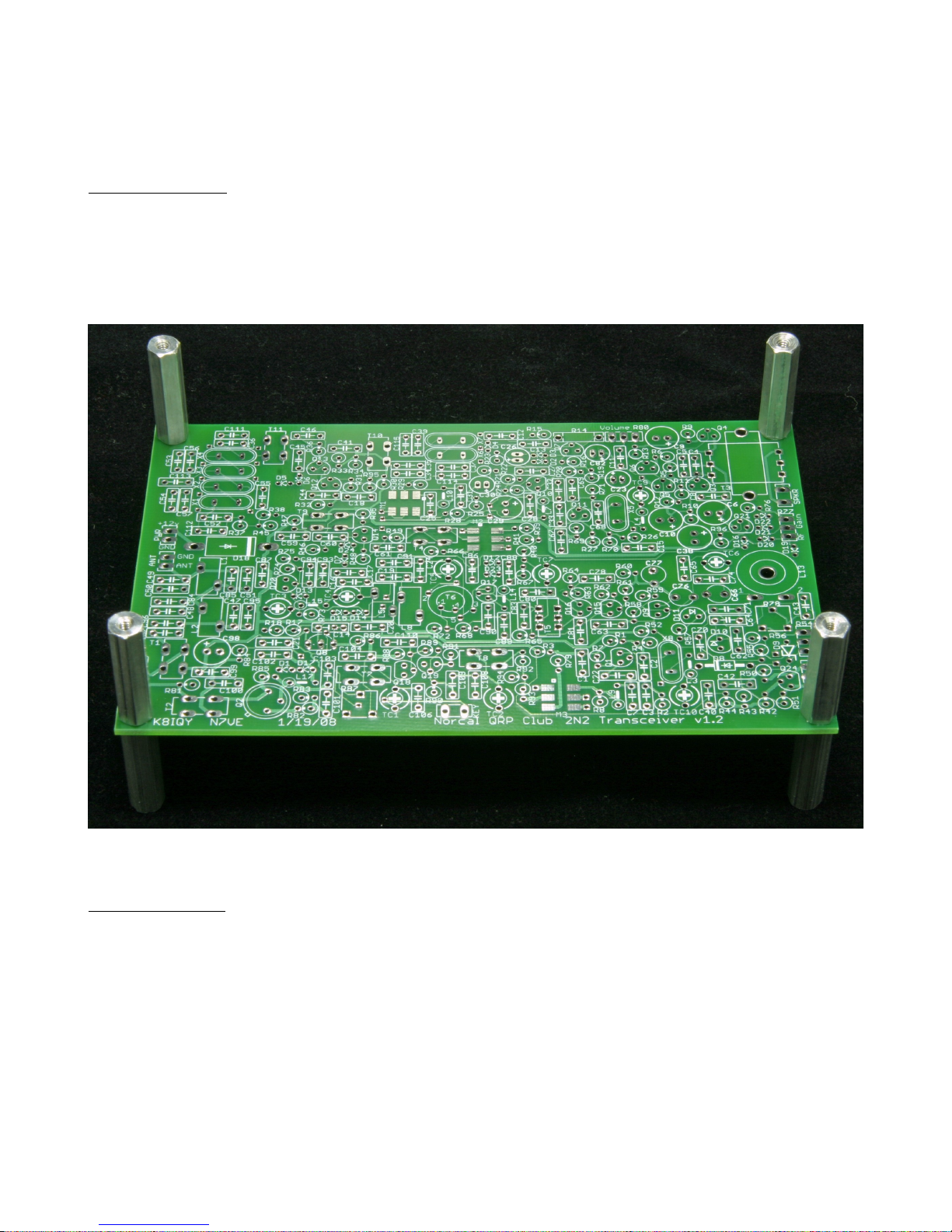
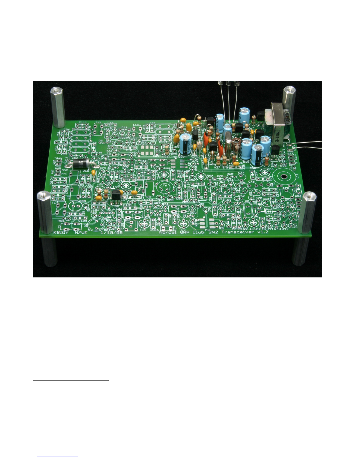
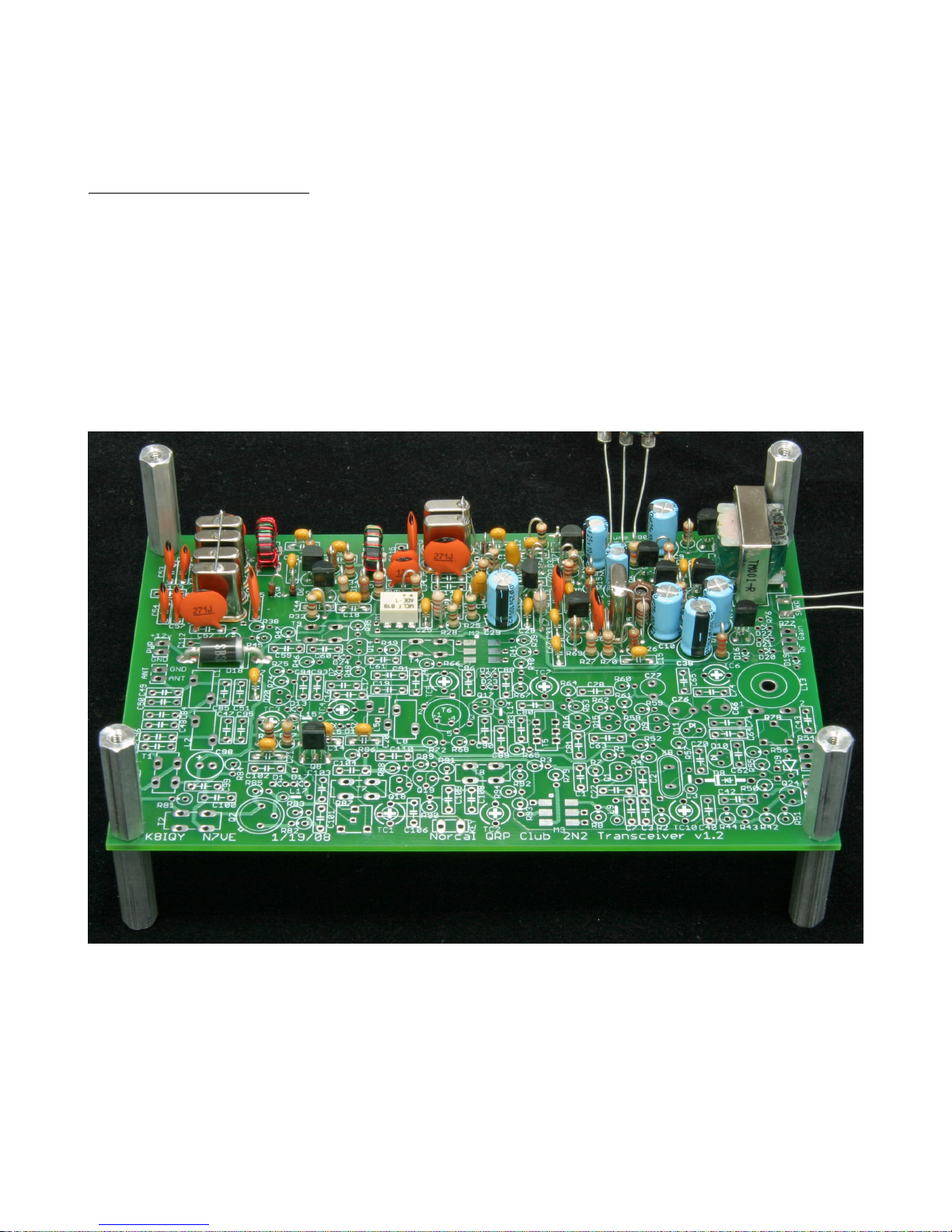
Your PCB should look like that shown in the figure.
Power protection
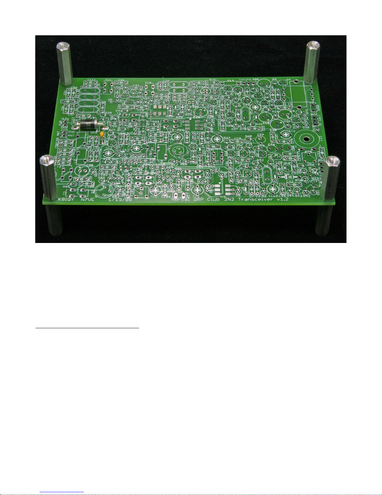
[ ] Install diode D18
[ ] Install capacitor C87.
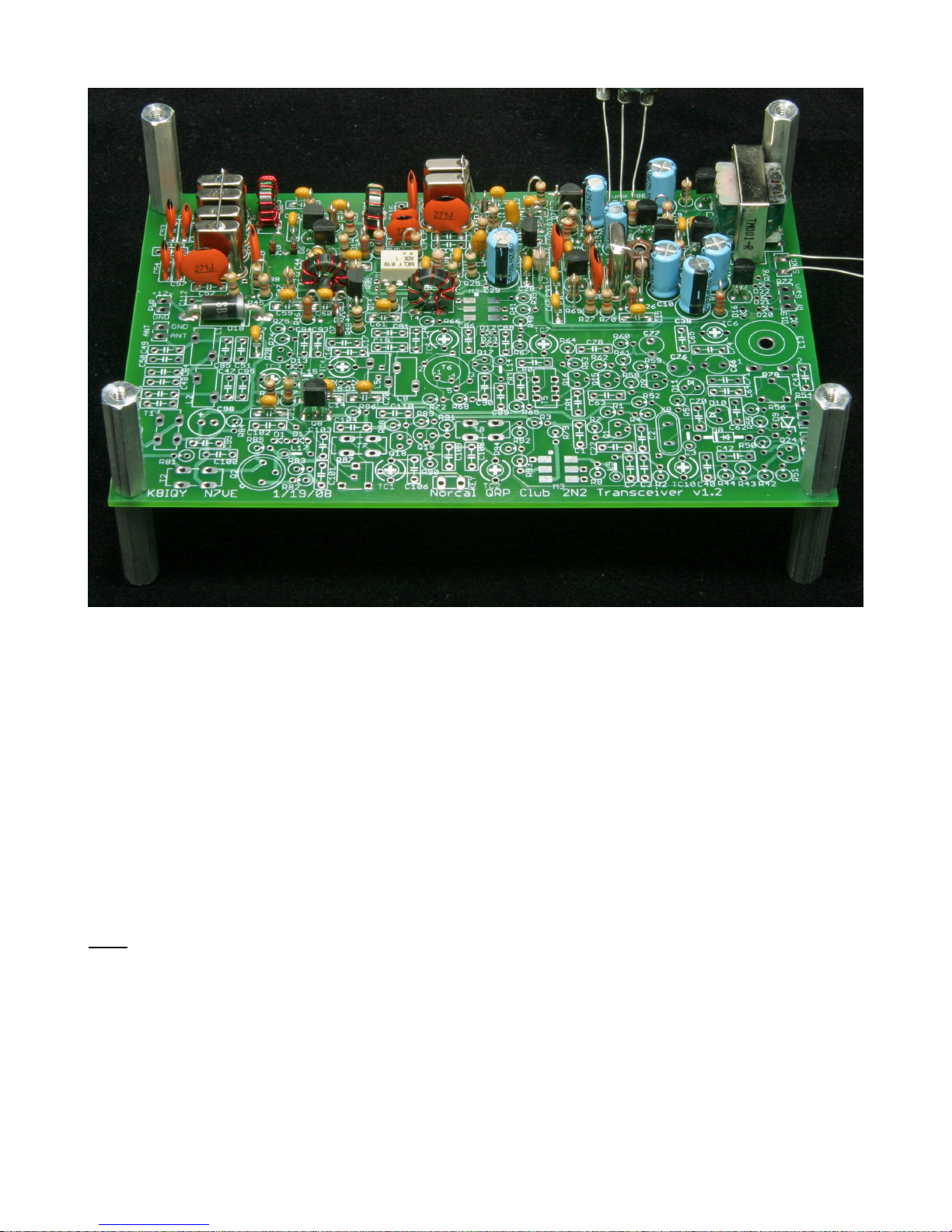
Your PCB should look like that shown in the next figure.
- Figure 1 -
3
Page 4
- Figure 2 -
Test - Apply 12 volts to the board. With a DVM or VOM, measure that more than 11.7 volts
appears at the junction of D18 and C87.
Your Measurements/Observations - ______________________________________________
____________________________________________________________________________
Receive Active Power Decoupler
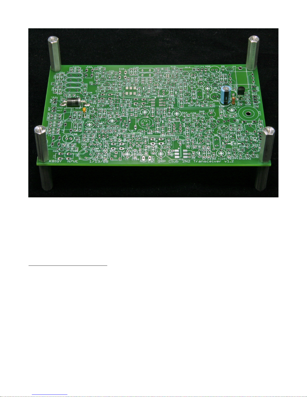
[ ] Install transistor Q21
[ ] Install resistor R96
[ ] Install capacitor C38 matching the polarity markings on the capacitor case with those on the
PCB.
Your PCB should look like that shown in the next figure.
4
Page 5
- Figure 3 -
Test – Apply 12 volts to the board. Measure with a DVM or VOM that 11.5 volts (or more)
appears at the left center pad where transformer T3 will be installed.
Your Measurements/Observations - ______________________________________________
____________________________________________________________________________
Receive Main Audio Amplifier
[ ] Install transformer T3; note orientation, “P” side toward the interior of the PC board. There is
no need to solder the mounting tabs; doing so makes it virtually impossible to remove the
transformer should it be mounted incorrectly.
[ ] Install transistors Q3, Q4, Q5 and Q6.
[ ] Install resistors R5, R6, R9, R10, R11, R12 and R13.
[ ] Install capacitors C4, C5, C8 and C11.
[ ] Install electrolytic capacitors C6, C9, C10 and C82 matching the polarity markings on the case
with those on the PCB.
5
Page 6
[ ] Install volume control R80 (marked A10K) to the pads marked “VOLUME” using discarded
leads from previously installed components as shown in the next figure.
- Figure 4 -
[ ] Install the SPKR jack, using the rear terminals, to the pads marked “SPKR” using discarded
leads from previously installed components as was done above. Other controls will be installed
on a temporary basis similar to these two elements. Once the rig is completed and working,
these parts will be removed and rewired when the PCB and controls are installed in the case.
Your PCB should look like that shown in the next figure.
Test – Connect a speaker or headphones to the “SPKR” jack. Apply power to the board. Rotate
the volume control fully clockwise and touch the center pad of the pad set marked “VOLUME”;
- Figure 5 -
6
Page 7
60 Hz hum should be heard coming from the speaker or headphones.
Your Measurements/Observations - ______________________________________________
____________________________________________________________________________
Receive/Transmit Keying
[ ] Install the PN2907A PNP transistor at Q8
[ ] Install resistors R17 and R18
[ ] Install capacitors C14, C20 and C21
Your PCB should look like that shown in the next figure.
Test – Apply 12 volts to the board. Confirm with a DVM or VOM that at least 11.5 volts (+V
Tx) appears at the collector of Q8 (left pad of R86 location) when the “KEY” pads are
connected together.
- Figure 6 -
7
Page 8
Your Measurements/Observations - ______________________________________________
____________________________________________________________________________
Receive Mute
[ ] Install the J176 JFET at Q7
[ ] Install diodes D2, D3, and D4. Note cathode ends (bar) so they are installed correctly. The
anode of D3 and the cathode of D2 should be the non-grounded ends.
[ ] Install the two test points provided for the R14 location, then install R14. Using these test
points allows R14 to be easily removed and replaced should the audio level during transmit
not be set to your liking.
[ ] Install resistors R15 and R16.
[ ] Install capacitors C12 and C13.
Your PCB should look like that shown in the next figure.
- Figure 7 -
8
Page 9

Test – Connect a speaker or headphones to the “SPKR” jack. Apply power to the board.
Advance the volume control to maximum. Touch the top (ungrounded end) of diode D2; 60 Hz
hum should be heard coming from the speaker or headphones. Rotate volume control R80
counter clock wise (CCW) to verify the hum level changes. At full volume, jumper the pads
marked “KEY” and verify that the 60 Hz hum is muted.
Your Measurements/Observations - ______________________________________________
____________________________________________________________________________
Receive Audio Preamplifier
[ ] Install transistor Q10.
[ ] Install resistors R19, R20, R21, R22, R23 and R24.
[ ] Install capacitors C27 and C28.
[ ] Install tantalum (tan color, both leads on one end) capacitors C26 and C30 matching the polarity
markings on the case with those on the PCB.
[ ] Install electrolytic capacitors C23 and C29 matching the polarity markings on the case with
those on the PCB.
Your PCB should look like that shown in the next figure.
9
Page 10
- Figure 8 -
Test – Connect a speaker or headphones to the “SPKR” jack. Apply power to the board. Touch
the pad on the minus end of tantalum capacitor C30 or the lower pad for L10. The hum volume
should be louder than it was before this stage was added.
Your Measurements/Observations - ______________________________________________
____________________________________________________________________________
Receive Local Oscillator (RxLO)
[ ] Install inductors L4 and L7.
[ ] Install trimmer capacitor TC9. The rounded end is the grounded end.
[ ] Install transistor Q11.
[ ] Install resistors R26, R27, R28, R69, R70 and R71.
[ ] Install capacitors C15, C32, C33, C67, C68 and C69.
[ ] Install crystal X5; it will be one of two marked LO or XX. Place a spacer (made from brown
10
Page 11
bag paper) over the crystal leads before soldering it to the PCB or leave a small space between
the case and the PCB. This will keep the crystal case from shorting out PCB traces. Ground the
crystal case with a short piece of wire to the provided adjacent ground pad.
Your PCB should look like that shown in the next figure.
- Figure 9 -
Test – Apply power to the board. Measure the LO output at the top of resistor R28 with a
suitable device. Either an oscilloscope or RF Probe with readout device can be used. The
output should be at least 1.8 volts peak-to-peak, or 0.60 volts RMS when measured on an
oscilloscope and 0.7 volts peak when measured using a typical passive RF probe connected to a
DVM.
Your Measurements/Observations - ______________________________________________
____________________________________________________________________________
Receive Product Detector
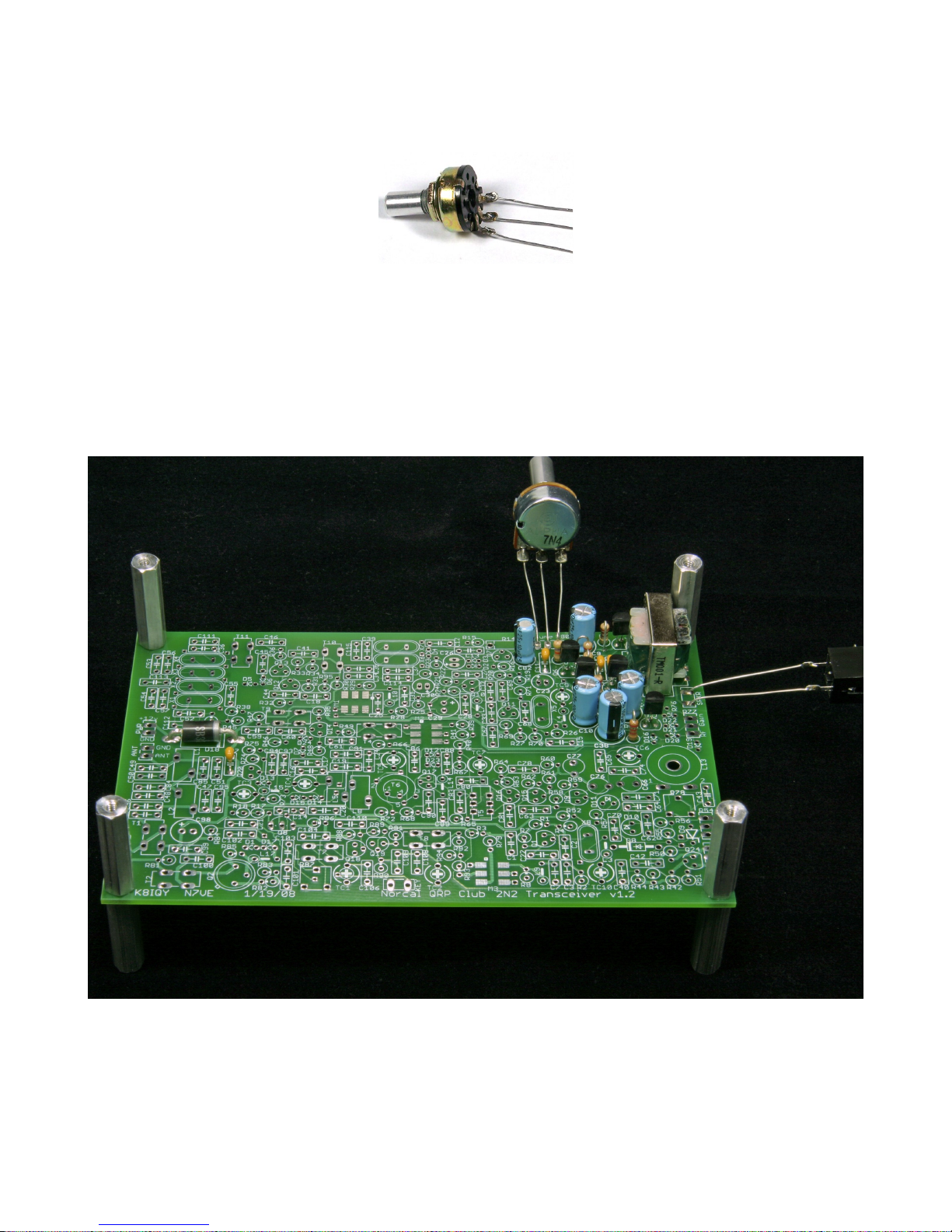
[ ] Install mixer M1. A black dot on the part and a white dot on the PCB denote the location of
Pin 1. Solder the pin 1 lead only. Reconfirm this part is oriented correctly before soldering the
remaining leads.
11
Page 12
[ ] Install resistor R25.
[ ] Install capacitors C25 and C31.
[ ] Install molded inductor L10.
Your PCB should look like that shown in the next figure.
Test – Connect a speaker or headphones to the “SPKR” jack. Apply power to the board.
Measure the mixer drive at the top of resistor R28. It should now show an output level of
at least 0.60 volts peak-to-peak, or 0.27 volts RMS when measured on an oscilloscope and 0.2
volts peak when measured using a typical passive RF probe connected to a DVM. Connecting
an antenna to pin 3 of mixer M1 or the left pad for C37 should provide atmospheric noise
(static) at the audio output.
Your Measurements/Observations - ______________________________________________
____________________________________________________________________________
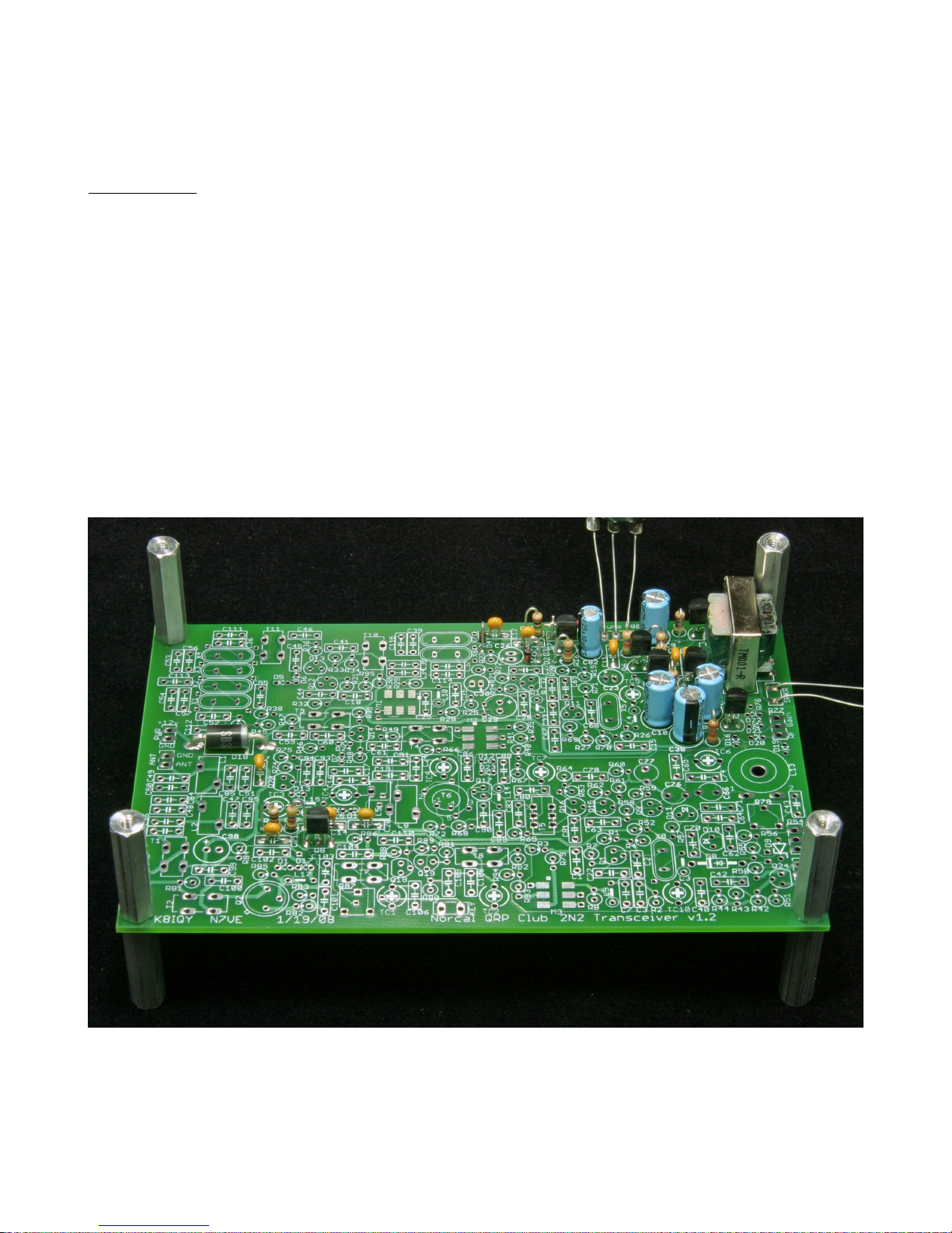
Receive Post IF Amplifier Crystal Filter
[ ] Install resistor R29.
- Figure 10 -
12
Page 13
[ ] Install capacitor pairs C37/C114, C34/C35, and C39/C115. Some of these capacitors may not be
used at the IF frequency employed in your rig. Unused capacitors are shown on the schematic
with a value of 0 pF.
[ ] Install crystals X6 and X7. Place a spacer (made from brown bag paper) over the crystal leads
before soldering it to the PCB or leave a small space between the case and the PCB. This will
keep the crystal case from shorting out PCB traces. Ground each crystal case with a short piece
of wire to the provided adjacent ground pad.
Your PCB should look like that shown in the next figure.
Test – Connect a speaker or headphones to the “SPKR” jack. Apply power to the board.
Connect an antenna to the output side of capacitor C39. Listen to the restricted noise
bandwidth due to the crystal filter. If doing this test in the evening, you may be able to hear a
shortwave broadcast station on the IF frequency of your rig.
Your Measurements/Observations - ______________________________________________
____________________________________________________________________________
- Figure 11 -
13
Page 14
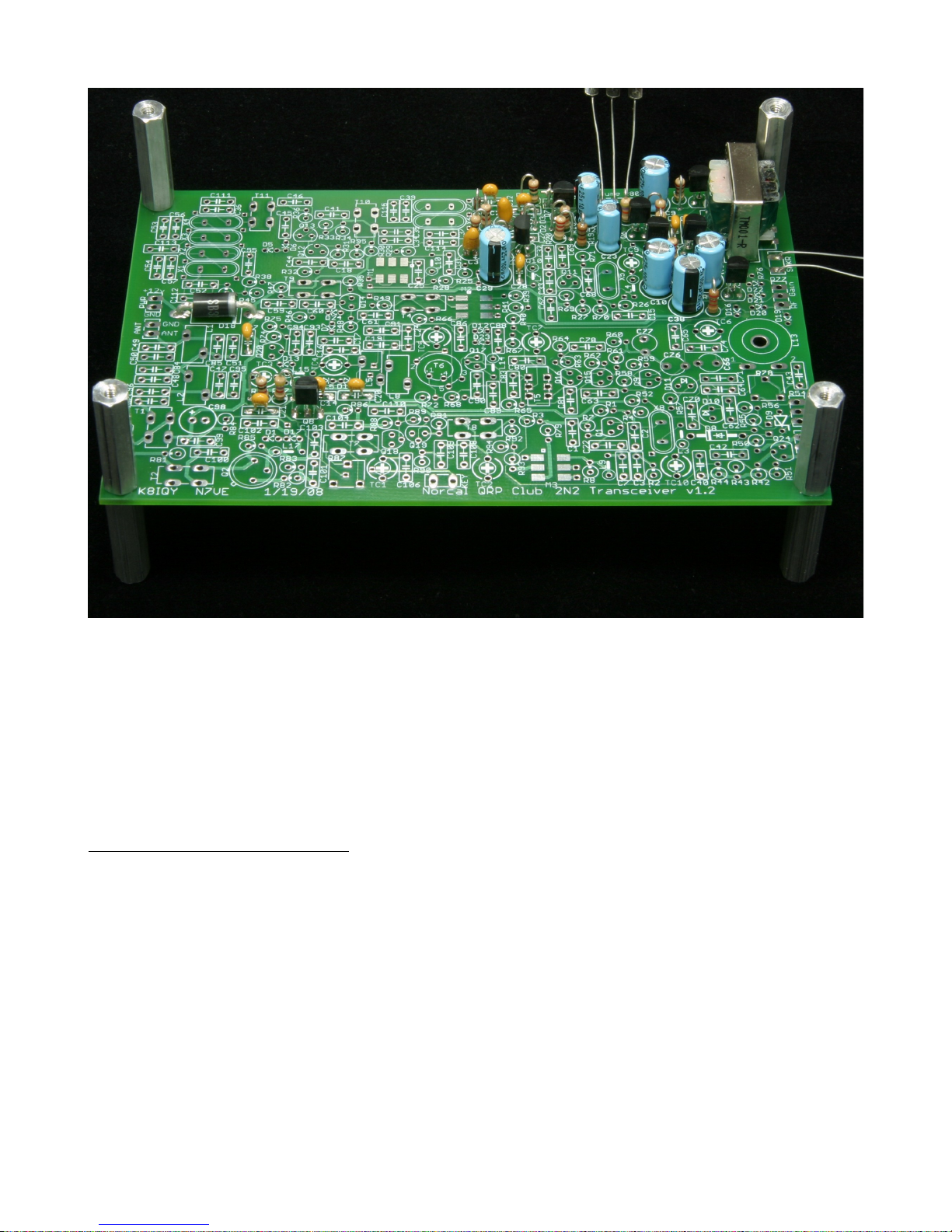
Receive IF Amplifier
[ ] Wind and install transformers T10 and T11. Each time a wire passes through the center of the
toroid, it is counted as 1-turn.
[ ] Install the MPSH10 transistors at Q12 and Q13. These devices look similar to several of the
other plastic encased transistors. Make sure the correct pair is selected.
[ ] Install diodes D5 and D6. Make sure the cathode ends (bar) are oriented correctly.
[ ] Install resistors R30, R31, R32, R33, R34, R36, and R95.
[ ] Install capacitors C18, C41, C44, C45, and C46.
Your PCB should look like that shown in the next figure.
Test - Connect a speaker or headphones to the “SPKR” jack. Apply power to the board.
Connect an antenna to the primary side of transformer T11 or to the right pad where C36 will
be installed. You should hear band noise, mostly static, at a very loud level.
- Figure 12 -
14
Page 15
Your Measurements/Observations - ______________________________________________
____________________________________________________________________________
Receive Main Crystal Filter
[ ] Install capacitor pairs C36/C111, C53/C56, C55/C113, C54/C57 and C52/C112. Some of these
capacitors may not be used at the IF frequency employed in your rig. Unused capacitors are
shown on the schematic with a value of 0 pF.
[ ] Install crystals X1, X2, X3, and X4. Place a spacer (made from brown bag paper) over the
crystal leads before soldering it to the PCB or leave a small space between the case and the
PCB. This will keep the crystal case from shorting out PCB traces. Ground the case of each
crystal with a short piece of wire to the provided, adjacent ground pads.
Your PCB should look like that shown in the next figure.
Test - Connect a speaker or headphones to the “SPKR” jack. Apply power to the board.
Connect an antenna to the right pad of C52 or to the upper pad where R37 will be installed. You
should hear band noise, mostly static, at a loud level and very restricted in bandwidth due
to the action of this crystal filter.
- Figure 13 -
15
Page 16
Your Measurements/Observations - ______________________________________________
____________________________________________________________________________
Receive Post-Mixer Amplifier
[ ] Wind and install transformers T4 and T9. T4 can be wound with either a pair of wires twisted
together at 8-10 turns per inch and then wound on the core, or with the pair of wires wound in
parallel. Either method will yield a suitable transformer. An example of each method is shown
in the next figures.
- Figure 14 - - Figure 15 -
[ ] Install transistor Q14.
[ ] Install diodes D7 and D24. Note cathode ends (bar) so they are installed correctly.
[ ] Install resistors R35, R37, R38, R45, R46, R47, R48 and R49.
[ ] Install capacitors C59, C60 and C61.
Your PCB should look like that shown in the next figure.
16
Page 17
- Figure 16 -
Test - Connect a speaker or headphones to the “SPKR” jack. Apply power to the board.
Connect an antenna to the upper-right pad of T4 or the pin 2 pad of where mixer M2 will be
installed. You should hear band noise, mostly static, at a very loud level and very restricted in
bandwidth due to the action of the crystal filters. As you are listening, rotate trim capacitor to
change the LO frequency being injected into mixer M1. Starting with the capacitor at minimum
capacitance, (the highest sounding static) rotate this trimmer until the lowest sounding static
occurs. This adjustment will be used to optimize the LO injection point to center the received
signal in the middle of the main crystal filter in the final receiver alignment.
Your Measurements/Observations - ______________________________________________
____________________________________________________________________________
VFO
[ ] Wind and install inductor L13. Use the supplied shouldered nylon washers on either side of
toroid and the nylon screw and nut to secure it to the PCB. Tighten until the wound toroid is
snug, but do not over tighten and strip the screw threads. Cut off excess screw material
protruding through the nut.
[ ] Install trim capacitor (orange color) TC6.
17
Page 18
[ ] Install Q9
[ ] Install diodes D8, D9 and D10. Note cathode ends (bar) on D8 and D9 so they are installed
correctly. D10 (a MV1662) looks like a transistor with only two leads and has no markings on
it, just colored bands.
[ ] Install resistors R52, R55, R56, R58, R59 and R60.
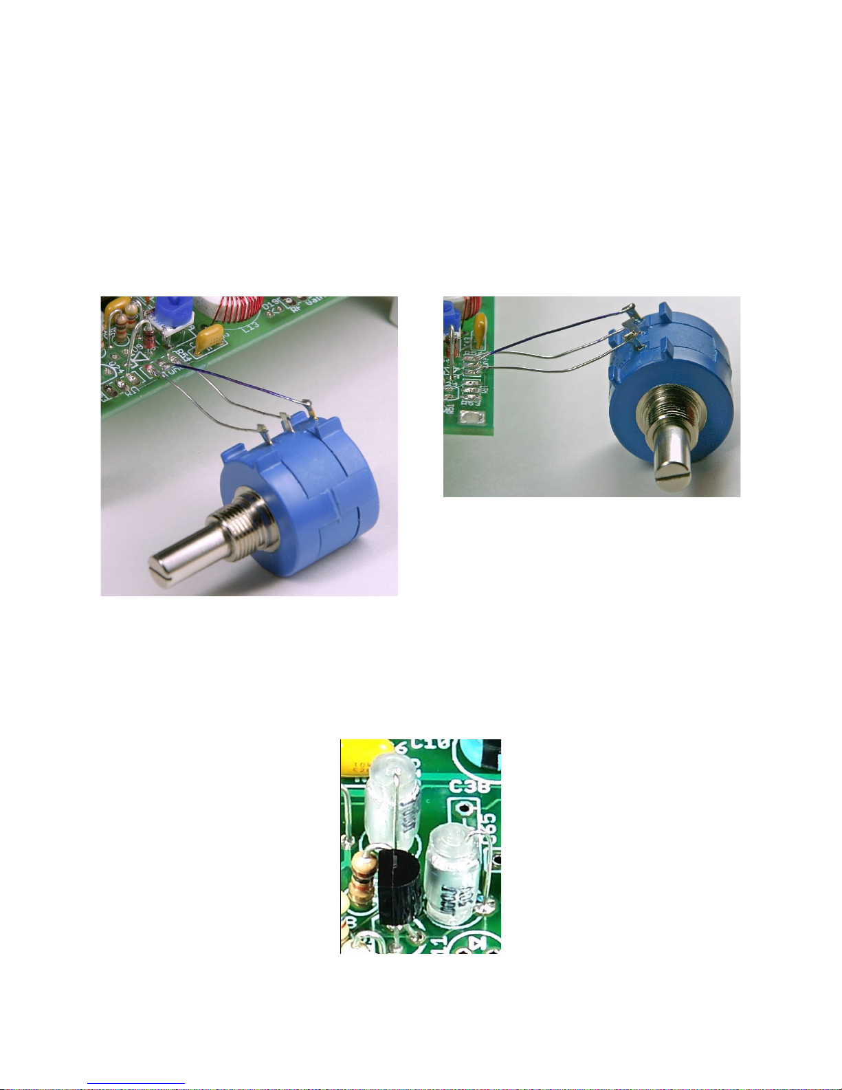
[ ] Install trim potentiometer R78 and control potentiometer R54. R54 is wired using leads from
previously installed components and oriented so that when wired to the PCB, the terminals are
pointing as shown in the next figures.
- Figure 17a - - Figure 17b -
[ ] Install polystyrene capacitors C76, and C77. This set of capacitors is mounted “on end”
as shown in the next figure.
- Figure 18 -
18
Page 19

[ ] Install capacitors C42, C43, C62, C63, C64, C65, C66 and C74.
Your PCB should look like that shown in the next figure.
- Figure 19 -
Test – Apply power to the PCB. Connect an RF probe or oscilloscope to the top of resistor R60.
The RF probe should show an output level of approximately 0.16 volts. On an oscilloscope, the
waveform should approximately match that shown in the next figure.
- Figure 20 -
If a frequency counter is available, connect it to the top of R60 and measure the frequency. The
19
Page 20
displayed frequency will change with the rotation of R54, the tuning potentiometer. The high
frequency end of the VFO tuning range is set by trim capacitor TC6 and the low frequency end
by trim resistor R78. Adding in the RIT circuitry (in a later step) will change the tuning range
and span of the VFO.
Your Measurements/Observations - ______________________________________________
____________________________________________________________________________
VFO Buffer
[ ] Install Q15
[ ] Install resistors R61, R62, and R65.
[ ] Install capacitor C81.
Your PCB should look like that shown in the next figure.
Test – Apply power to the PCB. Connect an RF probe or oscilloscope to the top of resistor R62.
- Figure 21 -
20
Page 21

The RF probe should show an output level of approximately 0.15 volts. On an oscilloscope, the
waveform should approximately match that shown in the next figure.
- Figure 22 Your Measurements/Observations - ______________________________________________
____________________________________________________________________________
VFO Driver
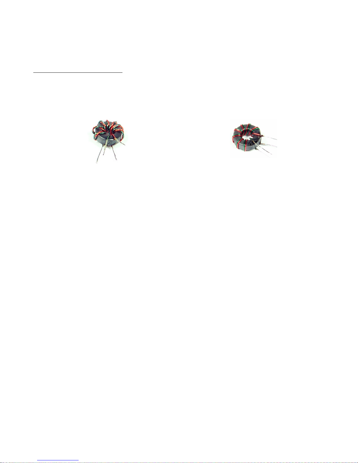
[ ] Wind transformer T5. Put the 16-turn primary (use red wire, not green wire as shown) and the
3-turn secondary (use green wire, not red as shown) windings on the T37-61 dull gray core
with green dot, as shown in the next figure.
- Figure 23 -
Install it onto the PCB. After it is secured, add the remaining 1-turn secondary winding. When
installed, the toroid will look like that in the next figure.
21
Page 22

- Figure 24 -
[ ] Install trim capacitor TC7.
[ ] Install transistor Q16.
[ ] Install resistors R39, R40, R41, R63, and R64.
[ ] Install capacitors C78, C80, and C83.
Your PCB should look like that shown in the next figure.
- Figure 25 -
22
Page 23

Test – Temporarily connect a 51 Ohm resistor from the top of resistor R40 to ground. This
resistor supplies a load for the VFO driver stage. Apply power to the PCB. Connect an RF
probe or oscilloscope to the top of resistor R40. Peak the driver tuned circuit by rotating TC7
while watching the output level. At the peak setting, the RF probe should show an output level
of approximately 0.9 volts. On an oscilloscope, the waveform should approximately match
that shown in the next figure.
- Figure 26 -
Your Measurements/Observations - ______________________________________________
____________________________________________________________________________
Receive Main Mixer
[ ] Install mixer M2. Before soldering all of the leads, make sure it it oriented correctly. A dot on
the part and on the PCB denote the location of Pin 1.
[ ] Install resistor R66.
Your PCB should look like that shown in the next figure.
23
Page 24

- Figure 27 -
Test – Connect a speaker or headphones to the “SPKR” jack. Apply power to the PCB. Connect
an RF probe or oscilloscope to the top of resistor R39. The RF probe should show an output
level of approximately 0.25 volts. On the oscilloscope, the waveform should approximately
match that shown in the next figure.
- Figure 28 -
24
Page 25

Connect an antenna to the top of resistor R66. Band noise and maybe a station can be heard.
Adjust LO trim capacitor TC9 until the received band noise sounds the loudest and is at
approximately 1 KHz. This isn't a critical adjustment at this time, just use your ears and let
them be your guide. The receiver is listening to signals in the band and at the image frequency,
so you may hear CW and shortwave broadcast signals together.
Your Measurements/Observations - ______________________________________________
____________________________________________________________________________
Receive RF Amplifier
[ ] The Receive RF Amplifier stage is not used on 40-meters. Instead, a jumper is connected
between the upper pad for capacitor C86 and transformer pad T6-5. 40-Meter builders can
proceed directly to the “Receive Input Band Pass Filter” section.
[ ] Wind and install transformer T6. The finished transformer should look like the next figure
with a 3-turn winding, a tap, and then followed with a 5-turn winding.
- Figure 29 -
The 1-turn emitter winding is added after the transformer is soldered on to the PCB. On 30-
meters, this transformer has a 2-turn winding, a tap, and a 1-turn winding.
[ ] Install inductor L14.
[ ] Install transistor Q17.
[ ] Install diodes D12 and D23. Note cathode ends (bar) so they are installed correctly.
[ ] Install resistors R67, R68, and R72.
[ ] Install capacitors C86, C88, C89, and C90.
Your PCB should look like that shown in the next figure.
25
Page 26

- Figure 30 -
Test – Connect a speaker or headphones to the “SPKR” jack. Apply power to the PCB.
Connect an antenna through a 0.1uF capacitor to the upper pad where trim capacitor TC5
will be mounted. The band noise and stations heard should be louder than in the previous step
due to the gain of this stage.
Your Measurements/Observations - ______________________________________________
____________________________________________________________________________
Receive Input Band Pass Filter
[ ] Wind and install inductors L5 and L8.
[ ] Install trim capacitors TC4 and TC5.
[ ] Install capacitors C16, C17, C19, C24, and C91.
Your PCB should look like that shown in the next figure.
26
Page 27

- Figure 31 -
Test – Connect a speaker or headphones to the “SPKR” jack. Apply power to the PCB.
Connect an antenna to the right pad where inductor L15 will be mounted. Alternately peak
trim capacitors TC4 and TC5 until the band noise is the loudest. Only stations in the band
should now be heard.
Your Measurements/Observations - ______________________________________________
____________________________________________________________________________
Receive RF Gain and RF Mute
[ ] Install inductor L15.
[ ] Install trim capacitor TC3.
[ ] Install the 2N4124 NPN transistor at Q20. Make sure this is the correct transistor.
[ ] Install diodes D13, D14, D15, D16, D19, D20, D21, and D22. Note cathode ends (bar) so they
are installed correctly.
[ ] Install resistors R73, R74, R75, and R76.
27
Page 28

[ ] Install RF gain control R77 to the pads marked “RF Gain” using discarded leads from
previously installed components
[ ] Install capacitors C93 and C94.
Your PCB should look like that shown in the next figure.
- Figure 32 -
Test – Connect a speaker or headphones to the “SPKR” jack. Apply power to the PCB.
Connect an antenna to the lower pad where capacitor C95 will be mounted. Alternately peak
trim capacitors TC3, TC4 and TC5 until the band noise or a received signal is the loudest.
Adjust R77 to verify the RF gain can be reduced.
Your Measurements/Observations - ______________________________________________
____________________________________________________________________________
Receive Incremental Tuning (RIT)
[ ] Install the 2N7000 MOSFET at Q24.
[ ] Install diode D11. This diode (a MV209) looks like a transistor with markings on it but with
only two leads.
[ ] Install resistors R42, R43, R44, R50, R51 and R57.
[ ] Install RIT control R53 to the pads marked “RIT” using discarded leads from previously
installed components
[ ] Install capacitors C40, C70, and C71.
28
Page 29

Your PCB should look like that shown in the next figure.
- Figure 33 -
Test – Connect a speaker or headphones to the “SPKR” jack. Apply power to the PCB.
Connect an antenna to the lower pad where capacitor C95 will be mounted. Adjust R53 in both
directions to verify the receiver tuning changes approximately 3 KHz up and down in
frequency from the center detent position.
Your Measurements/Observations - ______________________________________________
____________________________________________________________________________
At this stage of the assembly, the receive strip is complete and fully functional. You might want to
readjust the RxLO (trim capacitor TC9) to set the injection point so that cw stations are at a
pleasing note, around 700 Hz, and the loudest you can make them. As you adjust the RxLO,
you'll have to re-tune the station with tuning potentiometer R54 to keep it centered in the
passband of the receiver.
Transmit Local Oscillator (TxLO)
[ ] Install inductors L3 and L9.
[ ] Install trim capacitor TC10. The rounded end is the grounded end.
[ ] Install transistor Q1.
[ ] Install resistors R1, R2, R3, R4, R7 and R8.
[ ] Install capacitors C1, C2, C3, C7 and C22.
29
Page 30

[ ] Install crystal X8; it will be the last one marked LO or XX. Place a spacer over the crystal leads
before soldering it to the PCB. Ground the crystal case with a short piece of wire to the
provided adjacent ground pad.
Your PCB should look like that shown in the next figure.
- Figure 34 -
Test – Apply power to the board. Measure the TxLO output at the top of resistor R8 with a
suitable device. Either an oscilloscope or RF Probe with readout device can be used.. Jumper
the “Key” pads together to key the transmitter. The RF probe should show an output level of
approximately 0.7 volts. On the oscilloscope, the waveform should approximately match that
shown in the next figure.
- Figure 35 -
30
Page 31

Your Measurements/Observations - ______________________________________________
____________________________________________________________________________
Transmit Main Mixer
[ ] Install mixer M3. Before soldering all of the leads, make sure it it oriented correctly. A dot on
the part and on the PCB denote the location of Pin 1.
[ ] Install resistor R79.
Your PCB should look like that shown in the next figure.
- Figure 36 -
Test – Connect a speaker or headphones to the “SPKR” jack. Apply power to the PCB. Connect
an RF probe or oscilloscope to the top of resistor R8. Jumper the “Key” pads together to key the
transmitter. The RF probe should show an output level of approximately 0.2 volts. On the
oscilloscope, the waveform should approximately match that shown in the next figure.
31
Page 32

- Figure 37 Connect an RF probe or oscilloscope to the top of resistor R79. The RF probe should show an
output level of approximately 0.13 volts. On the oscilloscope, the waveform should
approximately match that shown in the next figure.
- Figure 38 -
Adjust trim capacitor TC10 so that a cw tone can be heard from the receive strip.
Your Measurements/Observations - ______________________________________________
____________________________________________________________________________
Transmit Cascode Amplifier
[ ] Wind and install transformers T7 and T8.
[ ] Install trim capacitors TC1 and TC2.
[ ] Install transistors Q18 and Q19.
32
Page 33

[ ] Install resistors R86, R88, R89, R90, R91, R92, R93, and R94
[ ] Install trim potentiometer R87.
[ ] Install capacitors C104, C106, C108, C109, and C110.
Your PCB should look like that shown in the next figure.
- Figure 39 -
Test – Connect a speaker or headphones to the “SPKR” jack. Apply power to the PCB. Connect
an RF probe or oscilloscope to the top pad of capacitor C103. Adjust trim resistor R87 CW to
the end of its travel. Jumper the “Key” pads together to key the transmitter. Alternately adjust
trim capacitors TC1 and TC2 for maximum output. The RF probe should show an output level
of approximately 1 volt. On the oscilloscope, the waveform should approximately match that
shown in the next figure.
33
Page 34

- Figure 40 -
Your Measurements/Observations - ______________________________________________
____________________________________________________________________________
Transmit Driver Amplifier
[ ] Wind and install transformer T2.
[ ] Install inductor L17.
[ ] Install the 2N2219A transistor at Q2. Make sure that the bottom of the case is not tight to the
PCB; space it up about 1/32nd of an inch.
[ ] Install diodes D1 and D17.
[ ] Install resistors R81, R82, R83, R84, and R85.
[ ] Install capacitors C100, C101, C102 and C103.
Your PCB should look like that shown in the next figure.
34
Page 35

- Figure 41 -
Test – Connect a speaker or headphones to the “SPKR” jack. Apply power to the PCB. Connect
an RF probe or oscilloscope to the top of resistor R81. Adjust trim resistor R87 to the middle of
its travel. Jumper the “Key” pads together to key the transmitter. Alternately adjust trim
capacitors TC1 and TC2 for maximum output. The RF probe should show an output level
of approximately 1.7 volts. On the oscilloscope, the waveform should approximately match that
shown in the next figure.
Your Measurements/Observations - ______________________________________________
____________________________________________________________________________
Transmit Final Amplifier
- Figure 42 -
35
Page 36

[ ] Wind and install transformer T1. This transformer can be wound with either a pair of wires
twisted together at 8-10 turns per inch and then wound on the core, or with the pair of wires
wound in parallel. Either method will yield a suitable transformer. An example of each method
was shown earlier in this manual.
[ ] Install the 2SC5739 transistor at Q25. Make sure the longer side of the TO-220 case is toward
the outside edge of the PCB before soldering the leads.
[ ] Install capacitors C96, C97 and C99.
[ ] Install electrolytic capacitor C98 matching the polarity markings on the case with those on the
PCB.
Your PCB should look like that shown in the next figure.
Test – No test will be performed at this step because we do not have a load on the final
amplifier. We will add the output low pass filter in the next step and then test the final amplifier
with a resistive dummy load attached to absorb the RF output power.
Transmit Output Low Pass Filter
[ ] Wind and install inductors L1 and L2.
[ ] Install capacitor pairs C47/C95, C48/C84, C51/C85, and C49/C50. Some of these capacitors
may not be used in your rig, depending on the band it is on. Unused capacitors are shown on
the schematic with a value of 0 pF.
[ ] Install the BNC output connector to the pads marked “ANT” using discarded leads from
- Figure 43 -
36
Page 37

previously installed components. The center of the BNC is wired to the “ANT” pad and the
BNC ground to the “GND” pad.
Your PCB should look like that shown in the next figure.
- Figure 44 -
Test – Attach a TO-220 style heat sink (or fabricate something similar) to final transistor Q25 as
shown in the next figure.
- Figure 45 -
Connect a speaker or headphones to the “SPKR” jack. Connect a 50 Ohm dummy load/watt
meter to the output BNC connector. Connect an RF probe or oscilloscope to the “ANT” side of
the BNC connector and the ground of the probe or scope to the “GND” side of the BNC
connector. Adjust trim resistor R87 fully counter clockwise. Apply power to the PCB. Jumper
the “Key” pads together to key the transmitter. Do not keep the transmitter keyed for more
than 30 seconds at a time while performing these tests, to prevent the final transistor from
overheating. Begin turning R87 in a clockwise direction while alternately adjusting trim
37
Page 38

capacitors TC1 and TC2 for maximum output. Keep turning R87 until an output level of 4watts is obtained. The receiver should be hearing the transmitted signal. The RF probe should
show an output level of approximately 16 volts under these conditions. On the oscilloscope, the
waveform should approximately match that shown in the next figure.
- Figure 46 -
Your Measurements/Observations - ______________________________________________
____________________________________________________________________________
Final Adjustments
Now that the construction of your 2N2/XX PCB is complete, we can go back and do some final tuneup work to optimize the performance of the rig. We'll do it once here and again after the rig is installed
in the case.
VFO
This step sets up the VFO to 100 KHz of band coverage (50 KHz for 30 Meters) and sets the low end
of the VFO to match the low end of the band. This calibration step requires either a frequency counter
or another receiver capable of receiving the VFO across its tuning range.
[ ] Connect a speaker or headphones to the “SPKR” jack. Apply power to the PCB. Connect the
frequency counter probe to the top of resistor R40. Let the rig and the counter warm up for ½
hour before proceeding. If using another receiver for this calibration, turn it on and let it also
warm up.
[ ] Center the RIT potentiometer, R53. Adjust trim potentiometer R78 fully counter clockwise.
Turn the VFO frequency 10-turn potentiometer fully clockwise. Adjust trim capacitor TC6 so
that the upper VFO frequency matches the frequency shown in the table on page 56 for the band
your rig is on. A frequency tolerance of +/- 200 Hz is close enough.
[ ] Turn the VFO frequency 10-turn potentiometer fully counter clockwise. Adjust trim
potentiometer R78 until the lower VFO frequency matches the frequency shown in the page 56
38
Page 39

table for the band your rig is on. A frequency tolerance of +/- 200 Hz is close enough.
[ ] Since there is some interaction between these two settings, repeat these two adjustments until
both ends of the band are set to your satisfaction.
Receiver Front-End
This procedure will optimize the receive sensitivity. With the receiver operating, apply a mid-band
signal to the antenna connector using a signal generator (the NORCAL S1-S9 generator is
recommended) set for 50 uV or less. As an alternate, attach an antenna and find a moderately strong
signal. The VFO should be tuned to the center the signal in the receive passband. Beginning with trim
capacitor TC3, peak TC3, TC4, and TC5. Repeat this step a few times to obtain the loudest signal
under these contitions. Reduce the signal level to approximately 1 uV and repeat the peaking process.
TxLO
In this step, we will match the transmit frequency to the received frequency With the rig transmitting
into a dummy load, adjust the transmit LO trim capacitor, TC10, to match the tone that is heard in the
receiver when a cw signal is being received.
Transmit Strip
This step will maximize the RF power output from the rig.
[ ] Set the VFO to the middle of its tuning range, 5-turns from full CCW on potentiometer R54.
[ ] With the rig transmitting into a dummy load/watt meter, peak the power output by adjusting
trim capacitor TC7 in the VFO driver stage.
[ ] Alternately adjust trim capacitors TC1 and TC2 in the Cascode Amplifier stage for maximum
power output as indicated on the watt meter.
[ ] Adjust trim resistor R87 in the Tx Driver stage to set the power output level you want.
[ ] Alternate between the previous two steps until you are satisfied with the settings.
[ ] Adjust the RF output power with trim resistor R87 to the desired power level. Four-watts is
recommended.
Remove PCB Temporary Wiring
This step will remove the external controls and their temporary wiring.
[ ] With the completed PCB still on the standoffs, carefully remove all of the external controls and
their wiring. It is suggested that all wires between a control and the PCB be cut in the middle.
[ ] With the PCB inverted, so that the bottom side is up, heat a connection point and pull the
wire out from the top side, the side facing the workbench surface.
[ ] Using a solder sucker, carefully reheat that pad and suck the solder out so that the hole is open.
39
Page 40

[ ] Repeat the process for all of the pads that still have wires soldered to them until the board is free
of wires and all holes are open.
Your PCB should look like that shown in the next figure. (Ignore the fact that the Key pad holes
still contain solder – it was a slight oversight by the author. :-o)
- Figure 47 -
Final PCB Wiring
This step will add the wires to the PCB that connect to the external controls.
[ ] RIT (R53) - Cut 8 1/2 inch pieces of wire in colors Red, White, and Green. Strip 1/8 inch of
insulation from each end and carefully tin. Solder the Red wire to the RIT left pad, the White
wire to the RIT center pad, and the Green wire to the RIT right pad.
Your PCB should look like that shown in the next figure.
40
Page 41

- Figure 48 -
[ ] TUNE (R54) - Cut 7 inch pieces of wire in colors Red, White, and Green. Strip 1/8 inch of
insulation from each end and carefully tin. Solder the Red wire to the TUNE left pad, the White
wire to the TUNE center pad, and the Green wire to the TUNE right pad.
Your PCB should look like that shown in the next figure.
[ ] RF Gain (R77) - Cut 4 1/2 inch pieces of wire in colors White, Green, and Black. Strip 1/8 inch
of insulation from each end and carefully tin. Solder the White wire to the RF Gain left pad, the
Green wire to the RF Gain center pad, and the Black wire to the RF Gain right pad.
Your PCB should look like that shown in the next figure.
- Figure 49 -
41
Page 42

- Figure 50 -
[ ] SPKR (Speaker) - Cut 4 inch pieces of wire in colors White and Green. Strip 1/8 inch of
insulation from each end and carefully tin. Solder the White wire to the SPKR left pad and the
Green wire to the SPKR right pad.
Your PCB should look like that shown in the next figure.
[ ] Volume (R80) - Cut 1 1/2 inch pieces of wire in colors White, Green, and Black. Strip 1/8 inch
of insulation from each end and carefully tin. Solder the Black wire to the Volume left pad, the
Green wire to the Volume center pad, and the White wire to the Volume right pad as viewed
from the closest PCB edge.
Your PCB should look like that shown in the next figure.
- Figure 51 -
42
Page 43

- Figure 52 -
[ ] PWR (+12/GND) - Cut 4 1/2 inch pieces of wire in colors Red and Black. Strip 1/8 inch of
insulation from each end and carefully tin. Solder the Red wire to the PWR left pad and the
Black wire to the PWR right pad as viewed from the closest PCB edge.
Your PCB should look like that shown in the next figure.
[ ] ANT (ANR/GND) - Cut a 3 1/2 inch piece of RG-174 coaxial cable. Strip 5/16 inch of outer
insulation from each end. Carefully unbraid the outer shield using a pointed tool such as a scribe
and twist the strands tightly. Carefully tin the first 1/16 inch of the shield on either end. Strip
1/8 inch of insulation from the inner conductor on each end and carefully tin. Solder the outer
shield to the ANT left pad and the inner conductor to the ANT right pad as viewed from
the closest PCB edge.
Your PCB should look like that shown in the next figure.
- Figure 53 -
43
Page 44

- Figure 54 -
[ ] KEY (Key/Gnd) - Cut 2 inch pieces of wire in colors White and Black. Strip 1/8 inch of
insulation from each end and carefully tin. Solder the Black wire to the KEY left pad and the
White wire to the KEY right pad as viewed from the closest PCB edge.
Your PCB should look like that shown in the next figure.
- Figure 55 -
Once all of the wires are installed on the PCB, it should look like that shown in the next figure.
44
Page 45

- Figure 56 -
Set the wired PCB aside for the moment while the case components are assembled.
Case Component Assembly
The case is comprised of a bottom shell, top shell, front panel, and rear panel. The top and bottom
shells are held together by a plastic latch system, allowing the top shell to be easily removed for access
to the inside of the 2N2/XX rig. The front and rear panels contain all of the controls and connectors for
the rig. Pem nuts are used to hold the PCB in the bottom shell and the front and rear panels to the
bottom shell.
The case components are shown in this collection of photos.
- Figure 57 -
- Figure 58 -
45
Page 46

- Figure 59 - - Figure 60 -
[ ] Using 2-56 X 5/16 flat head screws, #2 internal tooth lock washers, and 2-56 hex nuts,
secure the tab part of the latch assembly to each side of the top shell. The tab goes on
the outside and with the protrusion on the tab extending beyond the top shell edge
as shown in the detailed photo.
- Figure 61 -
[ ] Using 2-56 X 5/16 flat head screws, #2 internal tooth lock washers, and 2-56 hex nuts,
secure the latch part of the latch assembly to each side of the bottom shell as shown in the
photo.
- Figure 62 -
46
Page 47

[ ] With the latch components installed on the bottom and top shell pieces, place the top on the
bottom and test the latches to assure they are working properly. The next photo shows how the
case will look if the latches are installed correctly.
- Figure 63 -
Put the completed case aside for now. It will be used again shortly, but next, the front panel will receive
its controls and then be wired to the PCB. After that, the PCB will be installed in the case and the front
panel screwed into place.
Front Panel Assembly
In the next steps, the controls for the front panel will be installed, the front panel controls wired, and
the PCB and front panel installed into the bottom shell.
[ ] Before the Volume control (R80-marked as A10K) and RF Gain control (R77-marked as A1K)
potentiometers are installed into the front panel, their shafts need to be shortened by 7/32 inch. Mark
the shaft on each, hold the shaft in a vise, and cut the shaft to length with a fine-tooth hack saw. After
making the cut, clean up the end of the shaft with a small mill file.
The next photo shows a modified potentiometer (lower) compared to one that is unaltered (upper).
47
Page 48

- Figure 64 -
[ ] Install Volume control potentiometer R80 (marked A10K) into the front panel from the back
side, put on the washer, and then the hex nut. Tighten the control finger tight, as it needs to be
able to rotate for ease of wiring later on.
[ ] Repeat the above process with RF Gain control potentiometer R77 (marked A1K)
[ ] Repeat the above process with RIT control potentiometer R53 (marked B1K)
[ ] Install the 10-turn Tuning potentiometer R54 by putting the internal tooth lock washer on the
shaft, inserting into the panel from the back side, and then adding the hex nut on the panel front
side . As before, tighten only finger tight so that the control can be rotated for ease of wiring.
The front panel should look like the next two photos.
Front View Rear View
- Figure 65 - - Figure 66 -
Front Panel Wiring
In the next steps, the front panel will be wired to the PCB.
[ ] With the PCB and front panel laying face down and aligned side to side with the PCB, begin by
soldering the wires from the Volume pads to the Volume control potentiometer. Use a pair of
the small supplied knobs under the top edge of the front panel to stabilize it. The Volume
48
Page 49

control potentiometer should be rotated so that the wires reach it equally. Use the photographs
as a reference in soldering the correctly colored wire to each potentiometer terminal.
- Figure 67 -
[ ] Next, solder the wires from the RF Gain pads to the RF Gain control potentiometer. Use the
photograph as a reference in soldering the correctly colored wire to each potentiometer
terminal.
- Figure 68 -
[ ] Solder the wires from the Tuning pads to the 10-turn Tuning potentiometer. Use the
photograph as a reference in soldering the correctly colored wire to each potentiometer
terminal.
- Figure 69 -
49
Page 50

[ ] Next, solder the wires from the RIT pads to the RIT control potentiometer. Use the
photograph as a reference in soldering the correctly colored wire to each potentiometer
terminal.
- Figure 70 -
With all of the wire sets correctly soldered to their respective potentiometers, the PCB-Front Panel
assembly should look like the next photo.
[ ] This next step is optional, but one that will improve the assembly appearance of the finished rig.
If done at this stage of the assembly, it will be easier. Using wide waxed nylon dental tape or
preferably lacing cable, do some lacing together of the control wires from the various
potentiometers back to the PCB. The arrangement is not critical, except for the Volume control
potentiometer. The lacing should not include this control as there are audio signals on the wires;
the remaining controls only have DC voltages on them. The next photo shows an example of a
suggested lacing method.
- Figure 71 -
50
Page 51

- Figure 72 -
Installing the PCB and Front Panel into Case Bottom Shell
The next several steps will result in the PCB being mounted to the bottom case shell and the front panel
being screwed into place on the front of the bottom case shell.
[ ] Begin by removing all of the standoffs from the four corners of the PCB
[ ] Using four 4-40 X 5/16 inch pan head screws, #4 internal tooth lock washers, and 1/8 X 3/16
inch spacers, mount the PCB to the bottom of the case. The PCB is oriented such that the final
transistor is on the side of the case bottom where it will be secured in a later step. Place the
spacers on top of the pem nuts, then place the PCB down on the spacers, and carefully insert a
screw with a lock washer through a PCB mounting hole and into the pem nut. Tighten each
screw only finger tight at this point so that small adjustments can still be made.
[ ] Place the 1/8 X 1/2 X 1 inch spacer between the final transistor tab and the case wall. Using a 4-
40 X 1/2 inch flat head screw, #4 internal tooth lock washer, and 4-40 hex nut, secure the final
transistor to the case wall.
[ ] Once the transistor mounting screw is tight, tighten the PCB corner mounting screws. The
assembly should look like the next photo.
51
Page 52

- Figure 73 -
[ ] Using four 4-40 X 1/4 inch flat head screws, mount the front panel to the bottom case shell.
[ ] When the front panel is in place, rotate the potentiometers to optimize the layout of the wiring
going to them. Then, tighten the nuts that hold the potentiometers so that they are snug.
Additional cable lacing can be done at this point to hold the front panel wiring in place. The
assembly should look like the next photos.
Front Panel from Inside Front Panel from Front
- Figure 74 - - Figure 75 -
Rear Panel Assembly
In the section, the rear panel connectors will be installed.
[ ] Install a 1/8 inch stereo jack in the hole marked "Speaker". When viewed from the back side of
the panel, orient the lug on the side of the jack toward the right.
[ ] Install another 1/8 inch stereo jack in the hole marked "Key". When viewed from the back side
of the panel, also orient the lug on the side of this jack toward the right.
52
Page 53

[ ] Install a BNC connector in the hole marked "Antenna". To install this connector, push the
connector through the panel hole, place the wire lug over the back of the connector, put on the
internal tooth lock washer, and follow this with the hex nut. Tighten the assembly with the wire
lug pointing to the left when viewed from the back of the panel. Pry the wire lug up so that it
is oriented at about 60 degrees to the panel surface.
[ ] Finally, install the coaxial power connector in the hole marked "12VDC". The lugs on this
connector should be oriented so that they are left, down, and right when viewed from the back
of the panel.
When all of the connectors are installed, the rear panel should look like the next two photos.
Rear Panel from Rear Rear Panel from Front
- Figure 76 - - Figure 77 -
Installing the Rear Panel into Case Bottom Shell
The next several steps will result in the rear panel being wired and screwed into place on the rear of the
bottom case shell.
[ ] Place the rear panel against the PCB at an angle of about 45 degrees. With the panel held in this
position, tape in place with two strips of masking tape to hold it so that the wires to the rear
panel can be soldered more easily. The next photo shows this setup.
53
Page 54

- Figure 78 -
[ ] Following the details shown in the next photograph, solder the green and white wires coming
from the "SPKR" pads to the "Speaker" stereo connector. The white wire is soldered to the left
lug and the green wire to the right lug as viewed from the front.
[ ] Next, solder the black and white wires coming from the "Key" pads to the "Key" stereo
connector. The white wire is soldered to the left lug and the black wire to the right lug as
viewed from the front.
[ ] Solder the center conductor of the coax coming from the "ANT" pads to the center pin of the
"Antenna" BNC connector. Solder a short length of solid wire (a discarded component lead) to
the ground lug of the BNC connector. Position this wire to be parallel to the coax shield lead
and cut it to an appropriate length so that it overlaps the shield lead. Solder the coax shield lead
and the ground extension lead together.
[ ] Finally, solder the red and black wires coming from the "PWR" pads to the "12VDC" coaxial
power connector. The black lead is soldered to the center lug and the red lead is soldered to the
right lug.
[ ] If you did some lacing of the component leads on the front panel, do the same on the rear panel.
[ ] Remove the masking tape supports. The rear panel should look as shown in the next photo.
54
Page 55

- Figure 79 -
[ ] Screw the rear panel to the case using 4-40 X 1/4 inch flat head screws. As the panel is being
moved into position, route the wires so they are not close to components that have RF signals
on them, such as coils or trimmers, as shown in the next photo.
- Figure 80 -
55
Page 56

Final Assembly
These steps complete the assembly of the 2N2/XX.
[ ] Install small knobs on the RF Gain, Volume, and RIT control potentiometers and the large knob
on the Tuning potentiometer.
[ ] Install the 4 rubber feet on the bottom of the case near the corners.
[ ] Set the case top on the bottom case assembly, engage the latch tabs, and latch the top to the
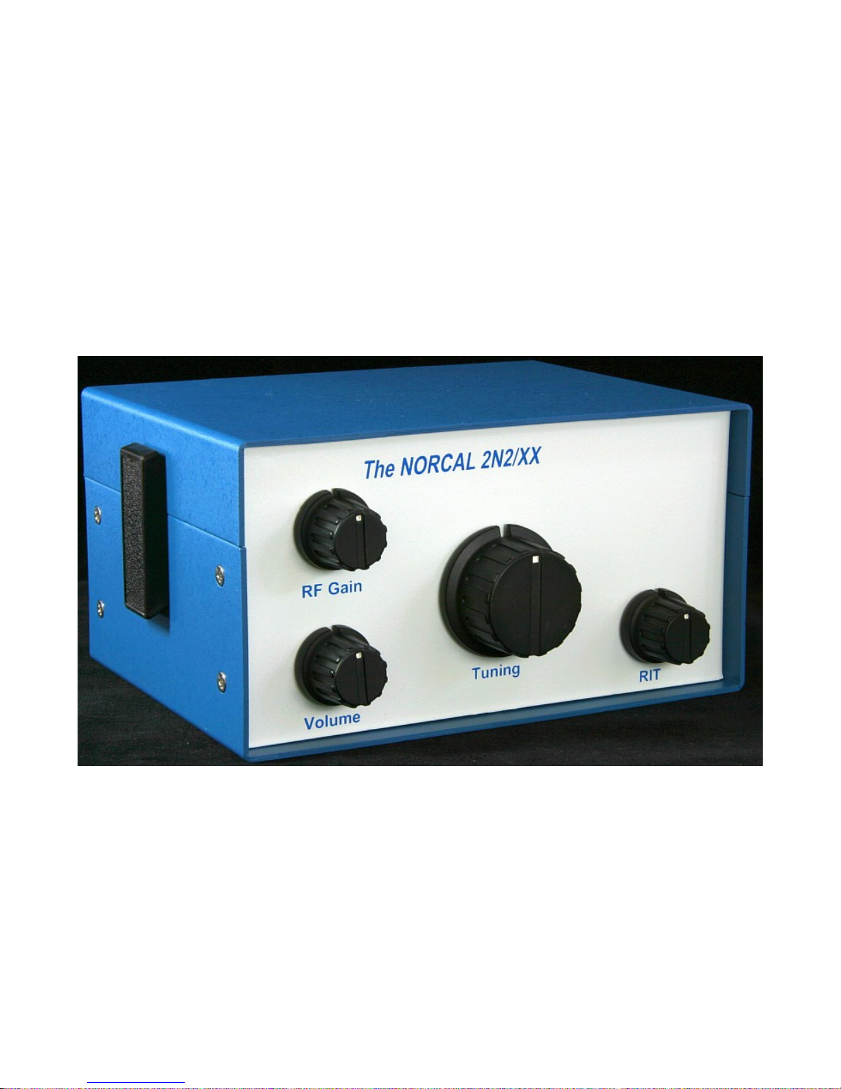
bottom. Your 2N2/XX should look like the one in this last photo!
- Figure 81 -
Congratulation on the successful built of your NORCAL 2N2/XX. We hope you have enjoyed the
building experience, will use the rig often, and enjoy it for many years.
56
Page 57

2N2/XX Appendix
This part of the assembly manual contains specifications, a parts placement diagram, and the schematic
diagrams for each of the available bands. Make sure you are using the correct schematic for the
band you are building. There are significant part value differences among the three bands, therefore,
you must use the correct schematic to successfully complete your 2N2/XX rig.
2N2/XX Features
All discrete component, through-hole (except mixers) design.
Analog through-out; very low noise.
100 KHz band coverage (50 KHz on 30-meters).
10-turn potentiometer for tuning ease.
500 Hz, 6-pole, non-ringing crystal filter.
“Thumpless” QSK keying.
Receiver Incremental Tuning (RIT).
5-watt output on all bands.
2N2/XX Specifications
Sensitivity (MDS): > -120 dBm (-128 dBm on 20 meters, typical).
Opposite Sideband Rejection: > 80 dB.
IF Rejection: > 50 dB.
Image Rejection: > 70 dB.
Intermodulation Dynamic Range (IMDR): > 90 dB.
Input 3rd Order Intercept (IP3): > 8 dB.
Blocking Dynamic Range (BDR): > 105 dB.
Receive current ~ 180 milliamperes.
Transmit current ~ 800 milliamperes (5-watts output).
57
Page 58

Design Tuning Range for Each Band
Band VFO Low VFO High IF Frequency Band Low Band High
20 Meters 3.0000 MHz 3.1000 MHz 11.0000 MHz 14.000 MHz 14.100 MHz
30 Meters 2.7272 MHz 2.7772 MHz 7.3728 MHz 10.100 MHz 10.150 MHz
40 Meters 2.0848 MHz 2.1848 MHz 4.9152 MHz 7.000 MHz 7.100 MHz
The above chart shows the nominal VFO tuning ranges and IF frequencies for each band. However, the
IF filter passband center in the 2N2/XX rigs actually fall just a bit higher than the IF frequencies
shown, typically 500 to 600 Hz higher. What that means is that the VFO frequencies shown may have
to be increased by a small amount to achieve the correct band operating frequencies as shown in the
chart.
58
Page 59

PCB Overlay
2N2/XX V1.2
21 Jan 2008
Page 60

60
Page 61

61
Page 62

62
Page 63

63
Page 64

64
Page 65

65
Page 66

2N2/XX Miscellaneous Information
Toroid Cores
Red core = T37-2 (Powdered Iron)
Yellow core = T37-6 (Powdered Iron)
White core (Used for VFO Inductor) = T50-7 (Powdered Iron)
Shiny gray core = FT37-43 (Ferrite)
Dull gray core (marked with green dot) = FT37-61 (Ferrite)
Toroid Winding Wire Supplied
Item Amount
#28 Red 19 Feet
#28 Green 5 Feet
#26 Red 4 Feet
#26 Green 1 Foot
Hookup Wire Supplied
Item Amount
RG174 Coax 6 inches
Black hookup 19 inches
Red hookup 30 inches
Green hookup 38 inches
White hookup 41 inches
All chassis-to-control hookup wire is #24, stranded, PVC insulated.
66
 Loading...