

Page 1

SCt4812ET Optimization/ATP
Manual
Software Release R16.1.x.x
English
Aug 2002
68P09255A57-2
800 and 1900 MHz
CDMA
PRELIMINARY
Page 2

Notice
While reasonable efforts have been made to assure the accuracy of this document, Motorola, Inc. assumes no liability resulting
from any inaccuracies or omissions in this document, or from use of the information obtained herein. The information in this
document has been carefully checked and is believed to be entirely reliable. However, no responsibility is assumed for
inaccuracies or omissions. Motorola, Inc. reserves the right to make changes to any products described herein and reserves the
right to revise this document and to make changes from time to time in content hereof with no obligation to notify any person
of revisions or changes. Motorola, Inc. does not assume any liability arising out of the application or use of any product,
software, or circuit described herein; neither does it convey license under its patent rights or the rights of others.
It is possible that this publication may contain references to, or information about Motorola products (machines and
programs), programming, or services that are not announced in your country. Such references or information must not be
construed to mean that Motorola intends to announce such Motorola products, programming, or services in your country.
Copyrights
This instruction manual, and the Motorola products described in this instruction manual may be, include or describe
copyrighted Motorola material, such as computer programs stored in semiconductor memories or other media. Laws in
the United States and other countries preserve for Motorola certain exclusive rights for copyrighted material, including
the exclusive right to copy, reproduce in any form, distribute and make derivative works of the copyrighted material.
Accordingly, any copyrighted Motorola material contained herein or in the Motorola products described in this
instruction manual may not be copied, reproduced, distributed, merged or modified in any manner without the express
written permission of Motorola. Furthermore, the purchase of Motorola products shall not be deemed to grant either
directly or by implication, estoppel, or otherwise, any license under the copyrights, patents or patent applications of
Motorola, as arises by operation of law in the sale of a product.
Usage and Disclosure Restrictions
License Agreement
The software described in this document is the property of Motorola, Inc. It is furnished by express license agreement
only and may be used only in accordance with the terms of such an agreement.
Copyrighted Materials
Software and documentation are copyrighted materials. Making unauthorized copies is prohibited by law. No part of the
software or documentation may be reproduced, transmitted, transcribed, stored in a retrieval system, or translated into any
language or computer language, in any form or by any means, without prior written permission of Motorola, Inc.
High Risk Activities
Components, units, or third-party products used in the product described herein are NOT fault-tolerant and are NOT
designed, manufactured, or intended for use as on-line control equipment in the following hazardous environments
requiring fail-safe controls: the operation of Nuclear Facilities, Aircraft Navigation or Aircraft Communication Systems,
Air Traffic Control, Life Support, or Weapons Systems (“High Risk Activities”). Motorola and its supplier(s) specifically
disclaim any expressed or implied warranty of fitness for such High Risk Activities.
Trademarks
and Motorola are registered trademarks of Motorola, Inc.
Product and service names profiled herein are trademarks of Motorola, Inc. Other manufacturers’ products or services
profiled herein may be referred to by trademarks of their respective companies.
Copyright
Copyright 2002 Motorola, Inc.
All Rights Reserved
Printed on
Recyclable Paper
SPECIFICATIONS SUBJECT TO CHANGE WITHOUT NOTICE
REV012501
Page 3

SCt4812ET Optimization/ATP
Manual
Table of Contents
.
.
.
Aug 2002
SC4812ET Optimization/ATP Manual Software Release R16.1.x.x
PRELIMINARY
i
Page 4

Table of Contents
68P09255A57-2
Contents
FCC Requirements xviii. . . . . . . . . . . . . . . . . . . . . . . . . . . . . . . . . . . . . . . . . . . . . . . . . . . . . . . . . . . . . . . . . . . . . . . . . .
Content xviii. . . . . . . . . . . . . . . . . . . . . . . . . . . . . . . . . . . . . . . . . . . . . . . . . . . . . . . . . . . . . . . . . . . . . . . . . . . . .
FCC Part 15 Requirements xviii. . . . . . . . . . . . . . . . . . . . . . . . . . . . . . . . . . . . . . . . . . . . . . . . . . . . . . . . . . . .
FCC Part 68 Requirements xix. . . . . . . . . . . . . . . . . . . . . . . . . . . . . . . . . . . . . . . . . . . . . . . . . . . . . . . . . . . .
Foreword xx. . . . . . . . . . . . . . . . . . . . . . . . . . . . . . . . . . . . . . . . . . . . . . . . . . . . . . . . . . . . . . . . . . . . . . . . . . . . . . . . . . .
General Safety xxii. . . . . . . . . . . . . . . . . . . . . . . . . . . . . . . . . . . . . . . . . . . . . . . . . . . . . . . . . . . . . . . . . . . . . . . . . . . . . .
Revision History xxiv. . . . . . . . . . . . . . . . . . . . . . . . . . . . . . . . . . . . . . . . . . . . . . . . . . . . . . . . . . . . . . . . . . . . . . . . . . . . .
Chapter 1 Introduction 1-1. . . . . . . . . . . . . . . . . . . . . . . . . . . . . . . . . . . . . . . . . . . . . . . . . . . .
Introduction 1-2. . . . . . . . . . . . . . . . . . . . . . . . . . . . . . . . . . . . . . . . . . . . . . . . . . . . . . . . . . . . . . . . . . . . . . . . . . . . . . . . .
Scope of This Document 1-2. . . . . . . . . . . . . . . . . . . . . . . . . . . . . . . . . . . . . . . . . . . . . . . . . . . . . . . . . . . . . .
Document Composition 1-2. . . . . . . . . . . . . . . . . . . . . . . . . . . . . . . . . . . . . . . . . . . . . . . . . . . . . . . . . . . . . . .
CDMA LMF Product Description 1-3. . . . . . . . . . . . . . . . . . . . . . . . . . . . . . . . . . . . . . . . . . . . . . . . . . . . . . . .
Online Help 1-3. . . . . . . . . . . . . . . . . . . . . . . . . . . . . . . . . . . . . . . . . . . . . . . . . . . . . . . . . . . . . . . . . . . . . . . . . .
Why Optimize? 1-3. . . . . . . . . . . . . . . . . . . . . . . . . . . . . . . . . . . . . . . . . . . . . . . . . . . . . . . . . . . . . . . . . . . . . .
What Is Optimization? 1-3. . . . . . . . . . . . . . . . . . . . . . . . . . . . . . . . . . . . . . . . . . . . . . . . . . . . . . . . . . . . . . . .
When to Optimize 1-5. . . . . . . . . . . . . . . . . . . . . . . . . . . . . . . . . . . . . . . . . . . . . . . . . . . . . . . . . . . . . . . . . . . .
Documentation 1-6. . . . . . . . . . . . . . . . . . . . . . . . . . . . . . . . . . . . . . . . . . . . . . . . . . . . . . . . . . . . . . . . . . . . . . . . . . . . . .
Site Documents 1-6. . . . . . . . . . . . . . . . . . . . . . . . . . . . . . . . . . . . . . . . . . . . . . . . . . . . . . . . . . . . . . . . . . . . . . . . . . . . .
Product Documentation 1-6. . . . . . . . . . . . . . . . . . . . . . . . . . . . . . . . . . . . . . . . . . . . . . . . . . . . . . . . . . . . . . .
Test Equipment 1-7. . . . . . . . . . . . . . . . . . . . . . . . . . . . . . . . . . . . . . . . . . . . . . . . . . . . . . . . . . . . . . . . . . . . . . . . . . . . .
Overview 1-7. . . . . . . . . . . . . . . . . . . . . . . . . . . . . . . . . . . . . . . . . . . . . . . . . . . . . . . . . . . . . . . . . . . . . . . . . . . .
LMF Hardware Requirements 1-8. . . . . . . . . . . . . . . . . . . . . . . . . . . . . . . . . . . . . . . . . . . . . . . . . . . . . . . . . .
Test Equipment Guidelines 1-8. . . . . . . . . . . . . . . . . . . . . . . . . . . . . . . . . . . . . . . . . . . . . . . . . . . . . . . . . . . .
Test Equipment Calibration 1-8. . . . . . . . . . . . . . . . . . . . . . . . . . . . . . . . . . . . . . . . . . . . . . . . . . . . . . . . . . . .
Test Cable Calibration 1-9. . . . . . . . . . . . . . . . . . . . . . . . . . . . . . . . . . . . . . . . . . . . . . . . . . . . . . . . . . . . . . . .
Equipment Warm-up 1-9. . . . . . . . . . . . . . . . . . . . . . . . . . . . . . . . . . . . . . . . . . . . . . . . . . . . . . . . . . . . . . . . .
Test Equipment List 1-9. . . . . . . . . . . . . . . . . . . . . . . . . . . . . . . . . . . . . . . . . . . . . . . . . . . . . . . . . . . . . . . . . .
Optional Equipment 1-12. . . . . . . . . . . . . . . . . . . . . . . . . . . . . . . . . . . . . . . . . . . . . . . . . . . . . . . . . . . . . . . . . .
Abbreviations and Acronyms 1-13. . . . . . . . . . . . . . . . . . . . . . . . . . . . . . . . . . . . . . . . . . . . . . . . . . . . . . . . . . . . . . . . . .
BTS Overview 1-15. . . . . . . . . . . . . . . . . . . . . . . . . . . . . . . . . . . . . . . . . . . . . . . . . . . . . . . . . . . . . . . . . . . . . . . . . . . . . .
Major Components 1-16. . . . . . . . . . . . . . . . . . . . . . . . . . . . . . . . . . . . . . . . . . . . . . . . . . . . . . . . . . . . . . . . . . .
RF Cabinet Internal FRUs 1-17. . . . . . . . . . . . . . . . . . . . . . . . . . . . . . . . . . . . . . . . . . . . . . . . . . . . . . . . . . . . .
Sector Configuration 1-22. . . . . . . . . . . . . . . . . . . . . . . . . . . . . . . . . . . . . . . . . . . . . . . . . . . . . . . . . . . . . . . . . . . . . . . . .
Power Cabinet 1-25. . . . . . . . . . . . . . . . . . . . . . . . . . . . . . . . . . . . . . . . . . . . . . . . . . . . . . . . . . . . . . . . . . . . . . . . . . . . . .
Internal FRUs 1-26. . . . . . . . . . . . . . . . . . . . . . . . . . . . . . . . . . . . . . . . . . . . . . . . . . . . . . . . . . . . . . . . . . . . . . . .
Chapter 2 Power Up Procedures 2-1. . . . . . . . . . . . . . . . . . . . . . . . . . . . . . . . . . . . . . . . . . .
Prepower-up 2-2. . . . . . . . . . . . . . . . . . . . . . . . . . . . . . . . . . . . . . . . . . . . . . . . . . . . . . . . . . . . . . . . . . . . . . . . . . . . . . .
Cellsite Types 2-2. . . . . . . . . . . . . . . . . . . . . . . . . . . . . . . . . . . . . . . . . . . . . . . . . . . . . . . . . . . . . . . . . . . . . . .
CDF 2-2. . . . . . . . . . . . . . . . . . . . . . . . . . . . . . . . . . . . . . . . . . . . . . . . . . . . . . . . . . . . . . . . . . . . . . . . . . . . . . . .
Site Equipage Verification 2-2. . . . . . . . . . . . . . . . . . . . . . . . . . . . . . . . . . . . . . . . . . . . . . . . . . . . . . . . . . . . .
Initial Installation of Boards/Modules 2-2. . . . . . . . . . . . . . . . . . . . . . . . . . . . . . . . . . . . . . . . . . . . . . . . . . . .
Setting Frame C-CCP Shelf Configuration Switch 2-3. . . . . . . . . . . . . . . . . . . . . . . . . . . . . . . . . . . . . . . .
Checking for shorts 2-3. . . . . . . . . . . . . . . . . . . . . . . . . . . . . . . . . . . . . . . . . . . . . . . . . . . . . . . . . . . . . . . . . . .
Cabling Inspection 2-4. . . . . . . . . . . . . . . . . . . . . . . . . . . . . . . . . . . . . . . . . . . . . . . . . . . . . . . . . . . . . . . . . . . .
Initial Inspection and Setup 2-4. . . . . . . . . . . . . . . . . . . . . . . . . . . . . . . . . . . . . . . . . . . . . . . . . . . . . . . . . . . .
AC Power Check 2-4. . . . . . . . . . . . . . . . . . . . . . . . . . . . . . . . . . . . . . . . . . . . . . . . . . . . . . . . . . . . . . . . . . . . .
ii
SC4812ET Optimization/ATP Manual Software Release R16.1.x.x
Aug 2002
PRELIMINARY
Page 5

68P09255A57-2
AC Power Up Sequence 2-6. . . . . . . . . . . . . . . . . . . . . . . . . . . . . . . . . . . . . . . . . . . . . . . . . . . . . . . . . . . . . . . . . . . . .
Applying AC Power 2-6. . . . . . . . . . . . . . . . . . . . . . . . . . . . . . . . . . . . . . . . . . . . . . . . . . . . . . . . . . . . . . . . . . .
Power Cabinet Power Tests 2-7. . . . . . . . . . . . . . . . . . . . . . . . . . . . . . . . . . . . . . . . . . . . . . . . . . . . . . . . . . .
DC Power Pre-test 2-8. . . . . . . . . . . . . . . . . . . . . . . . . . . . . . . . . . . . . . . . . . . . . . . . . . . . . . . . . . . . . . . . . . . . . . . . . .
DC Power Checks 2-8. . . . . . . . . . . . . . . . . . . . . . . . . . . . . . . . . . . . . . . . . . . . . . . . . . . . . . . . . . . . . . . . . . . .
RF Cabinet Power Up 2-9. . . . . . . . . . . . . . . . . . . . . . . . . . . . . . . . . . . . . . . . . . . . . . . . . . . . . . . . . . . . . . . . .
Battery Test 2-11. . . . . . . . . . . . . . . . . . . . . . . . . . . . . . . . . . . . . . . . . . . . . . . . . . . . . . . . . . . . . . . . . . . . . . . . . . . . . . . .
Charge Test (Connected Batteries) 2-11. . . . . . . . . . . . . . . . . . . . . . . . . . . . . . . . . . . . . . . . . . . . . . . . . . . . .
Discharge Test 2-12. . . . . . . . . . . . . . . . . . . . . . . . . . . . . . . . . . . . . . . . . . . . . . . . . . . . . . . . . . . . . . . . . . . . . . .
Heat Exchanger Power Up 2-13. . . . . . . . . . . . . . . . . . . . . . . . . . . . . . . . . . . . . . . . . . . . . . . . . . . . . . . . . . . . . . . . . . .
Table of Contents
Chapter 3 Optimization/ATP 3-1. . . . . . . . . . . . . . . . . . . . . . . . . . . . . . . . . . . . . . . . . . . . . . . .
Basic Optimization 3-2. . . . . . . . . . . . . . . . . . . . . . . . . . . . . . . . . . . . . . . . . . . . . . . . . . . . . . . . . . . . . . . . . . . . . . . . . . .
Introduction 3-2. . . . . . . . . . . . . . . . . . . . . . . . . . . . . . . . . . . . . . . . . . . . . . . . . . . . . . . . . . . . . . . . . . . . . . . . .
Optimization Process 3-2. . . . . . . . . . . . . . . . . . . . . . . . . . . . . . . . . . . . . . . . . . . . . . . . . . . . . . . . . . . . . . . . .
Cell-site Types 3-3. . . . . . . . . . . . . . . . . . . . . . . . . . . . . . . . . . . . . . . . . . . . . . . . . . . . . . . . . . . . . . . . . . . . . .
Cell-site Data File 3-3. . . . . . . . . . . . . . . . . . . . . . . . . . . . . . . . . . . . . . . . . . . . . . . . . . . . . . . . . . . . . . . . . . . .
BTS System Software Download 3-4. . . . . . . . . . . . . . . . . . . . . . . . . . . . . . . . . . . . . . . . . . . . . . . . . . . . . . .
Site Equipage Verification 3-4. . . . . . . . . . . . . . . . . . . . . . . . . . . . . . . . . . . . . . . . . . . . . . . . . . . . . . . . . . . . .
Isolate BTS from T1/E1 Spans 3-4. . . . . . . . . . . . . . . . . . . . . . . . . . . . . . . . . . . . . . . . . . . . . . . . . . . . . . . . .
Configure Channel Service Unit 3-5. . . . . . . . . . . . . . . . . . . . . . . . . . . . . . . . . . . . . . . . . . . . . . . . . . . . . . . . . . . . . . .
Alarm and Span Line Cable Pin/Signal Information 3-7. . . . . . . . . . . . . . . . . . . . . . . . . . . . . . . . . . . . . . . . . . . . . . .
Alarm and Span Line Cable Pin/Signal Information 3-8. . . . . . . . . . . . . . . . . . . . . . . . . . . . . . . . . . . . . . . .
T1/E1 Span Isolation 3-12. . . . . . . . . . . . . . . . . . . . . . . . . . . . . . . . . . . . . . . . . . . . . . . . . . . . . . . . . . . . . . . . .
Isolate BTS from T1/E1 Spans 3-12. . . . . . . . . . . . . . . . . . . . . . . . . . . . . . . . . . . . . . . . . . . . . . . . . . . . . . . . .
LMF Operation 3-13. . . . . . . . . . . . . . . . . . . . . . . . . . . . . . . . . . . . . . . . . . . . . . . . . . . . . . . . . . . . . . . . . . . . . . . . . . . . . .
Preparing the LMF 3-13. . . . . . . . . . . . . . . . . . . . . . . . . . . . . . . . . . . . . . . . . . . . . . . . . . . . . . . . . . . . . . . . . . .
LMF Operating System Installation 3-13. . . . . . . . . . . . . . . . . . . . . . . . . . . . . . . . . . . . . . . . . . . . . . . . . . . . .
CDMA LMF Home Directory 3-14. . . . . . . . . . . . . . . . . . . . . . . . . . . . . . . . . . . . . . . . . . . . . . . . . . . . . . . . . . .
Copy CBSC CDF Files to the LMF Computer 3-14. . . . . . . . . . . . . . . . . . . . . . . . . . . . . . . . . . . . . . . . . . . .
Creating a Named HyperTerminal Connection for MMI Connection 3-16. . . . . . . . . . . . . . . . . . . . . . . . . .
Folder Structure Overview 3-18. . . . . . . . . . . . . . . . . . . . . . . . . . . . . . . . . . . . . . . . . . . . . . . . . . . . . . . . . . . . .
LMF to BTS Connection 3-19. . . . . . . . . . . . . . . . . . . . . . . . . . . . . . . . . . . . . . . . . . . . . . . . . . . . . . . . . . . . . . .
Pinging the Processors 3-20. . . . . . . . . . . . . . . . . . . . . . . . . . . . . . . . . . . . . . . . . . . . . . . . . . . . . . . . . . . . . . .
Log into and out of the BTS 3-21. . . . . . . . . . . . . . . . . . . . . . . . . . . . . . . . . . . . . . . . . . . . . . . . . . . . . . . . . . . .
Download Files to the LMF - Site Specific BTS Files 3-22. . . . . . . . . . . . . . . . . . . . . . . . . . . . . . . . . . . . . . . . . . . . .
Download Files to the LMF - Master-bts-cdma Files 3-22. . . . . . . . . . . . . . . . . . . . . . . . . . . . . . . . . . . . .
Create BTS Specific CDF File 3-25. . . . . . . . . . . . . . . . . . . . . . . . . . . . . . . . . . . . . . . . . . . . . . . . . . . . . . . . .
Update BTS Specific CDF File Device Load Version and Site Type 3-25. . . . . . . . . . . . . . . . . . . . . . . . . .
Update Antenna Mapping Files 3-26. . . . . . . . . . . . . . . . . . . . . . . . . . . . . . . . . . . . . . . . . . . . . . . . . . . . . . . . .
Operating the LMF 3-28. . . . . . . . . . . . . . . . . . . . . . . . . . . . . . . . . . . . . . . . . . . . . . . . . . . . . . . . . . . . . . . . . . . . . . . . . .
Basic Operation 3-28. . . . . . . . . . . . . . . . . . . . . . . . . . . . . . . . . . . . . . . . . . . . . . . . . . . . . . . . . . . . . . . . . . . . . .
Logging into a BTS 3-29. . . . . . . . . . . . . . . . . . . . . . . . . . . . . . . . . . . . . . . . . . . . . . . . . . . . . . . . . . . . . . . . . . .
Logging Out 3-31. . . . . . . . . . . . . . . . . . . . . . . . . . . . . . . . . . . . . . . . . . . . . . . . . . . . . . . . . . . . . . . . . . . . . . . . .
Establishing an MMI Communication Session 3-32. . . . . . . . . . . . . . . . . . . . . . . . . . . . . . . . . . . . . . . . . . . .
BTS Download Overview 3-33. . . . . . . . . . . . . . . . . . . . . . . . . . . . . . . . . . . . . . . . . . . . . . . . . . . . . . . . . . . . . .
Verify GLI ROM Code Loads 3-35. . . . . . . . . . . . . . . . . . . . . . . . . . . . . . . . . . . . . . . . . . . . . . . . . . . . . . . . . . .
Download RAM Code and Data to MGLI and GLI 3-35. . . . . . . . . . . . . . . . . . . . . . . . . . . . . . . . . . . . . . . . .
Download RAM Code and Data to Non-GLI Devices 3-36. . . . . . . . . . . . . . . . . . . . . . . . . . . . . . . . . . . . . .
System Tests 3-38. . . . . . . . . . . . . . . . . . . . . . . . . . . . . . . . . . . . . . . . . . . . . . . . . . . . . . . . . . . . . . . . . . . . . . . . . . . . . . .
3-26. . . . . . . . . . . . . . . . . . . . . . . . . . . . . . . . . . . . . . . . . . . . . . . . . . . . . . . . . . . . . . . . . . . . . . . . . . . . . . . . . . . .
Aug 2002
SC4812ET Optimization/ATP Manual Software Release R16.1.x.x
PRELIMINARY
iii
Page 6

Table of Contents
Select CSM Clock Source 3-38. . . . . . . . . . . . . . . . . . . . . . . . . . . . . . . . . . . . . . . . . . . . . . . . . . . . . . . . . . . . .
Enable CSMs 3-38. . . . . . . . . . . . . . . . . . . . . . . . . . . . . . . . . . . . . . . . . . . . . . . . . . . . . . . . . . . . . . . . . . . . . . . .
Enable MCCs 3-39. . . . . . . . . . . . . . . . . . . . . . . . . . . . . . . . . . . . . . . . . . . . . . . . . . . . . . . . . . . . . . . . . . . . . . . .
Clock Synchronization Manager System Time 3-40. . . . . . . . . . . . . . . . . . . . . . . . . . . . . . . . . . . . . . . . . . . .
LFR/HSO 3-40. . . . . . . . . . . . . . . . . . . . . . . . . . . . . . . . . . . . . . . . . . . . . . . . . . . . . . . . . . . . . . . . . . . . . . . . . . .
CSM Frequency Verification 3-41. . . . . . . . . . . . . . . . . . . . . . . . . . . . . . . . . . . . . . . . . . . . . . . . . . . . . . . . . . .
Test Equipment Setup
(GPS & LFR/HSO Verification) 3-41. . . . . . . . . . . . . . . . . . . . . . . . . . . . . . . . . . . . . . . . . . . . . . . . . . . . . . . . .
GPS Initialization/Verification 3-43. . . . . . . . . . . . . . . . . . . . . . . . . . . . . . . . . . . . . . . . . . . . . . . . . . . . . . . . . .
LORAN-C Initialization/Verification 3-47. . . . . . . . . . . . . . . . . . . . . . . . . . . . . . . . . . . . . . . . . . . . . . . . . . . . .
Calibration and Test Equipment 3-49. . . . . . . . . . . . . . . . . . . . . . . . . . . . . . . . . . . . . . . . . . . . . . . . . . . . . . . . . . . . . . .
Connecting Test Equipment to the BTS 3-49. . . . . . . . . . . . . . . . . . . . . . . . . . . . . . . . . . . . . . . . . . . . . . . . . .
Test Equipment GPIB Address Settings 3-49. . . . . . . . . . . . . . . . . . . . . . . . . . . . . . . . . . . . . . . . . . . . . . . . .
Supported Test Sets 3-49. . . . . . . . . . . . . . . . . . . . . . . . . . . . . . . . . . . . . . . . . . . . . . . . . . . . . . . . . . . . . . . . . .
Test Equipment Preparation 3-50. . . . . . . . . . . . . . . . . . . . . . . . . . . . . . . . . . . . . . . . . . . . . . . . . . . . . . . . . . .
Test Equipment Connection Charts 3-51. . . . . . . . . . . . . . . . . . . . . . . . . . . . . . . . . . . . . . . . . . . . . . . . . . . . .
Equipment Warm-up 3-53. . . . . . . . . . . . . . . . . . . . . . . . . . . . . . . . . . . . . . . . . . . . . . . . . . . . . . . . . . . . . . . . . .
Automatic Cable Calibration Set-up 3-53. . . . . . . . . . . . . . . . . . . . . . . . . . . . . . . . . . . . . . . . . . . . . . . . . . . .
Manual Cable Calibration 3-53. . . . . . . . . . . . . . . . . . . . . . . . . . . . . . . . . . . . . . . . . . . . . . . . . . . . . . . . . . . . . .
Set-up for TX Calibration 3-55. . . . . . . . . . . . . . . . . . . . . . . . . . . . . . . . . . . . . . . . . . . . . . . . . . . . . . . . . . . . . .
Set-up for Optimization/ATP 3-59. . . . . . . . . . . . . . . . . . . . . . . . . . . . . . . . . . . . . . . . . . . . . . . . . . . . . . . . . . .
TX ATP Setup 3-65. . . . . . . . . . . . . . . . . . . . . . . . . . . . . . . . . . . . . . . . . . . . . . . . . . . . . . . . . . . . . . . . . . . . . . .
68P09255A57-2
Loss/Gain Offset 3-67. . . . . . . . . . . . . . . . . . . . . . . . . . . . . . . . . . . . . . . . . . . . . . . . . . . . . . . . . . . . . . . . . . . . . . . . . . . .
Background 3-67. . . . . . . . . . . . . . . . . . . . . . . . . . . . . . . . . . . . . . . . . . . . . . . . . . . . . . . . . . . . . . . . . . . . . . . . .
Purpose 3-67. . . . . . . . . . . . . . . . . . . . . . . . . . . . . . . . . . . . . . . . . . . . . . . . . . . . . . . . . . . . . . . . . . . . . . . . . . . .
GPIB Addresses 3-67. . . . . . . . . . . . . . . . . . . . . . . . . . . . . . . . . . . . . . . . . . . . . . . . . . . . . . . . . . . . . . . . . . . . .
Selecting Test Equipment 3-67. . . . . . . . . . . . . . . . . . . . . . . . . . . . . . . . . . . . . . . . . . . . . . . . . . . . . . . . . . . . .
Manually Selecting Test Equipment in a Serial Connection Tab 3-68. . . . . . . . . . . . . . . . . . . . . . . . . . . . .
Automatically Selecting Test Equipment in a Serial Connection Tab 3-69. . . . . . . . . . . . . . . . . . . . . . . . .
Calibrating Test Equipment 3-69. . . . . . . . . . . . . . . . . . . . . . . . . . . . . . . . . . . . . . . . . . . . . . . . . . . . . . . . . . . .
Calibrating Cables 3-70. . . . . . . . . . . . . . . . . . . . . . . . . . . . . . . . . . . . . . . . . . . . . . . . . . . . . . . . . . . . . . . . . . . .
Calibrating Cables with a CDMA Analyzer 3-70. . . . . . . . . . . . . . . . . . . . . . . . . . . . . . . . . . . . . . . . . . . . . . .
Calibrating TX Cables Using a Signal Generator and Spectrum Analyzer 3-71. . . . . . . . . . . . . . . . . . . .
Calibrating RX Cables Using a Signal Generator and Spectrum Analyzer 3-73. . . . . . . . . . . . . . . . . . . .
Setting Cable Loss Values 3-73. . . . . . . . . . . . . . . . . . . . . . . . . . . . . . . . . . . . . . . . . . . . . . . . . . . . . . . . . . . . .
Setting Coupler Loss Value 3-74. . . . . . . . . . . . . . . . . . . . . . . . . . . . . . . . . . . . . . . . . . . . . . . . . . . . . . . . . . . .
Adjusting for loss 3-75. . . . . . . . . . . . . . . . . . . . . . . . . . . . . . . . . . . . . . . . . . . . . . . . . . . . . . . . . . . . . . . . . . . . . . . . . . . .
Introduction 3-75. . . . . . . . . . . . . . . . . . . . . . . . . . . . . . . . . . . . . . . . . . . . . . . . . . . . . . . . . . . . . . . . . . . . . . . . .
RF Path Bay Level Offset Calibration 3-75. . . . . . . . . . . . . . . . . . . . . . . . . . . . . . . . . . . . . . . . . . . . . . . . . . .
When to Calibrate BLOs 3-75. . . . . . . . . . . . . . . . . . . . . . . . . . . . . . . . . . . . . . . . . . . . . . . . . . . . . . . . . . . . . .
TX Path Calibration 3-75. . . . . . . . . . . . . . . . . . . . . . . . . . . . . . . . . . . . . . . . . . . . . . . . . . . . . . . . . . . . . . . . . . .
BLO Calibration Data File 3-76. . . . . . . . . . . . . . . . . . . . . . . . . . . . . . . . . . . . . . . . . . . . . . . . . . . . . . . . . . . . .
Test Equipment Setup: RF Path Calibration 3-78. . . . . . . . . . . . . . . . . . . . . . . . . . . . . . . . . . . . . . . . . . . . .
Transmit (TX) Path Calibration 3-78. . . . . . . . . . . . . . . . . . . . . . . . . . . . . . . . . . . . . . . . . . . . . . . . . . . . . . . . .
Download BLO Procedure 3-81. . . . . . . . . . . . . . . . . . . . . . . . . . . . . . . . . . . . . . . . . . . . . . . . . . . . . . . . . . . . .
Calibration Audit Introduction 3-82. . . . . . . . . . . . . . . . . . . . . . . . . . . . . . . . . . . . . . . . . . . . . . . . . . . . . . . . . .
Transmit (TX) Path Audit 3-82. . . . . . . . . . . . . . . . . . . . . . . . . . . . . . . . . . . . . . . . . . . . . . . . . . . . . . . . . . . . . .
TX Audit Test 3-82. . . . . . . . . . . . . . . . . . . . . . . . . . . . . . . . . . . . . . . . . . . . . . . . . . . . . . . . . . . . . . . . . . . . . . . .
All Cal/Audit Test 3-84. . . . . . . . . . . . . . . . . . . . . . . . . . . . . . . . . . . . . . . . . . . . . . . . . . . . . . . . . . . . . . . . . . . . .
Create CAL File 3-85. . . . . . . . . . . . . . . . . . . . . . . . . . . . . . . . . . . . . . . . . . . . . . . . . . . . . . . . . . . . . . . . . . . . . .
RFDS Description 3-86. . . . . . . . . . . . . . . . . . . . . . . . . . . . . . . . . . . . . . . . . . . . . . . . . . . . . . . . . . . . . . . . . . . .
RFDS Parameters 3-86. . . . . . . . . . . . . . . . . . . . . . . . . . . . . . . . . . . . . . . . . . . . . . . . . . . . . . . . . . . . . . . . . . . .
Checking and Setting RFDS Parameters 3-87. . . . . . . . . . . . . . . . . . . . . . . . . . . . . . . . . . . . . . . . . . . . . . . .
iv
SC4812ET Optimization/ATP Manual Software Release R16.1.x.x
Aug 2002
PRELIMINARY
Page 7

68P09255A57-2
RFDS TSU NAM Programming 3-89. . . . . . . . . . . . . . . . . . . . . . . . . . . . . . . . . . . . . . . . . . . . . . . . . . . . . . . .
Explanation of Parameters Used When Programming the TSU NAM 3-89. . . . . . . . . . . . . . . . . . . . . . . .
Valid NAM Ranges 3-90. . . . . . . . . . . . . . . . . . . . . . . . . . . . . . . . . . . . . . . . . . . . . . . . . . . . . . . . . . . . . . . . . . .
Set Antenna Map Data 3-90. . . . . . . . . . . . . . . . . . . . . . . . . . . . . . . . . . . . . . . . . . . . . . . . . . . . . . . . . . . . . . . .
Set RFDS Configuration Data 3-91. . . . . . . . . . . . . . . . . . . . . . . . . . . . . . . . . . . . . . . . . . . . . . . . . . . . . . . . . .
RFDS Calibration 3-92. . . . . . . . . . . . . . . . . . . . . . . . . . . . . . . . . . . . . . . . . . . . . . . . . . . . . . . . . . . . . . . . . . . .
RFDS Calibration Procedure 3-93. . . . . . . . . . . . . . . . . . . . . . . . . . . . . . . . . . . . . . . . . . . . . . . . . . . . . . . . . . .
Program TSU NAM 3-94. . . . . . . . . . . . . . . . . . . . . . . . . . . . . . . . . . . . . . . . . . . . . . . . . . . . . . . . . . . . . . . . . . .
Alarms 3-96. . . . . . . . . . . . . . . . . . . . . . . . . . . . . . . . . . . . . . . . . . . . . . . . . . . . . . . . . . . . . . . . . . . . . . . . . . . . . . . . . . . . .
Alarm Reporting Display 3-96. . . . . . . . . . . . . . . . . . . . . . . . . . . . . . . . . . . . . . . . . . . . . . . . . . . . . . . . . . . . . .
Heat Exchanger Alarm Test 3-96. . . . . . . . . . . . . . . . . . . . . . . . . . . . . . . . . . . . . . . . . . . . . . . . . . . . . . . . . . . .
Door Alarm 3-97. . . . . . . . . . . . . . . . . . . . . . . . . . . . . . . . . . . . . . . . . . . . . . . . . . . . . . . . . . . . . . . . . . . . . . . . . .
AC Fail Alarm 3-97. . . . . . . . . . . . . . . . . . . . . . . . . . . . . . . . . . . . . . . . . . . . . . . . . . . . . . . . . . . . . . . . . . . . . . . .
Minor Alarm 3-97. . . . . . . . . . . . . . . . . . . . . . . . . . . . . . . . . . . . . . . . . . . . . . . . . . . . . . . . . . . . . . . . . . . . . . . . .
Rectifier Alarms 3-98. . . . . . . . . . . . . . . . . . . . . . . . . . . . . . . . . . . . . . . . . . . . . . . . . . . . . . . . . . . . . . . . . . . . . .
Single Rectifier Failure (Three Rectifier System) 3-98. . . . . . . . . . . . . . . . . . . . . . . . . . . . . . . . . . . . . . . . . .
Multiple Rectifier Failure 3-98. . . . . . . . . . . . . . . . . . . . . . . . . . . . . . . . . . . . . . . . . . . . . . . . . . . . . . . . . . . . . . .
Single Rectifier Failure
(Six Rectifier System) 3-99. . . . . . . . . . . . . . . . . . . . . . . . . . . . . . . . . . . . . . . . . . . . . . . . . . . . . . . . . . . . . . . . .
Multiple Rectifier Failure (Six Rectifier System) 3-99. . . . . . . . . . . . . . . . . . . . . . . . . . . . . . . . . . . . . . . . . . .
Battery Over Temperature Alarm (Optional) 3-100. . . . . . . . . . . . . . . . . . . . . . . . . . . . . . . . . . . . . . . . . . . . . .
Rectifier Over Temperature Alarm 3-102. . . . . . . . . . . . . . . . . . . . . . . . . . . . . . . . . . . . . . . . . . . . . . . . . . . . . .
Before Leaving the site 3-103. . . . . . . . . . . . . . . . . . . . . . . . . . . . . . . . . . . . . . . . . . . . . . . . . . . . . . . . . . . . . . . . . . . . . . .
Table of Contents
Chapter 4 Automated Test Procedures (ATP) 4-1. . . . . . . . . . . . . . . . . . . . . . . . . . . . . . . .
ATP Tests 4-2. . . . . . . . . . . . . . . . . . . . . . . . . . . . . . . . . . . . . . . . . . . . . . . . . . . . . . . . . . . . . . . . . . . . . . . . . . . . . . . . . .
Introduction 4-2. . . . . . . . . . . . . . . . . . . . . . . . . . . . . . . . . . . . . . . . . . . . . . . . . . . . . . . . . . . . . . . . . . . . . . . . .
Reduced ATP 4-2. . . . . . . . . . . . . . . . . . . . . . . . . . . . . . . . . . . . . . . . . . . . . . . . . . . . . . . . . . . . . . . . . . . . . . . .
ATP Test Prerequisites 4-3. . . . . . . . . . . . . . . . . . . . . . . . . . . . . . . . . . . . . . . . . . . . . . . . . . . . . . . . . . . . . . . .
TX/RX OUT Connections 4-4. . . . . . . . . . . . . . . . . . . . . . . . . . . . . . . . . . . . . . . . . . . . . . . . . . . . . . . . . . . . . .
ATP Test Procedure 4-4. . . . . . . . . . . . . . . . . . . . . . . . . . . . . . . . . . . . . . . . . . . . . . . . . . . . . . . . . . . . . . . . . .
CDMA 2000 Testing 4-4. . . . . . . . . . . . . . . . . . . . . . . . . . . . . . . . . . . . . . . . . . . . . . . . . . . . . . . . . . . . . . . . . .
Individual Acceptance Tests 4-5. . . . . . . . . . . . . . . . . . . . . . . . . . . . . . . . . . . . . . . . . . . . . . . . . . . . . . . . . . .
ATP Test Procedure 4-6. . . . . . . . . . . . . . . . . . . . . . . . . . . . . . . . . . . . . . . . . . . . . . . . . . . . . . . . . . . . . . . . . .
Background: Tx Mask Test 4-6. . . . . . . . . . . . . . . . . . . . . . . . . . . . . . . . . . . . . . . . . . . . . . . . . . . . . . . . . . . .
Background: Rho Test 4-8. . . . . . . . . . . . . . . . . . . . . . . . . . . . . . . . . . . . . . . . . . . . . . . . . . . . . . . . . . . . . . . .
Background: Pilot Offset Acceptance Test 4-8. . . . . . . . . . . . . . . . . . . . . . . . . . . . . . . . . . . . . . . . . . . . . . .
Background: Code Domain Power Test 4-9. . . . . . . . . . . . . . . . . . . . . . . . . . . . . . . . . . . . . . . . . . . . . . . . . .
Background: FER Test 4-10. . . . . . . . . . . . . . . . . . . . . . . . . . . . . . . . . . . . . . . . . . . . . . . . . . . . . . . . . . . . . . . .
Background 4-11. . . . . . . . . . . . . . . . . . . . . . . . . . . . . . . . . . . . . . . . . . . . . . . . . . . . . . . . . . . . . . . . . . . . . . . . .
ATP Report 4-11. . . . . . . . . . . . . . . . . . . . . . . . . . . . . . . . . . . . . . . . . . . . . . . . . . . . . . . . . . . . . . . . . . . . . . . . . .
Chapter 5 Prepare to Leave the Site 5-1. . . . . . . . . . . . . . . . . . . . . . . . . . . . . . . . . . . . . . . .
Initializing Active Service 5-2. . . . . . . . . . . . . . . . . . . . . . . . . . . . . . . . . . . . . . . . . . . . . . . . . . . . . . . . . . . . . . . . . . . . .
External Test Equipment Removal 5-2. . . . . . . . . . . . . . . . . . . . . . . . . . . . . . . . . . . . . . . . . . . . . . . . . . . . . .
Reset All Devices 5-2. . . . . . . . . . . . . . . . . . . . . . . . . . . . . . . . . . . . . . . . . . . . . . . . . . . . . . . . . . . . . . . . . . . .
Updating BTS CAL LMF Files in the CBSC 5-2. . . . . . . . . . . . . . . . . . . . . . . . . . . . . . . . . . . . . . . . . . . . . .
BTS Site Span Configuration Verification 5-3. . . . . . . . . . . . . . . . . . . . . . . . . . . . . . . . . . . . . . . . . . . . . . . .
Set BTS Site Span Configuration 5-5. . . . . . . . . . . . . . . . . . . . . . . . . . . . . . . . . . . . . . . . . . . . . . . . . . . . . . .
Re-connect BTS T1 Spans and Integrated Frame Modem 5-7. . . . . . . . . . . . . . . . . . . . . . . . . . . . . . . . .
LMF Removal 5-7. . . . . . . . . . . . . . . . . . . . . . . . . . . . . . . . . . . . . . . . . . . . . . . . . . . . . . . . . . . . . . . . . . . . . . .
Reestablish OMC-R Control/ Verifying T1/E1 5-7. . . . . . . . . . . . . . . . . . . . . . . . . . . . . . . . . . . . . . . . . . . . .
Chapter 6 Troubleshooting 6-1. . . . . . . . . . . . . . . . . . . . . . . . . . . . . . . . . . . . . . . . . . . . . . . .
Troubleshooting 6-2. . . . . . . . . . . . . . . . . . . . . . . . . . . . . . . . . . . . . . . . . . . . . . . . . . . . . . . . . . . . . . . . . . . . . . . . . . . . .
Aug 2002
SC4812ET Optimization/ATP Manual Software Release R16.1.x.x
PRELIMINARY
v
Page 8

Table of Contents
Overview 6-2. . . . . . . . . . . . . . . . . . . . . . . . . . . . . . . . . . . . . . . . . . . . . . . . . . . . . . . . . . . . . . . . . . . . . . . . . . . .
Cannot Log into Cell-Site 6-2. . . . . . . . . . . . . . . . . . . . . . . . . . . . . . . . . . . . . . . . . . . . . . . . . . . . . . . . . . . . . .
Cannot Communicate to Power Meter 6-3. . . . . . . . . . . . . . . . . . . . . . . . . . . . . . . . . . . . . . . . . . . . . . . . . . .
Cannot Communicate to Communications Analyzer 6-3. . . . . . . . . . . . . . . . . . . . . . . . . . . . . . . . . . . . . . .
Code Download Failure 6-3. . . . . . . . . . . . . . . . . . . . . . . . . . . . . . . . . . . . . . . . . . . . . . . . . . . . . . . . . . . . . . .
Cannot Download DATA to Any Device (Card) 6-4. . . . . . . . . . . . . . . . . . . . . . . . . . . . . . . . . . . . . . . . . . .
Cannot ENABLE Device 6-4. . . . . . . . . . . . . . . . . . . . . . . . . . . . . . . . . . . . . . . . . . . . . . . . . . . . . . . . . . . . . .
LPA Errors 6-5. . . . . . . . . . . . . . . . . . . . . . . . . . . . . . . . . . . . . . . . . . . . . . . . . . . . . . . . . . . . . . . . . . . . . . . . . .
Bay Level Offset Calibration Failure 6-5. . . . . . . . . . . . . . . . . . . . . . . . . . . . . . . . . . . . . . . . . . . . . . . . . . . . .
Calibration Audit Failure 6-6. . . . . . . . . . . . . . . . . . . . . . . . . . . . . . . . . . . . . . . . . . . . . . . . . . . . . . . . . . . . . . .
Forward link problem 6-6. . . . . . . . . . . . . . . . . . . . . . . . . . . . . . . . . . . . . . . . . . . . . . . . . . . . . . . . . . . . . . . . .
Cannot Perform Txmask Measurement 6-7. . . . . . . . . . . . . . . . . . . . . . . . . . . . . . . . . . . . . . . . . . . . . . . . . .
Cannot Perform Rho or Pilot Time Offset Measurement 6-7. . . . . . . . . . . . . . . . . . . . . . . . . . . . . . . . . . .
Cannot Perform Code Domain Power and Noise Floor Measurement 6-7. . . . . . . . . . . . . . . . . . . . . . . .
Cannot Perform Carrier Measurement 6-8. . . . . . . . . . . . . . . . . . . . . . . . . . . . . . . . . . . . . . . . . . . . . . . . . .
Multi-FER Test Failure 6-8. . . . . . . . . . . . . . . . . . . . . . . . . . . . . . . . . . . . . . . . . . . . . . . . . . . . . . . . . . . . . . . .
Problem Description 6-8. . . . . . . . . . . . . . . . . . . . . . . . . . . . . . . . . . . . . . . . . . . . . . . . . . . . . . . . . . . . . . . . . .
Intermittent 19.6608 MHz Reference Clock/GPS Receiver Operation 6-8. . . . . . . . . . . . . . . . . . . . . . . .
No GPS Reference Source 6-8. . . . . . . . . . . . . . . . . . . . . . . . . . . . . . . . . . . . . . . . . . . . . . . . . . . . . . . . . . . .
Checksum Failure 6-9. . . . . . . . . . . . . . . . . . . . . . . . . . . . . . . . . . . . . . . . . . . . . . . . . . . . . . . . . . . . . . . . . . . .
GPS Bad RX Message Type 6-9. . . . . . . . . . . . . . . . . . . . . . . . . . . . . . . . . . . . . . . . . . . . . . . . . . . . . . . . . . .
CSM Reference Source Configuration Error 6-9. . . . . . . . . . . . . . . . . . . . . . . . . . . . . . . . . . . . . . . . . . . . . .
Takes Too Long for CSM to Come INS 6-9. . . . . . . . . . . . . . . . . . . . . . . . . . . . . . . . . . . . . . . . . . . . . . . . . .
C-CCP Backplane 6-10. . . . . . . . . . . . . . . . . . . . . . . . . . . . . . . . . . . . . . . . . . . . . . . . . . . . . . . . . . . . . . . . . . .
Connector Functionality 6-10. . . . . . . . . . . . . . . . . . . . . . . . . . . . . . . . . . . . . . . . . . . . . . . . . . . . . . . . . . . . . . .
C-CCP Backplane Troubleshooting Procedure 6-11. . . . . . . . . . . . . . . . . . . . . . . . . . . . . . . . . . . . . . . . . . .
Digital Control Problems 6-11. . . . . . . . . . . . . . . . . . . . . . . . . . . . . . . . . . . . . . . . . . . . . . . . . . . . . . . . . . . . . .
DC Power Problems 6-14. . . . . . . . . . . . . . . . . . . . . . . . . . . . . . . . . . . . . . . . . . . . . . . . . . . . . . . . . . . . . . . . . .
RFDS 6-15. . . . . . . . . . . . . . . . . . . . . . . . . . . . . . . . . . . . . . . . . . . . . . . . . . . . . . . . . . . . . . . . . . . . . . . . . . . . . .
All tests fail 6-15. . . . . . . . . . . . . . . . . . . . . . . . . . . . . . . . . . . . . . . . . . . . . . . . . . . . . . . . . . . . . . . . . . . . . . . . . .
All RX and TX paths fail 6-16. . . . . . . . . . . . . . . . . . . . . . . . . . . . . . . . . . . . . . . . . . . . . . . . . . . . . . . . . . . . . . .
All tests fail on a single antenna 6-16. . . . . . . . . . . . . . . . . . . . . . . . . . . . . . . . . . . . . . . . . . . . . . . . . . . . . . . .
Module Status Indicators 6-16. . . . . . . . . . . . . . . . . . . . . . . . . . . . . . . . . . . . . . . . . . . . . . . . . . . . . . . . . . . . . .
LED Status Combs All Modules (except GLI3, CSM, BBX2, MCC8/24E) 6-17. . . . . . . . . . . . . . . . . . . . .
DC/DC Converter LED Status Combinations 6-17. . . . . . . . . . . . . . . . . . . . . . . . . . . . . . . . . . . . . . . . . . . . .
CSM LED Status Combinations 6-17. . . . . . . . . . . . . . . . . . . . . . . . . . . . . . . . . . . . . . . . . . . . . . . . . . . . . . . .
GLI3 LED Status Combinations 6-19. . . . . . . . . . . . . . . . . . . . . . . . . . . . . . . . . . . . . . . . . . . . . . . . . . . . . . . .
GLI3 Pushbuttons and Connectors 6-20. . . . . . . . . . . . . . . . . . . . . . . . . . . . . . . . . . . . . . . . . . . . . . . . . . . . .
BBX LED Status Combinations 6-21. . . . . . . . . . . . . . . . . . . . . . . . . . . . . . . . . . . . . . . . . . . . . . . . . . . . . . . . .
MCC LED Status Combinations 6-21. . . . . . . . . . . . . . . . . . . . . . . . . . . . . . . . . . . . . . . . . . . . . . . . . . . . . . . .
LPA Shelf LED Status Combinations 6-22. . . . . . . . . . . . . . . . . . . . . . . . . . . . . . . . . . . . . . . . . . . . . . . . . . . .
Span Problems
(No Control Link) 6-22. . . . . . . . . . . . . . . . . . . . . . . . . . . . . . . . . . . . . . . . . . . . . . . . . . . . . . . . . . . . . . . . . . . . .
68P09255A57-2
Appendix A System Data A-1. . . . . . . . . . . . . . . . . . . . . . . . . . . . . . . . . . . . . . . . . . . . . . . . . .
Site Operation Verification A-2. . . . . . . . . . . . . . . . . . . . . . . . . . . . . . . . . . . . . . . . . . . . . . . . . . . . . . . . . . . . . . . . . . . .
Verification of Test Equipment Used A-2. . . . . . . . . . . . . . . . . . . . . . . . . . . . . . . . . . . . . . . . . . . . . . . . . . . .
Site Checklist A-3. . . . . . . . . . . . . . . . . . . . . . . . . . . . . . . . . . . . . . . . . . . . . . . . . . . . . . . . . . . . . . . . . . . . . . . .
Preliminary Operations A-4. . . . . . . . . . . . . . . . . . . . . . . . . . . . . . . . . . . . . . . . . . . . . . . . . . . . . . . . . . . . . . . .
Pre-Power and Initial Power Tests A-5. . . . . . . . . . . . . . . . . . . . . . . . . . . . . . . . . . . . . . . . . . . . . . . . . . . . .
General Optimization Checklist A-6. . . . . . . . . . . . . . . . . . . . . . . . . . . . . . . . . . . . . . . . . . . . . . . . . . . . . . . . .
GPS Receiver Operation A-7. . . . . . . . . . . . . . . . . . . . . . . . . . . . . . . . . . . . . . . . . . . . . . . . . . . . . . . . . . . . . .
LFR Receiver Operation A-8. . . . . . . . . . . . . . . . . . . . . . . . . . . . . . . . . . . . . . . . . . . . . . . . . . . . . . . . . . . . . .
LPA IM Reduction A-9. . . . . . . . . . . . . . . . . . . . . . . . . . . . . . . . . . . . . . . . . . . . . . . . . . . . . . . . . . . . . . . . . . . .
vi
SC4812ET Optimization/ATP Manual Software Release R16.1.x.x
PRELIMINARY
Aug 2002
Page 9

68P09255A57-2
TX Bay Level Offset / Power Output Verification for 3-Sector Configurations A-10. . . . . . . . . . . . . . . . .
TX Bay Level Offset / Power Output Verification for 6-Sector Configurations A-15. . . . . . . . . . . . . . . . .
TX Antenna VSWR A-17. . . . . . . . . . . . . . . . . . . . . . . . . . . . . . . . . . . . . . . . . . . . . . . . . . . . . . . . . . . . . . . . . . .
RX Antenna VSWR A-17. . . . . . . . . . . . . . . . . . . . . . . . . . . . . . . . . . . . . . . . . . . . . . . . . . . . . . . . . . . . . . . . . . .
Alarm Verification A-18. . . . . . . . . . . . . . . . . . . . . . . . . . . . . . . . . . . . . . . . . . . . . . . . . . . . . . . . . . . . . . . . . . . .
C-CCP Shelf A-19. . . . . . . . . . . . . . . . . . . . . . . . . . . . . . . . . . . . . . . . . . . . . . . . . . . . . . . . . . . . . . . . . . . . . . . .
LPAs A-20. . . . . . . . . . . . . . . . . . . . . . . . . . . . . . . . . . . . . . . . . . . . . . . . . . . . . . . . . . . . . . . . . . . . . . . . . . . . . . .
Table of Contents
Appendix B ATP Matrix Table B-1. . . . . . . . . . . . . . . . . . . . . . . . . . . . . . . . . . . . . . . . . . . . . .
Re-optimization B-2. . . . . . . . . . . . . . . . . . . . . . . . . . . . . . . . . . . . . . . . . . . . . . . . . . . . . . . . . . . . . . . . . . . . . . . . . . . . .
Usage & Background B-2. . . . . . . . . . . . . . . . . . . . . . . . . . . . . . . . . . . . . . . . . . . . . . . . . . . . . . . . . . . . . . . . .
Detailed Optimization/ATP Test Matrix B-2. . . . . . . . . . . . . . . . . . . . . . . . . . . . . . . . . . . . . . . . . . . . . . . . . .
Appendix C BBX Gain C-1. . . . . . . . . . . . . . . . . . . . . . . . . . . . . . . . . . . . . . . . . . . . . . . . . . . . .
BBX Gain Set Point C-2. . . . . . . . . . . . . . . . . . . . . . . . . . . . . . . . . . . . . . . . . . . . . . . . . . . . . . . . . . . . . . . . . . . . . . . . . .
Usage & Background C-2. . . . . . . . . . . . . . . . . . . . . . . . . . . . . . . . . . . . . . . . . . . . . . . . . . . . . . . . . . . . . . . . .
Appendix D CDMA Operating Frequency Programming D-1. . . . . . . . . . . . . . . . . . . . . .
Channel Frequencies D-2. . . . . . . . . . . . . . . . . . . . . . . . . . . . . . . . . . . . . . . . . . . . . . . . . . . . . . . . . . . . . . . . . . . . . . . .
Introduction D-2. . . . . . . . . . . . . . . . . . . . . . . . . . . . . . . . . . . . . . . . . . . . . . . . . . . . . . . . . . . . . . . . . . . . . . . . .
1900 MHz PCS Channels D-2. . . . . . . . . . . . . . . . . . . . . . . . . . . . . . . . . . . . . . . . . . . . . . . . . . . . . . . . . . . . .
Calculating 1900 MHz Center Frequencies D-3. . . . . . . . . . . . . . . . . . . . . . . . . . . . . . . . . . . . . . . . . . . . . .
800 MHz CDMA Channels D-4. . . . . . . . . . . . . . . . . . . . . . . . . . . . . . . . . . . . . . . . . . . . . . . . . . . . . . . . . . . . .
Calculating 800 MHz Center Frequencies D-5. . . . . . . . . . . . . . . . . . . . . . . . . . . . . . . . . . . . . . . . . . . . . . . .
Appendix E PN Offset E-1. . . . . . . . . . . . . . . . . . . . . . . . . . . . . . . . . . . . . . . . . . . . . . . . . . . . .
PN Offset E-2. . . . . . . . . . . . . . . . . . . . . . . . . . . . . . . . . . . . . . . . . . . . . . . . . . . . . . . . . . . . . . . . . . . . . . . . . . . . . . . . . .
Background E-2. . . . . . . . . . . . . . . . . . . . . . . . . . . . . . . . . . . . . . . . . . . . . . . . . . . . . . . . . . . . . . . . . . . . . . . . .
Usage E-2. . . . . . . . . . . . . . . . . . . . . . . . . . . . . . . . . . . . . . . . . . . . . . . . . . . . . . . . . . . . . . . . . . . . . . . . . . . . . .
Appendix F Test Preparation F-1. . . . . . . . . . . . . . . . . . . . . . . . . . . . . . . . . . . . . . . . . . . . . . .
Test Equipment Setup F-2. . . . . . . . . . . . . . . . . . . . . . . . . . . . . . . . . . . . . . . . . . . . . . . . . . . . . . . . . . . . . . . . . . . . . . . .
Purpose F-2. . . . . . . . . . . . . . . . . . . . . . . . . . . . . . . . . . . . . . . . . . . . . . . . . . . . . . . . . . . . . . . . . . . . . . . . . . . .
HP8921A Test Equipment Connections F-2. . . . . . . . . . . . . . . . . . . . . . . . . . . . . . . . . . . . . . . . . . . . . . . . . .
HP8921A System Connectivity Test F-6. . . . . . . . . . . . . . . . . . . . . . . . . . . . . . . . . . . . . . . . . . . . . . . . . . . . .
Setting HP8921A and HP83236A/B GPIB Address F-6. . . . . . . . . . . . . . . . . . . . . . . . . . . . . . . . . . . . . . .
Pretest Setup for HP8921A F-7. . . . . . . . . . . . . . . . . . . . . . . . . . . . . . . . . . . . . . . . . . . . . . . . . . . . . . . . . . . .
Pretest Setup for HP8935 F-7. . . . . . . . . . . . . . . . . . . . . . . . . . . . . . . . . . . . . . . . . . . . . . . . . . . . . . . . . . . . .
Advantest R3465 Connection F-7. . . . . . . . . . . . . . . . . . . . . . . . . . . . . . . . . . . . . . . . . . . . . . . . . . . . . . . . . .
R3465 GPIB Address & Clock setup F-10. . . . . . . . . . . . . . . . . . . . . . . . . . . . . . . . . . . . . . . . . . . . . . . . . . . .
Pretest Setup for Advantest R3465 F-10. . . . . . . . . . . . . . . . . . . . . . . . . . . . . . . . . . . . . . . . . . . . . . . . . . . . .
Agilent E4406A/E4432B Test Equipment Interconnection F-11. . . . . . . . . . . . . . . . . . . . . . . . . . . . . . . . . .
Calibrating Test Cable Setup
using HP PCS Interface (HP83236) F-12. . . . . . . . . . . . . . . . . . . . . . . . . . . . . . . . . . . . . . . . . . . . . . . . . . . . .
Calibrating Test Cable Setup using Advantest R3465 F-16. . . . . . . . . . . . . . . . . . . . . . . . . . . . . . . . . . . . . .
Calibrating HP 437 Power Meter F-19. . . . . . . . . . . . . . . . . . . . . . . . . . . . . . . . . . . . . . . . . . . . . . . . . . . . . . .
Calibrating Gigatronics 8541C power meter F-21. . . . . . . . . . . . . . . . . . . . . . . . . . . . . . . . . . . . . . . . . . . . . . . . . . . . .
Appendix G Power Calibration G-1. . . . . . . . . . . . . . . . . . . . . . . . . . . . . . . . . . . . . . . . . . . . .
Calibrating Output Power G-2. . . . . . . . . . . . . . . . . . . . . . . . . . . . . . . . . . . . . . . . . . . . . . . . . . . . . . . . . . . . . . . . . . . . .
Power Calibration G-2. . . . . . . . . . . . . . . . . . . . . . . . . . . . . . . . . . . . . . . . . . . . . . . . . . . . . . . . . . . . . . . . . . . .
Equipment Warm up G-2. . . . . . . . . . . . . . . . . . . . . . . . . . . . . . . . . . . . . . . . . . . . . . . . . . . . . . . . . . . . . . . . . .
Aug 2002
SC4812ET Optimization/ATP Manual Software Release R16.1.x.x
PRELIMINARY
vii
Page 10

Table of Contents
Power Delta Calibration Introduction G-2. . . . . . . . . . . . . . . . . . . . . . . . . . . . . . . . . . . . . . . . . . . . . . . . . . . .
HP8921A Power Delta Calibration G-3. . . . . . . . . . . . . . . . . . . . . . . . . . . . . . . . . . . . . . . . . . . . . . . . . . . . . .
Advantest R3465 Power Delta Calibration G-4. . . . . . . . . . . . . . . . . . . . . . . . . . . . . . . . . . . . . . . . . . . . . . .
HP8935 Power Delta Calibration G-7. . . . . . . . . . . . . . . . . . . . . . . . . . . . . . . . . . . . . . . . . . . . . . . . . . . . . . .
Agilent E4406A Power Delta Calibration G-9. . . . . . . . . . . . . . . . . . . . . . . . . . . . . . . . . . . . . . . . . . . . . . . . .
In-Service Calibration G-11. . . . . . . . . . . . . . . . . . . . . . . . . . . . . . . . . . . . . . . . . . . . . . . . . . . . . . . . . . . . . . . .
68P09255A57-2
Appendix H Cable Interconnection H-1. . . . . . . . . . . . . . . . . . . . . . . . . . . . . . . . . . . . . . . . .
Intra-Cabinet Cabling H-2. . . . . . . . . . . . . . . . . . . . . . . . . . . . . . . . . . . . . . . . . . . . . . . . . . . . . . . . . . . . . . . . . . . . . . . .
SC 4812ET Intra-Cabinet Cabling H-2. . . . . . . . . . . . . . . . . . . . . . . . . . . . . . . . . . . . . . . . . . . . . . . . . . . . . .
C-CCP Cables and Cable Connectors H-5. . . . . . . . . . . . . . . . . . . . . . . . . . . . . . . . . . . . . . . . . . . . . . . . . .
RF Cabinet LPA Cables H-8. . . . . . . . . . . . . . . . . . . . . . . . . . . . . . . . . . . . . . . . . . . . . . . . . . . . . . . . . . . . . . .
LPAC Cabling H-12. . . . . . . . . . . . . . . . . . . . . . . . . . . . . . . . . . . . . . . . . . . . . . . . . . . . . . . . . . . . . . . . . . . . . . . .
ETIB Cables and Cable Connectors H-13. . . . . . . . . . . . . . . . . . . . . . . . . . . . . . . . . . . . . . . . . . . . . . . . . . . .
SPAN I/O Cable Connection Diagram H-14. . . . . . . . . . . . . . . . . . . . . . . . . . . . . . . . . . . . . . . . . . . . . . . . . . .
DRDC/TRDC Cables and Cable Connections H-16. . . . . . . . . . . . . . . . . . . . . . . . . . . . . . . . . . . . . . . . . . . .
MPC Functional Description H-21. . . . . . . . . . . . . . . . . . . . . . . . . . . . . . . . . . . . . . . . . . . . . . . . . . . . . . . . . . .
RFDS Cabling Details H-23. . . . . . . . . . . . . . . . . . . . . . . . . . . . . . . . . . . . . . . . . . . . . . . . . . . . . . . . . . . . . . . . .
50 Pair Punchblock H-25. . . . . . . . . . . . . . . . . . . . . . . . . . . . . . . . . . . . . . . . . . . . . . . . . . . . . . . . . . . . . . . . . . .
Alarm and Span Line Cable Pin/Signal Information H-28. . . . . . . . . . . . . . . . . . . . . . . . . . . . . . . . . . . . . . . .
RF Cabinet Parts Locator H-32. . . . . . . . . . . . . . . . . . . . . . . . . . . . . . . . . . . . . . . . . . . . . . . . . . . . . . . . . . . . .
Appendix I GPIB Addressing I-1. . . . . . . . . . . . . . . . . . . . . . . . . . . . . . . . . . . . . . . . . . . . . . .
GPIB I-2. . . . . . . . . . . . . . . . . . . . . . . . . . . . . . . . . . . . . . . . . . . . . . . . . . . . . . . . . . . . . . . . . . . . . . . . . . . . . . . . . . . . . .
GPIB Introduction I-2. . . . . . . . . . . . . . . . . . . . . . . . . . . . . . . . . . . . . . . . . . . . . . . . . . . . . . . . . . . . . . . . . . . .
HP437 Power Meter GPIB Address I-2. . . . . . . . . . . . . . . . . . . . . . . . . . . . . . . . . . . . . . . . . . . . . . . . . . . . .
Gigatronics 8541C Power Meter GPIB Address I-3. . . . . . . . . . . . . . . . . . . . . . . . . . . . . . . . . . . . . . . . . .
Motorola CyberTest GPIB Address I-4. . . . . . . . . . . . . . . . . . . . . . . . . . . . . . . . . . . . . . . . . . . . . . . . . . . . .
HP8935 Test Set GPIB Address I-4. . . . . . . . . . . . . . . . . . . . . . . . . . . . . . . . . . . . . . . . . . . . . . . . . . . . . . . .
Setting HP8921A and HP83236A/B GPIB Address I-6. . . . . . . . . . . . . . . . . . . . . . . . . . . . . . . . . . . . . . .
Advantest R3465 GPIB Address I-7. . . . . . . . . . . . . . . . . . . . . . . . . . . . . . . . . . . . . . . . . . . . . . . . . . . . . . .
RS232 GPIB Interface Box I-8. . . . . . . . . . . . . . . . . . . . . . . . . . . . . . . . . . . . . . . . . . . . . . . . . . . . . . . . . . . .
Advantest R3267 Spectrum Analyzer GPIB Address I-8. . . . . . . . . . . . . . . . . . . . . . . . . . . . . . . . . . . . . .
Advantest R3562 Signal Generator GPIB Address I-9. . . . . . . . . . . . . . . . . . . . . . . . . . . . . . . . . . . . . . . .
Agilent E4406A Transmitter Tester GPIB Address I-11. . . . . . . . . . . . . . . . . . . . . . . . . . . . . . . . . . . . . . . .
Agilent E4432B Signal Generator GPIB Address I-12. . . . . . . . . . . . . . . . . . . . . . . . . . . . . . . . . . . . . . . . .
Appendix J Downloading ROM J-1. . . . . . . . . . . . . . . . . . . . . . . . . . . . . . . . . . . . . . . . . . . . .
Downloading ROM Code J-2. . . . . . . . . . . . . . . . . . . . . . . . . . . . . . . . . . . . . . . . . . . . . . . . . . . . . . . . . . . . . . . . . . . . .
Exception Procedure - Downloading ROM Code J-2. . . . . . . . . . . . . . . . . . . . . . . . . . . . . . . . . . . . . . . . .
Appendix K Companion Frame Optimization K-1. . . . . . . . . . . . . . . . . . . . . . . . . . . . . . . .
Optimizing the Companion Frame K-2. . . . . . . . . . . . . . . . . . . . . . . . . . . . . . . . . . . . . . . . . . . . . . . . . . . . . . . . . . . . .
Optimizing the TX section K-2. . . . . . . . . . . . . . . . . . . . . . . . . . . . . . . . . . . . . . . . . . . . . . . . . . . . . . . . . . . . .
Optimizing the RX section K-3. . . . . . . . . . . . . . . . . . . . . . . . . . . . . . . . . . . . . . . . . . . . . . . . . . . . . . . . . . . . .
Index Index-1. . . . . . . . . . . . . . . . . . . . . . . . . . . . . . . . . . . . . . . . . . . . . . . . . . . . . . . . . . . . . . . . . . . . .
viii
SC4812ET Optimization/ATP Manual Software Release R16.1.x.x
PRELIMINARY
Aug 2002
Page 11

68P09255A57-2
Figure 1-1: Null Modem Cable Detail 1-10. . . . . . . . . . . . . . . . . . . . . . . . . . . . . . . . . . . . . . . . . . . . . . . . . . . .
Figure 1-2: SC 4812ET RF Cabinet 1-16. . . . . . . . . . . . . . . . . . . . . . . . . . . . . . . . . . . . . . . . . . . . . . . . . . . . .
Figure 1-3: RF Cabinet Internal FRUs 1-17. . . . . . . . . . . . . . . . . . . . . . . . . . . . . . . . . . . . . . . . . . . . . . . . . . .
Figure 1-4: SC 4812ET C-CCP Shelf 1-18. . . . . . . . . . . . . . . . . . . . . . . . . . . . . . . . . . . . . . . . . . . . . . . . . . .
Figure 1-5: SC 4812ET Intercabinet I/O Detail (Rear View) 1-19. . . . . . . . . . . . . . . . . . . . . . . . . . . . . . . .
Figure 1-6: SC 4812ET I/O Plate Diagram 1-20. . . . . . . . . . . . . . . . . . . . . . . . . . . . . . . . . . . . . . . . . . . . . .
Figure 1-7: RFDS Location in an SC 4812ET RF Cabinet 1-21. . . . . . . . . . . . . . . . . . . . . . . . . . . . . . . . . .
Figure 1-8: SC4812ET LPA Configuration with Combiners/Filters 1-24. . . . . . . . . . . . . . . . . . . . . . . . . . .
Figure 1-9: Power Cabinet 1-25. . . . . . . . . . . . . . . . . . . . . . . . . . . . . . . . . . . . . . . . . . . . . . . . . . . . . . . . . . . . .
Figure 1-10: Power Cabinet with Batteries Installed (Doors Removed for Clarity) 1-26. . . . . . . . . . . . . .
Figure 2-1: Backplane DIP Switch Settings 2-3. . . . . . . . . . . . . . . . . . . . . . . . . . . . . . . . . . . . . . . . . . . . . .
Figure 2-2: AC Load Center Wiring 2-5. . . . . . . . . . . . . . . . . . . . . . . . . . . . . . . . . . . . . . . . . . . . . . . . . . . . .
Figure 2-3: Meter Alarm Panel 2-6. . . . . . . . . . . . . . . . . . . . . . . . . . . . . . . . . . . . . . . . . . . . . . . . . . . . . . . . .
Figure 2-4: Temperature Compensation Panel 2-6. . . . . . . . . . . . . . . . . . . . . . . . . . . . . . . . . . . . . . . . . . . .
Figure 2-5: RF Cabinet Circuit Breaker Panel and 27Vdc Terminal Locations 2-10. . . . . . . . . . . . . . . . .
Figure 2-6: Heat Exchanger Blower Assembly 2-13. . . . . . . . . . . . . . . . . . . . . . . . . . . . . . . . . . . . . . . . . . . .
Figure 2-7: Power Cabinet Circuit Breaker Assemblies 2-14. . . . . . . . . . . . . . . . . . . . . . . . . . . . . . . . . . . .
Figure 2-8: Power Cabinet AC Circuit Breakers 2-15. . . . . . . . . . . . . . . . . . . . . . . . . . . . . . . . . . . . . . . . . . .
Figure 2-9: Power Cabinet DC Circuit Breakers 2-16. . . . . . . . . . . . . . . . . . . . . . . . . . . . . . . . . . . . . . . . . . .
Figure 3-1: Back and Front View of the CSU 3-6. . . . . . . . . . . . . . . . . . . . . . . . . . . . . . . . . . . . . . . . . . . . .
Figure 3-2: 50 Pair Punch Block 3-7. . . . . . . . . . . . . . . . . . . . . . . . . . . . . . . . . . . . . . . . . . . . . . . . . . . . . . . .
Figure 3-3: LMF Folder Structure 3-18. . . . . . . . . . . . . . . . . . . . . . . . . . . . . . . . . . . . . . . . . . . . . . . . . . . . . . .
Figure 3-4: LMF Connection Detail 3-19. . . . . . . . . . . . . . . . . . . . . . . . . . . . . . . . . . . . . . . . . . . . . . . . . . . . .
Figure 3-5: BTS Ethernet LAN Interconnect Diagram 3-20. . . . . . . . . . . . . . . . . . . . . . . . . . . . . . . . . . . . . .
Figure 3-6: CDMA LMF Computer Common MMI Connections 3-33. . . . . . . . . . . . . . . . . . . . . . . . . . . . .
Figure 3-7: CSM MMI Terminal Connection 3-42. . . . . . . . . . . . . . . . . . . . . . . . . . . . . . . . . . . . . . . . . . . . . .
Figure 3-8: Cable Calibration Test Setup - CyberTest, Agilent 8935, Advantest R3465, and HP 8921A . . .
3-54
Figure 3-9: Cable Calibration Test Setup - Agilent E4406A/E4432B and Advantest R3267/R3562 3-55
Figure 3-10: TX Calibration Test Setup - CyberTest (IS-95A/B) and
Agilent 8935 (IS-95A/B and CDMA2000 1X) 3-56. . . . . . . . . . . . . . . . . . . . . . . . . . . . . . . . . . . . . . . . . . . . .
Figure 3-11: TX Calibration Test Setup - Using Power Meter 3-57. . . . . . . . . . . . . . . . . . . . . . . . . . . . . . .
Figure 3-12: TX Calibration Test Setup - Agilent E4406A and Advantest R3567
(IS-95A/B and CDMA2000 1X) 3-58. . . . . . . . . . . . . . . . . . . . . . . . . . . . . . . . . . . . . . . . . . . . . . . . . . . . . . . .
Figure 3-13: IS-95A/B Optimization/ATP Test Set-up, TRDC Shown - CyberTest and Advantest R3465 .
3-59
Figure 3-14: IS-95A/B Optimization/ATP Test Setup - HP 8921A 3-60. . . . . . . . . . . . . . . . . . . . . . . . . . .
Figure 3-15: IS-95A/B and CDMA2000 1X Optimization/ATP Test Setup With DRDCs -
Agilent Test Equipment 3-61. . . . . . . . . . . . . . . . . . . . . . . . . . . . . . . . . . . . . . . . . . . . . . . . . . . . . . . . . . . . . . . .
Figure 3-16: IS-95A/B and CDMA2000 1X Optimization/ATP Test Setup With DRDCs -
Advantest R3267/3562 Test Equipment 3-62. . . . . . . . . . . . . . . . . . . . . . . . . . . . . . . . . . . . . . . . . . . . . . . . .
Figure 3-17: IS-95A/B and CDMA2000 1X Optimization/ATP Test Setup With TRDCs -
Agilent Test Equipment 3-63. . . . . . . . . . . . . . . . . . . . . . . . . . . . . . . . . . . . . . . . . . . . . . . . . . . . . . . . . . . . . . . .
Table of Contents
List of Figures
Aug 2002
SC4812ET Optimization/ATP Manual Software Release R16.1.x.x
PRELIMINARY
ix
Page 12

Table of Contents
Figure 3-18: IS-95A/B and CDMA2000 1X Optimization/ATP Test Setup With TRDCs -
Advantest R3267/3562 Test Equipment 3-64. . . . . . . . . . . . . . . . . . . . . . . . . . . . . . . . . . . . . . . . . . . . . . . . .
Figure 3-19: Typical TX ATP Setup with Directional Coupler (shown with and without RFDS) 3-65. . .
Figure 3-20: Typical RX ATP Setup with Directional Coupler (shown with or without RFDS) 3-66. . . . .
Figure 3-21: Calibrating Test Equipment Setup for TX Cable Calibration
(Using Signal Generator and Spectrum Analyzer) 3-72. . . . . . . . . . . . . . . . . . . . . . . . . . . . . . . . . . . . . . . . .
Figure 3-22: Calibrating Test Equipment Setup for RX ATP Test
(Using Signal Generator and Spectrum Analyzer) 3-73. . . . . . . . . . . . . . . . . . . . . . . . . . . . . . . . . . . . . . . . .
Figure 3-23: Battery Over-temperature Sensor 3-101. . . . . . . . . . . . . . . . . . . . . . . . . . . . . . . . . . . . . . . . . . .
Figure 3-24: Location of Connector J8 on the Meter Alarm Panel 3-102. . . . . . . . . . . . . . . . . . . . . . . . . . .
Figure 4-1: TX Mask Verification Spectrum Analyzer Display 4-7. . . . . . . . . . . . . . . . . . . . . . . . . . . . . . .
Figure 4-2: Code Domain Power and Noise Floor Levels 4-10. . . . . . . . . . . . . . . . . . . . . . . . . . . . . . . . . . .
Figure 5-1: MGLI3/SGLI3 MMI Port Connection 5-5. . . . . . . . . . . . . . . . . . . . . . . . . . . . . . . . . . . . . . . . . .
Figure 6-1: CSM Front Panel Indicators & Monitor Ports 6-18. . . . . . . . . . . . . . . . . . . . . . . . . . . . . . . . . . .
Figure 6-2: GLI3 Front Panel Operating Indicators 6-20. . . . . . . . . . . . . . . . . . . . . . . . . . . . . . . . . . . . . . . .
Figure 6-3: MCC24/8E Front Panel LEDs and LED Indicators 6-22. . . . . . . . . . . . . . . . . . . . . . . . . . . . . .
Figure D-1: North America PCS Frequency Spectrum (CDMA Allocation) D-2. . . . . . . . . . . . . . . . . . . .
68P09255A57-2
Figure D-2: North American Cellular Telephone System Frequency Spectrum (CDMA Allocation). D-4
Figure F-1: HP8921A/600 Cables Connection for 10 MHz Signal and GPIB without Rubidium F-3. . .
Figure F-2: HP8921A Cables Connection for 10 MHz Signal and GPIB with Rubidium F-5. . . . . . . . .
Figure F-3: Cable Connections for Test Set without 10 MHz Rubidium Standard F-8. . . . . . . . . . . . . .
Figure F-4: Cable Connections for Test Set with 10 MHz Rubidium Standard F-9. . . . . . . . . . . . . . . . .
Figure F-5: Agilent 10 MHz Reference Connections F-11. . . . . . . . . . . . . . . . . . . . . . . . . . . . . . . . . . . . . . .
Figure F-6: Cable CalibrationUsing HP8921 with PCS Interface F-15. . . . . . . . . . . . . . . . . . . . . . . . . . . . .
Figure F-7: Cable Calibration using Advantest R3465 F-18. . . . . . . . . . . . . . . . . . . . . . . . . . . . . . . . . . . . .
Figure F-8: Power Meter Detail F-19. . . . . . . . . . . . . . . . . . . . . . . . . . . . . . . . . . . . . . . . . . . . . . . . . . . . . . . . .
Figure F-9: Gigatronics 8541C Power Meter Detail F-21. . . . . . . . . . . . . . . . . . . . . . . . . . . . . . . . . . . . . . . .
Figure G-1: Delta Calibration Setup - HP8921A to HP437B G-4. . . . . . . . . . . . . . . . . . . . . . . . . . . . . . . .
Figure G-2: Delta Calibration Setup - HP8921A to HP8921A G-4. . . . . . . . . . . . . . . . . . . . . . . . . . . . . . .
Figure G-3: Delta Calibration Setup - R3561L to HP437B G-6. . . . . . . . . . . . . . . . . . . . . . . . . . . . . . . . .
Figure G-4: Delta Calibration Setup - R3561L to R3465 G-7. . . . . . . . . . . . . . . . . . . . . . . . . . . . . . . . . . .
Figure G-5: Delta Calibration Setup - HP8935 to HP437B G-8. . . . . . . . . . . . . . . . . . . . . . . . . . . . . . . . .
Figure G-6: Delta Calibration Setup - HP8935 to HP8935 G-8. . . . . . . . . . . . . . . . . . . . . . . . . . . . . . . . .
Figure G-7: Delta Calibration Setup - Agilent E4432B to HP437 G-11. . . . . . . . . . . . . . . . . . . . . . . . . . . .
Figure G-8: Delta Calibration Setup - Agilent E4432B to Agilent E4406A G-11. . . . . . . . . . . . . . . . . . . .
Figure G-9: Optimization/ATP Test Setup Using RFDS G-13. . . . . . . . . . . . . . . . . . . . . . . . . . . . . . . . . . . .
Figure G-10: IS-95 A/B/C Optimization/ATP Test Setup Using RFDS G-14. . . . . . . . . . . . . . . . . . . . . . . .
Figure H-1: 4812ET RF Cabinet Internal FRU Locations H-4. . . . . . . . . . . . . . . . . . . . . . . . . . . . . . . . . . .
Figure H-2: C-CCP Shelf Cable Numbers and Connectors H-6. . . . . . . . . . . . . . . . . . . . . . . . . . . . . . . . .
Figure H-3: C-CCP Backplane H-7. . . . . . . . . . . . . . . . . . . . . . . . . . . . . . . . . . . . . . . . . . . . . . . . . . . . . . . . .
Figure H-4: LPAs for the SC 4812ET H-8. . . . . . . . . . . . . . . . . . . . . . . . . . . . . . . . . . . . . . . . . . . . . . . . . . . .
Figure H-5: BTS Combiner to LPA Backplane Cables H-9. . . . . . . . . . . . . . . . . . . . . . . . . . . . . . . . . . . . .
x
SC4812ET Optimization/ATP Manual Software Release R16.1.x.x
Aug 2002
PRELIMINARY
Page 13

68P09255A57-2
Figure H-6: Combiner to LPA Backplane/LPA Backplane To CIO Board Cables H-10. . . . . . . . . . . . . . .
Figure H-7: Components Located on CIO Card H-11. . . . . . . . . . . . . . . . . . . . . . . . . . . . . . . . . . . . . . . . . . .
Figure H-8: LPAC Interface Board Connectors and Attaching Cable Numbers H-12. . . . . . . . . . . . . . . .
Figure H-9: ETIB I/O Connectors and Attaching Cable Numbers H-13. . . . . . . . . . . . . . . . . . . . . . . . . . . .
Figure H-10: SPAN I/O Cables and Connectors H-15. . . . . . . . . . . . . . . . . . . . . . . . . . . . . . . . . . . . . . . . . .
Figure H-11: 3 Sector, 2 Carrier BTS Combiner DRDC/TRDC Cable Connection H-17. . . . . . . . . . . . . .
Figure H-12: BTS 2 to 1, 3 or 6 Sector Combiner DRDC/TRDC Cable Connection H-18. . . . . . . . . . . .
Figure H-13: BTS Combiner DRDC/TRDC Cable Connection H-19. . . . . . . . . . . . . . . . . . . . . . . . . . . . . . .
Figure H-14: SC 4812ET BTS Combiner DRDC/TRDC Cable Connection H-20. . . . . . . . . . . . . . . . . . . .
Figure H-15: DRDC To C-CCP Cage MPC Boards Cable Connections H-22. . . . . . . . . . . . . . . . . . . . . .
Figure H-16: RFDS Component Identification H-23. . . . . . . . . . . . . . . . . . . . . . . . . . . . . . . . . . . . . . . . . . . .
Figure H-17: SC 4812ET BTS Combiner DRDC/TRDC RFDS Cable Connection H-25. . . . . . . . . . . . . .
Figure H-18: 50 Pair Punchblock H-27. . . . . . . . . . . . . . . . . . . . . . . . . . . . . . . . . . . . . . . . . . . . . . . . . . . . . . .
Figure H-19: SC 4812ET RF Cabinet Parts Locator H-32. . . . . . . . . . . . . . . . . . . . . . . . . . . . . . . . . . . . . . .
Figure I-1: HP437 Power Meter I-2. . . . . . . . . . . . . . . . . . . . . . . . . . . . . . . . . . . . . . . . . . . . . . . . . . . . . . . .
Figure I-2: Gigatronics 8541C Power Meter Detail I-3. . . . . . . . . . . . . . . . . . . . . . . . . . . . . . . . . . . . . . . .
Table of Contents
Figure I-3: HP8935 Test Set I-5. . . . . . . . . . . . . . . . . . . . . . . . . . . . . . . . . . . . . . . . . . . . . . . . . . . . . . . . . . .
Figure I-4: HP8921A and HP83236A/B I-7. . . . . . . . . . . . . . . . . . . . . . . . . . . . . . . . . . . . . . . . . . . . . . . . . .
Figure I-5: R3465 Communications Test Set I-8. . . . . . . . . . . . . . . . . . . . . . . . . . . . . . . . . . . . . . . . . . . . .
Figure I-6: RS232 GPIB Interface Box I-8. . . . . . . . . . . . . . . . . . . . . . . . . . . . . . . . . . . . . . . . . . . . . . . . . .
Figure I-7: Setting Advantest R3267 GPIB Address I-9. . . . . . . . . . . . . . . . . . . . . . . . . . . . . . . . . . . . . . .
Figure I-8: Advantest R3562 GPIB Address Switch Setting I-10. . . . . . . . . . . . . . . . . . . . . . . . . . . . . . . . .
Figure I-9: Setting Agilent E4406A GPIB Address I-12. . . . . . . . . . . . . . . . . . . . . . . . . . . . . . . . . . . . . . . . .
Figure I-10: Setting Agilent E4432B GPIB Address I-13. . . . . . . . . . . . . . . . . . . . . . . . . . . . . . . . . . . . . . .
Figure K-1: Cabling of SC 4812ET Companion BTS to SC 4812ET Companion BTS (3 Sector) K-2.
Figure K-2: WinLMF Display Screen K-4. . . . . . . . . . . . . . . . . . . . . . . . . . . . . . . . . . . . . . . . . . . . . . . . . . . .
Aug 2002
SC4812ET Optimization/ATP Manual Software Release R16.1.x.x
PRELIMINARY
xi
Page 14

Table of Contents
FCC Part 68 Registered Devices xix. . . . . . . . . . . . . . . . . . . . . . . . . . . . . . . . . . . . . . . . . . . . . . . . . . . . . . .
Table 1-1: CDMA LMF Test Equipment Support Table 1-7. . . . . . . . . . . . . . . . . . . . . . . . . . . . . . . . . . . . .
Table 1-2: Abbreviations and Acronyms 1-13. . . . . . . . . . . . . . . . . . . . . . . . . . . . . . . . . . . . . . . . . . . . . . . . .
Table 1-3: C-CCP Shelf/Cage Card/Module Device ID Numbers (Top Shelf) 1-15. . . . . . . . . . . . . . . . . .
Table 1-4: C-CCP Shelf/Cage Card/Module Device ID Numbers (Bottom Shelf) 1-15. . . . . . . . . . . . . .
Table 1-5: BTS Sector Configuration 1-22. . . . . . . . . . . . . . . . . . . . . . . . . . . . . . . . . . . . . . . . . . . . . . . . . . . .
Table 1-6: Sector Configurations 1-23. . . . . . . . . . . . . . . . . . . . . . . . . . . . . . . . . . . . . . . . . . . . . . . . . . . . . . .
Table 2-1: Initial Installation of Boards/Modules 2-2. . . . . . . . . . . . . . . . . . . . . . . . . . . . . . . . . . . . . . . . . . .
Table 2-2: Initial Inspection and Setup 2-4. . . . . . . . . . . . . . . . . . . . . . . . . . . . . . . . . . . . . . . . . . . . . . . . . . .
Table 2-3: AC Voltage Measurements 2-4. . . . . . . . . . . . . . . . . . . . . . . . . . . . . . . . . . . . . . . . . . . . . . . . . . .
Table 2-4: Applying AC Power 2-6. . . . . . . . . . . . . . . . . . . . . . . . . . . . . . . . . . . . . . . . . . . . . . . . . . . . . . . . .
Table 2-5: Power Cabinet Power Up Tests 2-7. . . . . . . . . . . . . . . . . . . . . . . . . . . . . . . . . . . . . . . . . . . . . . .
Table 2-6: DC Power Pre-test (BTS Frame) 2-8. . . . . . . . . . . . . . . . . . . . . . . . . . . . . . . . . . . . . . . . . . . . .
Table 2-7: RF Cabinet Power Up 2-9. . . . . . . . . . . . . . . . . . . . . . . . . . . . . . . . . . . . . . . . . . . . . . . . . . . . . . .
68P09255A57-2
List of Tables
Table 2-8: Battery Charge Test (Connected Batteries) 2-11. . . . . . . . . . . . . . . . . . . . . . . . . . . . . . . . . . . . .
Table 2-9: Battery Discharge Test 2-12. . . . . . . . . . . . . . . . . . . . . . . . . . . . . . . . . . . . . . . . . . . . . . . . . . . . . . .
Table 2-10: Heat Exchanger Power Up 2-13. . . . . . . . . . . . . . . . . . . . . . . . . . . . . . . . . . . . . . . . . . . . . . . . . .
Table 3-1: Pin-Out for 50-Pair Punchblock 3-8. . . . . . . . . . . . . . . . . . . . . . . . . . . . . . . . . . . . . . . . . . . . . .
Table 3-2: T1/E1 Span Isolation 3-12. . . . . . . . . . . . . . . . . . . . . . . . . . . . . . . . . . . . . . . . . . . . . . . . . . . . . . . .
Table 3-3: LMF Operating System Installation 3-13. . . . . . . . . . . . . . . . . . . . . . . . . . . . . . . . . . . . . . . . . . . .
Table 3-4: Copying CBSC CDF Files to the LMF 3-15. . . . . . . . . . . . . . . . . . . . . . . . . . . . . . . . . . . . . . . . . .
Table 3-5: Creating a Named Hyperlink Connection for MMI Connection 3-17. . . . . . . . . . . . . . . . . . . . .
Table 3-6: LMF to BTS Connection 3-19. . . . . . . . . . . . . . . . . . . . . . . . . . . . . . . . . . . . . . . . . . . . . . . . . . . . .
Table 3-7: Pinging the Processors 3-21. . . . . . . . . . . . . . . . . . . . . . . . . . . . . . . . . . . . . . . . . . . . . . . . . . . . . .
Table 3-8: Logging into the BTS 3-21. . . . . . . . . . . . . . . . . . . . . . . . . . . . . . . . . . . . . . . . . . . . . . . . . . . . . . . .
Table 3-9: Downloading Site Specific BTS Files 3-22. . . . . . . . . . . . . . . . . . . . . . . . . . . . . . . . . . . . . . . . . .
Table 3-10: Downloading and linking master-bts-cdma directory files for device loads 3-23. . . . . . . . .
Table 3-11: Create BTS Specific CDF File 3-25. . . . . . . . . . . . . . . . . . . . . . . . . . . . . . . . . . . . . . . . . . . . . . .
Table 3-12: Update BTS Specific CDF File Device Load Version 3-26. . . . . . . . . . . . . . . . . . . . . . . . . . . .
Table 3-13: Update Antenna Mapping Files 3-27. . . . . . . . . . . . . . . . . . . . . . . . . . . . . . . . . . . . . . . . . . . . . .
Table 3-14: BTS GUI Login Procedure 3-30. . . . . . . . . . . . . . . . . . . . . . . . . . . . . . . . . . . . . . . . . . . . . . . . . .
Table 3-15: BTS CLI Login Procedure 3-31. . . . . . . . . . . . . . . . . . . . . . . . . . . . . . . . . . . . . . . . . . . . . . . . . . .
xii
Table 3-16: BTS GUI Logout Procedure 3-31. . . . . . . . . . . . . . . . . . . . . . . . . . . . . . . . . . . . . . . . . . . . . . . . .
Table 3-17: BTS CLI Logout Procedure 3-32. . . . . . . . . . . . . . . . . . . . . . . . . . . . . . . . . . . . . . . . . . . . . . . . . .
Table 3-18: Establishing MMI Communications 3-32. . . . . . . . . . . . . . . . . . . . . . . . . . . . . . . . . . . . . . . . . . .
Table 3-19: Verify GLI ROM Code Loads 3-35. . . . . . . . . . . . . . . . . . . . . . . . . . . . . . . . . . . . . . . . . . . . . . . .
Table 3-20: Download and Enable MGLI and GLI Devices 3-35. . . . . . . . . . . . . . . . . . . . . . . . . . . . . . . . .
Table 3-21: Download RAM Code and Data to Non-GLI Devices 3-36. . . . . . . . . . . . . . . . . . . . . . . . . . .
Table 3-22: Select CSM Clock Source 3-38. . . . . . . . . . . . . . . . . . . . . . . . . . . . . . . . . . . . . . . . . . . . . . . . . . .
SC4812ET Optimization/ATP Manual Software Release R16.1.x.x
PRELIMINARY
Aug 2002
Page 15

68P09255A57-2
Table 3-23: Enable CSMs 3-39. . . . . . . . . . . . . . . . . . . . . . . . . . . . . . . . . . . . . . . . . . . . . . . . . . . . . . . . . . . . .
Table 3-24: Enable MCCs 3-40. . . . . . . . . . . . . . . . . . . . . . . . . . . . . . . . . . . . . . . . . . . . . . . . . . . . . . . . . . . . .
Table 3-25: Test Equipment Setup (GPS & LFR/HSO Verification) 3-41. . . . . . . . . . . . . . . . . . . . . . . . . .
Table 3-26: GPS Initialization/Verification 3-43. . . . . . . . . . . . . . . . . . . . . . . . . . . . . . . . . . . . . . . . . . . . . . . .
Table 3-27: LORAN-C Initialization/Verification 3-47. . . . . . . . . . . . . . . . . . . . . . . . . . . . . . . . . . . . . . . . . . .
Table 3-28: IS-95A/B-only Test Equipment Interconnection 3-51. . . . . . . . . . . . . . . . . . . . . . . . . . . . . . . .
Table 3-29: CDMA2000 1X/IS-95A/B Test Equipment Interconnection 3-52. . . . . . . . . . . . . . . . . . . . . . .
Table 3-30: Selecting Test Equipment Manually in a Serial Connection Tab 3-68. . . . . . . . . . . . . . . . . . .
Table 3-31: Selecting Test Equipment Using Auto-Detect 3-69. . . . . . . . . . . . . . . . . . . . . . . . . . . . . . . . . .
Table 3-32: Test Equipment Calibration 3-69. . . . . . . . . . . . . . . . . . . . . . . . . . . . . . . . . . . . . . . . . . . . . . . . . .
Table 3-33: Cable Calibration 3-71. . . . . . . . . . . . . . . . . . . . . . . . . . . . . . . . . . . . . . . . . . . . . . . . . . . . . . . . . .
Table 3-34: Calibrating TX Cables Using Signal Generator and Spectrum Analyzer 3-71. . . . . . . . . . . .
Table 3-35: Calibrating RX Cables Using a Signal Generator and Spectrum Analyzer 3-73. . . . . . . . . .
Table 3-36: Setting Cable Loss Values 3-74. . . . . . . . . . . . . . . . . . . . . . . . . . . . . . . . . . . . . . . . . . . . . . . . . .
Table 3-37: Setting Coupler Loss Values 3-74. . . . . . . . . . . . . . . . . . . . . . . . . . . . . . . . . . . . . . . . . . . . . . . . .
Table 3-38: BLO BTS.cal file Array Branch Assignments 3-76. . . . . . . . . . . . . . . . . . . . . . . . . . . . . . . . . . .
Table 3-39: BTS.cal File Array (Per Sector) 3-77. . . . . . . . . . . . . . . . . . . . . . . . . . . . . . . . . . . . . . . . . . . . . .
Table 3-40: Test Equipment Setup (RF Path Calibration) 3-78. . . . . . . . . . . . . . . . . . . . . . . . . . . . . . . . . . .
Table 3-41: BTS TX Path Calibration 3-80. . . . . . . . . . . . . . . . . . . . . . . . . . . . . . . . . . . . . . . . . . . . . . . . . . . .
Table 3-42: Download BLO 3-82. . . . . . . . . . . . . . . . . . . . . . . . . . . . . . . . . . . . . . . . . . . . . . . . . . . . . . . . . . . .
Table of Contents
Table 3-43: BTS TX Path Audit 3-83. . . . . . . . . . . . . . . . . . . . . . . . . . . . . . . . . . . . . . . . . . . . . . . . . . . . . . . . .
Table 3-44: All Cal/Audit Test 3-85. . . . . . . . . . . . . . . . . . . . . . . . . . . . . . . . . . . . . . . . . . . . . . . . . . . . . . . . . .
Table 3-45: Create CAL File 3-86. . . . . . . . . . . . . . . . . . . . . . . . . . . . . . . . . . . . . . . . . . . . . . . . . . . . . . . . . . .
Table 3-46: RFDS Parameter Settings 3-87. . . . . . . . . . . . . . . . . . . . . . . . . . . . . . . . . . . . . . . . . . . . . . . . . .
Table 3-47: Definition of Parameters 3-89. . . . . . . . . . . . . . . . . . . . . . . . . . . . . . . . . . . . . . . . . . . . . . . . . . . .
Table 3-48: Valid NAM Field Ranges 3-90. . . . . . . . . . . . . . . . . . . . . . . . . . . . . . . . . . . . . . . . . . . . . . . . . . . .
Table 3-49: Set Antenna Map Data 3-91. . . . . . . . . . . . . . . . . . . . . . . . . . . . . . . . . . . . . . . . . . . . . . . . . . . . .
Table 3-50: Set RFDS Configuration Data 3-91. . . . . . . . . . . . . . . . . . . . . . . . . . . . . . . . . . . . . . . . . . . . . . .
Table 3-51: RFDS TSIC Calibration Channel Frequencies 3-93. . . . . . . . . . . . . . . . . . . . . . . . . . . . . . . . . .
Table 3-52: RFDS Calibration 3-94. . . . . . . . . . . . . . . . . . . . . . . . . . . . . . . . . . . . . . . . . . . . . . . . . . . . . . . . . .
Table 3-53: Program NAM Procedure 3-95. . . . . . . . . . . . . . . . . . . . . . . . . . . . . . . . . . . . . . . . . . . . . . . . . . .
Table 3-54: Heat Exchanger Alarm 3-97. . . . . . . . . . . . . . . . . . . . . . . . . . . . . . . . . . . . . . . . . . . . . . . . . . . . .
Table 3-55: Door Alarm 3-97. . . . . . . . . . . . . . . . . . . . . . . . . . . . . . . . . . . . . . . . . . . . . . . . . . . . . . . . . . . . . . .
Table 3-56: AC Fail Alarm 3-97. . . . . . . . . . . . . . . . . . . . . . . . . . . . . . . . . . . . . . . . . . . . . . . . . . . . . . . . . . . . .
Table 3-57: Minor Alarm 3-98. . . . . . . . . . . . . . . . . . . . . . . . . . . . . . . . . . . . . . . . . . . . . . . . . . . . . . . . . . . . . . .
Table 3-58: Single Rectifier Fail or Minor Alarm 3-98. . . . . . . . . . . . . . . . . . . . . . . . . . . . . . . . . . . . . . . . . . .
Table 3-59: Multiple Rectifier Failure or Major Alarm 3-98. . . . . . . . . . . . . . . . . . . . . . . . . . . . . . . . . . . . . . .
Table 3-60: Single Rectifier Fail or Minor Alarm 3-99. . . . . . . . . . . . . . . . . . . . . . . . . . . . . . . . . . . . . . . . . . .
Table 3-61: Multiple Rectifier Failure or Major Alarm 3-99. . . . . . . . . . . . . . . . . . . . . . . . . . . . . . . . . . . . . . .
Table 3-62: Battery Over Temperature Alarm 3-100. . . . . . . . . . . . . . . . . . . . . . . . . . . . . . . . . . . . . . . . . . . . .
Table 3-63: Rectifier Over Temperature Alarm 3-102. . . . . . . . . . . . . . . . . . . . . . . . . . . . . . . . . . . . . . . . . . . .
Aug 2002
SC4812ET Optimization/ATP Manual Software Release R16.1.x.x
PRELIMINARY
xiii
Page 16

Table of Contents
Table 3-64: Check Before Leaving the Site 3-103. . . . . . . . . . . . . . . . . . . . . . . . . . . . . . . . . . . . . . . . . . . . . . .
Table 4-1: ATP Test Procedure 4-6. . . . . . . . . . . . . . . . . . . . . . . . . . . . . . . . . . . . . . . . . . . . . . . . . . . . . . . .
Table 4-2: Generate an ATP Report 4-11. . . . . . . . . . . . . . . . . . . . . . . . . . . . . . . . . . . . . . . . . . . . . . . . . . .
Table 5-1: External Test Equipment Removal 5-2. . . . . . . . . . . . . . . . . . . . . . . . . . . . . . . . . . . . . . . . . . . . .
Table 5-2: Copy Files from LMF to a Diskette 5-2. . . . . . . . . . . . . . . . . . . . . . . . . . . . . . . . . . . . . . . . . . . .
Table 5-3: Copy CAL Files From Diskette to the CBSC 5-3. . . . . . . . . . . . . . . . . . . . . . . . . . . . . . . . . . . .
Table 5-4: BTS Span Parameter Configuration 5-4. . . . . . . . . . . . . . . . . . . . . . . . . . . . . . . . . . . . . . . . . . .
Table 5-5: Set BTS Span Parameter Configuration 5-5. . . . . . . . . . . . . . . . . . . . . . . . . . . . . . . . . . . . . . . .
Table 5-6: T1/E1 Span/IFM Connections 5-7. . . . . . . . . . . . . . . . . . . . . . . . . . . . . . . . . . . . . . . . . . . . . . . .
Table 5-7: Terminate the LMF Session and Remove the LMF 5-7. . . . . . . . . . . . . . . . . . . . . . . . . . . . . . .
Table 6-1: Login Failure Troubleshooting Procedure 6-2. . . . . . . . . . . . . . . . . . . . . . . . . . . . . . . . . . . . . .
Table 6-2: Troubleshooting a Power Meter Communication Failure 6-3. . . . . . . . . . . . . . . . . . . . . . . . .
Table 6-3: Troubleshooting a Communications Analyzer Communication Failure 6-3. . . . . . . . . . . . . .
Table 6-4: Troubleshooting Code Download Failure 6-3. . . . . . . . . . . . . . . . . . . . . . . . . . . . . . . . . . . . . . .
Table 6-5: Troubleshooting Data Download Failure 6-4. . . . . . . . . . . . . . . . . . . . . . . . . . . . . . . . . . . . . . . .
Table 6-6: Troubleshooting Device Enable (INS) Failure 6-4. . . . . . . . . . . . . . . . . . . . . . . . . . . . . . . . . . .
Table 6-7: LPA Errors 6-5. . . . . . . . . . . . . . . . . . . . . . . . . . . . . . . . . . . . . . . . . . . . . . . . . . . . . . . . . . . . . . . . .
Table 6-8: Troubleshooting BLO Calibration Failure 6-5. . . . . . . . . . . . . . . . . . . . . . . . . . . . . . . . . . . . . . .
Table 6-9: Troubleshooting Calibration Audit Failure 6-6. . . . . . . . . . . . . . . . . . . . . . . . . . . . . . . . . . . . . . .
Table 6-10: Troubleshooting Forward Link Failure (BTS Passed Reduced ATP) 6-6. . . . . . . . . . . . . . .
68P09255A57-2
Table 6-11: Troubleshooting TX Mask Measurement Failure 6-7. . . . . . . . . . . . . . . . . . . . . . . . . . . . . . . .
Table 6-12: Troubleshooting Rho and Pilot Time Offset Measurement Failure 6-7. . . . . . . . . . . . . . . . .
Table 6-13: Troubleshooting Code Domain Power and Noise Floor Measurement Failure 6-7. . . . . . .
Table 6-14: Troubleshooting Carrier Measurement Failure 6-8. . . . . . . . . . . . . . . . . . . . . . . . . . . . . . . . .
Table 6-15: Troubleshooting Multi-FER Failure 6-8. . . . . . . . . . . . . . . . . . . . . . . . . . . . . . . . . . . . . . . . . . .
Table 6-16: No GLI3 Control via LMF (all GLI3s) 6-11. . . . . . . . . . . . . . . . . . . . . . . . . . . . . . . . . . . . . . . . . .
Table 6-17: No GLI3 Control through Span Line Connection (Both GLI3s) 6-12. . . . . . . . . . . . . . . . . . . .
Table 6-18: MGLI3 Control Good - No Control over Co-located GLI3 6-12. . . . . . . . . . . . . . . . . . . . . . .
Table 6-19: MGLI3 Control Good - No Control over AMR 6-12. . . . . . . . . . . . . . . . . . . . . . . . . . . . . . . . . .
Table 6-20: MGLI3 Control Good - No Control over Co-located GLI3s 6-12. . . . . . . . . . . . . . . . . . . . . .
Table 6-21: BBX Control Good - No (or Missing) Span Line Traffic 6-13. . . . . . . . . . . . . . . . . . . . . . . . . .
Table 6-22: No MCC-1X/MCC24E/MCC8E Channel Elements 6-13. . . . . . . . . . . . . . . . . . . . . . . . . . . . .
Table 6-23: No DC Input Voltage to Power Supply Module 6-14. . . . . . . . . . . . . . . . . . . . . . . . . . . . . . . . .
Table 6-24: No DC Input Voltage to any C-CCP Shelf Module 6-14. . . . . . . . . . . . . . . . . . . . . . . . . . . . . .
Table 6-25: No DC Input Voltage to any C-CCP Shelf Module 6-15. . . . . . . . . . . . . . . . . . . . . . . . . . . . . .
Table 6-26: RFDS Fault Isolation - All tests fail 6-15. . . . . . . . . . . . . . . . . . . . . . . . . . . . . . . . . . . . . . . . . . .
Table 6-27: RFDS Fault Isolation - All RX and TX paths fail 6-16. . . . . . . . . . . . . . . . . . . . . . . . . . . . . . . .
Table 6-28: RFDS Fault Isolation - All tests fail on single antenna path 6-16. . . . . . . . . . . . . . . . . . . . . .
Table 6-29: Troubleshooting Control Link Failure 6-23. . . . . . . . . . . . . . . . . . . . . . . . . . . . . . . . . . . . . . . . . .
Table A-1: Verification of Test Equipment Used A-2. . . . . . . . . . . . . . . . . . . . . . . . . . . . . . . . . . . . . . . . . . .
Table A-2: Site Checklist A-3. . . . . . . . . . . . . . . . . . . . . . . . . . . . . . . . . . . . . . . . . . . . . . . . . . . . . . . . . . . . . .
xiv
SC4812ET Optimization/ATP Manual Software Release R16.1.x.x
PRELIMINARY
Aug 2002
Page 17

68P09255A57-2
Table A-3: Preliminary Operations A-4. . . . . . . . . . . . . . . . . . . . . . . . . . . . . . . . . . . . . . . . . . . . . . . . . . . . . .
Table A3a: Pre-power Checklist A-5. . . . . . . . . . . . . . . . . . . . . . . . . . . . . . . . . . . . . . . . . . . . . . . . . . . . . . . .
Table A3b: Pre-power Checklist A-6. . . . . . . . . . . . . . . . . . . . . . . . . . . . . . . . . . . . . . . . . . . . . . . . . . . . . . . .
Table A-4: GPS Receiver Operation A-7. . . . . . . . . . . . . . . . . . . . . . . . . . . . . . . . . . . . . . . . . . . . . . . . . . . . .
Table A-5: LFR Receiver Operation A-8. . . . . . . . . . . . . . . . . . . . . . . . . . . . . . . . . . . . . . . . . . . . . . . . . . . . .
Table A-6: LPA IM Reduction A-9. . . . . . . . . . . . . . . . . . . . . . . . . . . . . . . . . . . . . . . . . . . . . . . . . . . . . . . . . . .
Table A-7: TX BLO Calibration (3-Sector: 1-Carrier, 2-Carrier and 4-Carrier Non-adjacent Channels) . .
A-10
Table A-8: TX Bay Level Offset Calibration (3-Sector: 2-Carrier Adjacent Channels) A-11. . . . . . . . . .
Table A-9: TX Bay Level Offset Calibration (3-Sector: 3 or 4-Carrier Adjacent Channels) A-12. . . . . .
Table A-10: TX BLO Calibration (6-Sector: 1-Carrier, 2-Carrier Non-adjacent Channels) A-15. . . . . .
Table A-11: TX Antenna VSWR A-17. . . . . . . . . . . . . . . . . . . . . . . . . . . . . . . . . . . . . . . . . . . . . . . . . . . . . . . .
Table A-12: RX Antenna VSWR A-17. . . . . . . . . . . . . . . . . . . . . . . . . . . . . . . . . . . . . . . . . . . . . . . . . . . . . . . .
Table A-13: CDI Alarm Input Verification A-18. . . . . . . . . . . . . . . . . . . . . . . . . . . . . . . . . . . . . . . . . . . . . . . . .
Table B-1: SC 4812ET BTS Optimization and ATP Test Matrix B-3. . . . . . . . . . . . . . . . . . . . . . . . . . . . . .
Table C-1: BBX Gain Set Point vs. Actual BTS Output (in dBm) C-2. . . . . . . . . . . . . . . . . . . . . . . . . . . .
Table of Contents
Table D-1: 1900 MHz TX and RX Frequency vs. Channel D-3. . . . . . . . . . . . . . . . . . . . . . . . . . . . . . . . . .
Table D-2: 800 MHz TX and RX Frequency vs. Channel D-5. . . . . . . . . . . . . . . . . . . . . . . . . . . . . . . . . . .
Table E-1: PnMaskI and PnMaskQ Values for PilotPn E-3. . . . . . . . . . . . . . . . . . . . . . . . . . . . . . . . . . . . .
Table F-1: HP8921A/600 Communications Test Set Rear Panel Connections Without Rubidium F-2.
Table F-2: HP8921A/600 Communications Test Set Rear Panel Connections With Rubidium F-4. . .
Table F-3: System Connectivity F-6. . . . . . . . . . . . . . . . . . . . . . . . . . . . . . . . . . . . . . . . . . . . . . . . . . . . . . . .
Table F-4: Setting HP8921A GPIB Address F-6. . . . . . . . . . . . . . . . . . . . . . . . . . . . . . . . . . . . . . . . . . . . . .
Table F-5: Pretest Setup for HP8921A F-7. . . . . . . . . . . . . . . . . . . . . . . . . . . . . . . . . . . . . . . . . . . . . . . . . .
Table F-6: Pretest Setup for HP8935 F-7. . . . . . . . . . . . . . . . . . . . . . . . . . . . . . . . . . . . . . . . . . . . . . . . . . . .
Table F-7: Advantest R3465 GPIB Address and Clock Setup F-10. . . . . . . . . . . . . . . . . . . . . . . . . . . . . . .
Table F-8: Pretest Setup for Advantest R3465 F-10. . . . . . . . . . . . . . . . . . . . . . . . . . . . . . . . . . . . . . . . . . . .
Table F-9: Calibrating Test Cable Setup (using the HP PCS Interface) F-12. . . . . . . . . . . . . . . . . . . . . . .
Table F-10: Procedure for Calibrating Test Cable Setup Using Advantest R3465 F-16. . . . . . . . . . . . . .
Table F-11: Power Meter Calibration Procedure F-19. . . . . . . . . . . . . . . . . . . . . . . . . . . . . . . . . . . . . . . . . .
Table F-12: Calibrate Gigatronics 8541C Power Meter F-21. . . . . . . . . . . . . . . . . . . . . . . . . . . . . . . . . . . . .
Table G-1: HP8921A Power Delta Calibration Procedure G-3. . . . . . . . . . . . . . . . . . . . . . . . . . . . . . . . . . .
Table G-2: Advantest Power Delta Calibration Procedure G-5. . . . . . . . . . . . . . . . . . . . . . . . . . . . . . . . . .
Table G-3: HP8935 Power Delta Calibration Procedure G-7. . . . . . . . . . . . . . . . . . . . . . . . . . . . . . . . . . . .
Aug 2002
Table G-4: Agilent E4406A Power Delta Calibration Procedure G-9. . . . . . . . . . . . . . . . . . . . . . . . . . . . .
Table G-5: In-Service Calibration G-15. . . . . . . . . . . . . . . . . . . . . . . . . . . . . . . . . . . . . . . . . . . . . . . . . . . . . . .
Table H-1: SC4812ET RF CABINET INTER-CONNECT CABLES H-2. . . . . . . . . . . . . . . . . . . . . . . . . .
Table H-2: SC 4812ET Series 3-Sector Duplexed Directional Coupler to RFDS Cabling Table H-23. . .
Table H-3: SC 4812ET Series 6-Sector Duplexed Directional Coupler to RFDS Cabling Table H-24. . .
Table H-4: Pin-Out for 50-Pair Punchblock H-28. . . . . . . . . . . . . . . . . . . . . . . . . . . . . . . . . . . . . . . . . . . . . .
Table I-1: Verify and/or Change HP437 Power Meter GPIB Address I-2. . . . . . . . . . . . . . . . . . . . . . . . .
SC4812ET Optimization/ATP Manual Software Release R16.1.x.x
PRELIMINARY
xv
Page 18

Table of Contents
Table I-2: Verify and/or Change Gigatronics 8541C Power Meter GPIB Address I-3. . . . . . . . . . . . . .
Table I-3: Verify and/or Change Motorola CyberTest GPIB Address I-4. . . . . . . . . . . . . . . . . . . . . . . . .
Table I-4: Verify and/or Change HP8935 GPIB Address I-4. . . . . . . . . . . . . . . . . . . . . . . . . . . . . . . . . . .
Table I-5: Verify and/or Change HP8921A and HP83236A GPIB Addresses I-6. . . . . . . . . . . . . . . . . .
Table I-6: Verify and/or Change Advantest R3465 GPIB Address I-7. . . . . . . . . . . . . . . . . . . . . . . . . . .
Table I-7: Verify and Change Advantest R3267 GPIB Address I-9. . . . . . . . . . . . . . . . . . . . . . . . . . . . . .
Table I-8: Verify and Change Agilent E4406A GPIB Address I-11. . . . . . . . . . . . . . . . . . . . . . . . . . . . . . .
Table I-9: Verify and Change Agilent E4432B GPIB Address I-12. . . . . . . . . . . . . . . . . . . . . . . . . . . . . . .
Table J-1: Download ROM and RAM Code to Devices J-3. . . . . . . . . . . . . . . . . . . . . . . . . . . . . . . . . . . . .
Table K-1: Optimizing the TX section of the Companion Frame K-2. . . . . . . . . . . . . . . . . . . . . . . . . . . . .
Table K-2: Optimizing the RX (Main) section of the Companion Frame K-3. . . . . . . . . . . . . . . . . . . . . . .
Table K-3: Optimizing the RX (Diversity) on a Single Frame K-3. . . . . . . . . . . . . . . . . . . . . . . . . . . . . . . .
Table K-4: Optimizing the RX (Diversity) on a Two Frame Companion Site K-3. . . . . . . . . . . . . . . . . . .
68P09255A57-2
xvi
SC4812ET Optimization/ATP Manual Software Release R16.1.x.x
PRELIMINARY
Aug 2002
Page 19

FCC Requirements
Content
FCC Part 15 Requirements
FCC Requirements
This section presents Federal Communications Commission (FCC)
Rules Parts 15 and 68 requirements and compliance information for the
SC4812T/ET/ET Lite series Radio Frequency Base Transceiver
Stations.
Part 15.19a(3) - INFORMATION TO USER
NOTE
CAUTION
NOTE
This device complies with Part 15 of the FCC Rules. Operation
is subject to the following two conditions:
1. This device may not cause harmful interference, and
2. This device must accept any interference received, including
interference that may cause undesired operation.
Part 15.21 - INFORMATION TO USER
Changes or modifications not expressly approved by Motorola
could void your authority to operate the equipment.
15.105(b) - INFORMATION TO USER
This equipment has been tested and found to comply with the
limits for a Class B digital device, pursuant to Part 15 of the
FCC Rules. These limits are designed to provide reasonable
protection against harmful interference in a residential
installation. This equipment generates, uses and can radiate radio
frequency energy and, if not installed and used in accordance
with the instructions, may cause harmful interference to radio
communications. However, there is no guarantee that
interference will not occur in a particular installation. If this
equipment does cause harmful interference to radio or television
reception, which can be determined by turning the equipment
OFF and ON, the user is encouraged to try to correct the
interference by one or more of the following measures:
Reorient or relocate the receiving antenna.
Aug 2002
Increase the separation between the equipment and receiver.
Connect the equipment into an outlet on a circuit different
from that to which the receiver is connected.
Consult the dealer or an experienced radio/TV technician for
help.
SC4812ET Optimization/ATP Manual Software Release R16.1.x.x
PRELIMINARY
xvii
Page 20

FCC Requirements
FCC Part 68 Requirements
68P09255A57-2
This equipment complies with Part 68 of the Federal Communications
Commission (FCC) Rules. A label on the GLI3 board, easily visible
with the board removed, contains the FCC Registration Number for this
equipment. If requested, this information must be provided to the
telephone company.
FCC Part 68 Registered Devices
Device FCC Part 68 ID
Group Line Interface (GLI3) See Note US: IHEXDNANGLI3-1X
Cisco Model 1900-27 Router US: 5B1DDNDN0006
ADC KENTROX Model 537 US: F81USA-31217-DE-N
NOTE
The BTS equipment is always equipped with the GLI3,
< US: IHEXDNANGLI3-1X>, and may be used in conjunction with
one or both of the listed registered CSU devices, or another registered
CSU device not listed above.
The telephone company may make changes in its facilities, equipment,
operations, or procedures that could affect the operation of your T1. If
this happens, the telephone company will provide advance notice so that
you can modify your equipment as required to maintain uninterrupted
service.
If this equipment causes harm to the telephone network, the telephone
company will notify you in advance that temporary discontinuance of
service may be required. If advance notice is not practical, the telephone
company will notify you as soon as possible. Also, you will be advised
of your right to file a complaint with the FCC if you believe it is
necessary.
If you experience trouble operating this equipment with the T1, please
contact:
Global Customer Network Resolution Center (CNRC)
1501 W. Shure Drive, 3436N
Arlington Heights, Illinois 60004
Phone Number: (847) 632-5390
for repair and/or warranty information. You should not attempt to repair
this equipment yourself. This equipment contains no customer or
user-serviceable parts.
xviii
Changes or modifications not expressly approved by Motorola could
void your authority to operate this equipment.
SC4812ET Optimization/ATP Manual Software Release R16.1.x.x
PRELIMINARY
Aug 2002
Page 21

68P09255A57-2
Foreword
Scope of manual
Obtaining Manuals
Foreword
This manual is intended for use by cellular telephone system
craftspersons in the day-to-day operation of Motorola cellular system
equipment and ancillary devices.
This manual is not intended to replace the system and equipment
training offered by Motorola, although it can be used to supplement or
enhance the knowledge gained through such training.
To view, download, order manuals (original or revised), visit the
Motorola Lifecycles Customer web page at http://services.motorola.com,
or contact your Motorola account representative.
If Motorola changes the content of a manual after the original printing
date, Motorola publishes a new version with the same part number but a
different revision character.
Text conventions
NOTE
CAUTION
WARNING
The following special paragraphs are used in this manual to point out
information that must be read. This information may be set-off from the
surrounding text, but is always preceded by a bold title in capital letters.
The three categories of these special paragraphs are:
Presents additional, helpful, non-critical information that you can
use.
Bold-text notes indicate information to help you avoid
an undesirable situation or provides additional information
to help you understand a topic or concept.
Presents information to identify a situation in which equipment
damage could occur, thus avoiding damage to equipment.
Presents information to warn you of a potentially hazardous
situation in which there is a possibility of personal injury.
The following typographical conventions are used for the presentation of
software information:
In text, sans serif BOLDFACE CAPITAL characters (a type style
without angular strokes: i.e., SERIF versus SANS SERIF) are used to
name a command.
Aug 2002
In text, typewriter style characters represent prompts and the
system output as displayed on an operator terminal or printer.
In command definitions, sans serif boldface characters represent those
parts of the command string that must be entered exactly as shown and
typewriter style characters represent command output responses
as displayed on an operator terminal or printer.
In the command format of the command definition, typewriter
style characters represent the command parameters.
SC4812ET Optimization/ATP Manual Software Release R16.1.x.x
PRELIMINARY
xix
Page 22

Foreword
Reporting manual errors
Contact us
Manual banner definitions
68P09255A57-2
To report a documentation error, call the CNRC (Customer Network
Resolution Center) and provide the following information to enable
CNRC to open an MR (Modification Request):
- the document type
- the manual title, part number, and revision character
- the page number(s) with the error
- a detailed description of the error and if possible the proposed solution
Motorola appreciates feedback from the users of our manuals.
Send questions and comments regarding user documentation to the email
address below:
cdma.documentation@motorola.com
Motorola appreciates feedback from the users of our information.
A banner (oversized text on the bottom of the page, for example,
PRELIMINARY) indicates that some information contained in the
manual is not yet approved for general customer use.
24-hour support service
If you have problems regarding the operation of your equipment, please
contact the Customer Network Resolution Center for immediate
assistance. The 24 hour telephone numbers are:
NA CNRC +1-800-433-5202
EMEA CNRC +44- (0) 1793-565444
ASPAC CNRC +86-10-88417733
Japan & Korea CNRC +81-3-5463-3550
LAC CNRC +51-1-212-4020
For further CNRC contact information, contact your Motorola account
representative.
xx
SC4812ET Optimization/ATP Manual Software Release R16.1.x.x
PRELIMINARY
Aug 2002
Page 23

68P09255A57-2
General Safety
Remember! . . . Safety
depends on you!!
Ground the instrument
General Safety
The following general safety precautions must be observed during all
phases of operation, service, and repair of the equipment described in
this manual. Failure to comply with these precautions or with specific
warnings elsewhere in this manual violates safety standards of design,
manufacture, and intended use of the equipment. Motorola, Inc. assumes
no liability for the customer’s failure to comply with these requirements.
The safety precautions listed below represent warnings of certain dangers
of which we are aware. You, as the user of this product, should follow
these warnings and all other safety precautions necessary for the safe
operation of the equipment in your operating environment.
To minimize shock hazard, the equipment chassis and enclosure must be
connected to an electrical ground. If the equipment is supplied with a
three-conductor ac power cable, the power cable must be either plugged
into an approved three-contact electrical outlet or used with a
three-contact to two-contact adapter. The three-contact to two-contact
adapter must have the grounding wire (green) firmly connected to an
electrical ground (safety ground) at the power outlet. The power jack and
mating plug of the power cable must meet International Electrotechnical
Commission (IEC) safety standards.
NOTE
Do not operate in an explosive
atmosphere
Keep away from live circuits
Refer to Grounding Guideline for Cellular Radio Installations 68P81150E62.
Do not operate the equipment in the presence of flammable gases or
fumes. Operation of any electrical equipment in such an environment
constitutes a definite safety hazard.
Operating personnel must:
not remove equipment covers. Only Factory Authorized Service
Personnel or other qualified maintenance personnel may remove
equipment covers for internal subassembly, or component
replacement, or any internal adjustment.
not replace components with power cable connected. Under certain
conditions, dangerous voltages may exist even with the power cable
removed.
always disconnect power and discharge circuits before touching them.
Do not service or adjust alone
Aug 2002
SC4812ET Optimization/ATP Manual Software Release R16.1.x.x
Do not attempt internal service or adjustment, unless another person,
capable of rendering first aid and resuscitation, is present.
xxi
PRELIMINARY
Page 24

General Safety
Use caution when exposing or
handling the CRT
Do not substitute parts or
modify equipment
Dangerous procedure
warnings
68P09255A57-2
Breakage of the Cathode-Ray Tube (CRT) causes a high-velocity
scattering of glass fragments (implosion). To prevent CRT implosion,
avoid rough handling or jarring of the equipment. The CRT should be
handled only by qualified maintenance personnel, using approved safety
mask and gloves.
Because of the danger of introducing additional hazards, do not install
substitute parts or perform any unauthorized modification of equipment.
Contact Motorola Warranty and Repair for service and repair to ensure
that safety features are maintained.
Warnings, such as the example below, precede potentially dangerous
procedures throughout this manual. Instructions contained in the
warnings must be followed. You should also employ all other safety
precautions that you deem necessary for the operation of the equipment
in your operating environment.
WARNING
Dangerous voltages, capable of causing death, are present in this
equipment. Use extreme caution when handling, testing, and
adjusting.
xxii
SC4812ET Optimization/ATP Manual Software Release R16.1.x.x
PRELIMINARY
Aug 2002
Page 25

68P09255A57-2
Revision History
Manual Number
Manual Title
Version Information
Revision History
68P09255A57- 2
SC4812ET Optimization/ATP Manual Software Release R16.1.x.x
The following table lists the manual version, date of version, and
remarks on the version. Revision bars printed in page margins (as shown
to the side) identify material which has changed from the previous
release of this publication.
Version
Date of Issue Remarks
Level
1 Mar 2002 Preliminary manual submitted for engineering markup
2 Jul 2002 LMF software updates. Preliminary manual submitted for DV&V
evaluation
Aug 2002
SC4812ET Optimization/ATP Manual Software Release R16.1.x.x
PRELIMINARY
xxiii
Page 26

Page 27

Chapter 1
Introduction
1
Aug 2002
SC4812ET Optimization/ATP Manual Software Release R16.1.x.x
PRELIMINARY
1-1
Page 28

Introduction
68P09255A57-2
1
Introduction
Scope of This Document
This document provides information pertaining to the optimization and
audit tests of Motorola SC 4812ET Base Transceiver Subsystem (BTS)
equipment frames equipped with trunked high-power Linear Power
Amplifiers (LPAs) and their associated internal and external interfaces.
Also covered is software release 2.16.1.X and can support the following
versions of SC 4812ET BTS sites:
- 1X Packet Backhaul BTS
- 1X Circuit BTS
- 1X Packet backhaul BTS
The 1X packet BTS has a packet backhaul network interface which
provided via a pair of external routers together with a GLI upgrade
(GLI3) that can handle voice (IS-95A/B, 1X) and data (IS-95B, 1X).
This BTS equipment is configured with all 1X cards (BBX-1X
andMCC1X) or a mix of 1X cards and non-1X cards (BBX2 and
MCC8E/24E). This configuration is compliant with all applicable
cdma2000 1X specifications. It provides the forward link and reverse
link RF functions to support 2G features and 3G-1X features (i.e., high
capacity voice & high bit rate data).
Document Composition
The 1X circuit BTS has a split backhaul (circuit/packet pipe) network
interface that can handle circuit based voice (IS-95A/B, 1X) and data
(IS-95B) as well as packet based data (1X).
This document assumes the following prerequisites: The BTS frames
and cabling have been installed per the BTS Hardware Installation
Manual which covers the physical “bolt down” of all SC series
equipment frames, and the specific cabling configurations.
This document covers the following major areas:
Introduction, consisting of preliminary background information (such
as component and subassembly locations and frame layouts) to be
considered by the Cell Site Field Engineer (CFE) before optimization
or tests are performed.
Preliminary Operations, consisting of cabinet power up and power
down procedures.
Optimization/calibration, covering topics of Local Maintenance
Facility (LMF) connection to the BTS equipment, Global Positioning
System (GPS) Verification, test equipment setup, downloading all
BTS processor boards, RF path verification, Bay Level Offset (BLO)
calibration and calibration audit, and Radio Frequency Diagnostic
System (RFDS) calibration.
Acceptance Test Procedures (ATPs), consisting of ATP tests executed
by the LMF and used to verify all major transmit (TX) and
receive (RX) performance characteristics on all BTS equipment.
Preparing to leave the site, presents instructions on how to properly
exit customer site, ensure that all equipment is operating properly, and
all work is complete according to Motorola guidelines.
1-2
SC4812ET Optimization/ATP Manual Software Release R16.1.x.x
PRELIMINARY
Aug 2002
Page 29

Introduction68P09255A57-2
Basic troubleshooting, consisting of procedures for installation,
calibration, transmit and receive tests, backplane problems, GPS
failures, and module connectors.
Appendices contain pertinent Pseudorandom Noise (PN) Offset,
frequency programming, output power data tables, data sheets that are
filled out manually by the CFE at the site, an optimization/ATP test
matrix, BBX gain set point information, CDMA operating frequency
information, PN Offset programminginformation, information on test
equipment preparation, manual cable calibration procedures, power
Delta calibration procedures, RF cabinet interconnect cable
information, procedures for checking changing GPIB addresses, and
proceduress for downloading ROM Code from the LMF.
CDMA LMF Product Description
The Code Division Multiple Access (CDMA) LMF is a graphical user
interface (GUI) based LMF. This product is specifically designed to
provide cellular communications field personnel the vehicle to support
the following CDMA BTS operations:
Installation
Maintenance
Calibration
Optimization
1
Online Help
Why Optimize?
What Is Optimization?
The LMF also provides Command Line Interface (CLI) capability.
Activate the CLI by clicking on a shortcut icon on the desktop. The CLI
cannot be launched from the GUI, only from the desktop icon.
Task oriented online help is available in the LMF by clicking on Help
from the menu bar.
Proper optimization and calibration assures:
Accurate downlink RF power levels are transmitted from the site.
Accurate uplink signal strength determinations are made by the site.
Optimization compensates for the site-specific cabling and normal
equipment variations. Cables that interconnect the BTS and Duplexer
assemblies (if used), for example, are cut and installed at the time of the
BTS frame installation at the site. Site optimization guarantees that the
combined losses of the new cables and the gain/loss characteristics and
built-in tolerances of each BTS frame do not accumulate, causing
improper site operation.
Aug 2002
Optimization identifies the accumulated loss (or gain) for all receive and
transmit paths at the BTS site, and stores that value in a database.
The RX path starts at the ancillary equipment frame RFDS RX
directional coupler antenna feedline port, through the RX input port
SC4812ET Optimization/ATP Manual Software Release R16.1.x.x
PRELIMINARY
1-3
Page 30

Introduction
68P09255A57-2
1
on the rear of the frame, through the DDRCs, Multicoupler Preselector
Card (MPC), and additional splitter circuitry, ending at a CDMA
Channel Processor (C-CCP) backplane Broad Band Transceiver
(BBX) slot in the C-CCP shelf.
A transmit path starts at the BBX, through the C-CCP backplane slot,
travels through the LPA/Combiner TX Filter and ends at the rear of
the input/output (I/O) Panel. If the RFDS option is added, then the
TX path continues and ends at the top of the RFDS TX directional
coupler antenna feedline port installed in the ancillary equipment
frame.
1-4
SC4812ET Optimization/ATP Manual Software Release R16.1.x.x
PRELIMINARY
Aug 2002
Page 31

Introduction68P09255A57-2
When to Optimize
These values are factored in by the BTS equipment internally, leaving
only site specific antenna feed line loss and antenna gain characteristics
to be factored in by the CFE when determining site Effective Radiated
Power (ERP) output power requirements.
Each C-CCP shelf BBX board is optimized to a specific RX and TX
antenna port. (One BBX board acts in a redundant capacity for BBXs
1-12, and is optimized to all antenna ports). A single value is generated
for each path, thereby eliminating the accumulation of error that would
occur from individually measuring and summing the gain and loss of
each element in the path.
New Installations
After the initial site installation, the BTS must be prepared for operation.
This preparation includes verifying hardware installation, initial power
up, and GPS verification. Basic alarm tests are also addressed.
A calibration audit of all RF transmit paths is performed to verify factory
calibration.
A series of ATP CDMA verification tests are covered using the actual
equipment set up. An ATP is also required before the site can be placed
in service.
1
NOTE
Site Expansion
Optimization is also required after expansion of a site.
Periodic Optimization
Periodic optimization of a site may also be required, depending on the
requirements of the overall system.
Repaired Sites
Verify repair(s) made to the BTS by consulting an Optimization/ATP
Test Matrix table. This table outlines the specific tests that must be
performed anytime a BTS subassembly or RF cable associated with it is
replaced.
Refer to Appendix B for detailed basic guideline tables and
detailed Optimization/ATP Test Matrix.
Aug 2002
SC4812ET Optimization/ATP Manual Software Release R16.1.x.x
PRELIMINARY
1-5
Page 32

Documentation
68P09255A57-2
1
Documentation
Site Documents
The following documents are required to perform optimization of the
cell site equipment:
Site document (generated by Motorola systems engineering), which
includes:
- General site information
- Floor plans
- Power levels
- Site PN
- Site paging and traffic channel allocation
- Board placement
- Site wiring lists
- Cell-site Data Files (CDF)
Demarcation Document (Scope of Work Agreement)
Equipment manuals for non-Motorola test equipment.
Product Documentation
For other information, refer to the following manuals:
CDMA LMF Operator ’s Guide; 68P64114A78
CDMA RFDS Hardware Installation manual; 68P64113A93
CDMA RFDS User ’s Guide
Equipment Manuals for non-Motorola test equipment
SC4812ET Field Replacable Units Guide Motorola part number
68P09253A48
SC 4812ET RF & Power Cabinet Hardware Installation Manual
Motorola part number 68P09253A94
LMF CLI Commands R16.X Motorola part number 68P09253A56
1-6
SC4812ET Optimization/ATP Manual Software Release R16.1.x.x
PRELIMINARY
Aug 2002
Page 33

Test Equipment68P09255A57-2
Test Equipment
Overview
The LMF is used in conjunction with Motorola recommended test
equipment, and it is a part of a “calibrated test set.” To ensure consistent,
reliable, and repeatable optimization test results, only recommended test
equipment supported by the LMF must be used to optimize the BTS
equipment. Table 1-1 outlines the supported test equipment that meets the
technical criteria required for BTS optimization.
Table 1-1: CDMA LMF Test Equipment Support Table
Item Description
Hewlett Packard, model
HP 8921A
Agilent E4406A Analyzer
with Agilent E4432B
Generator
Advantest R3267 Analyzer
with Advantest R3562
Generator
1
Cellular communications analyzer (includes
83203B CDMA interface option)
Used for both IS-95A/B and CDMA 2000
testings
Used for both IS-95A/B and CDMA 2000
testings
Hewlett Packard, model
HP 83236A
Hewlett Packard, model HP
8935
Motorola CyberTest Cellular communications analyzer
Advantest R3465 with 3561
CDMA option
Gigatronix 8541C Power meter
HP437B Power meter
To ensure consistent, reliable, and repeatable optimization test results,
test equipment meeting the following technical criteria should be used to
optimize the BTS equipment. You can, of course, substitute test
equipment with other test equipment models supported by the LMF
meeting the same technical specifications.
PCS interface for PCS band
Cellular communications analyzer
Cellular communications analyzer
Aug 2002
SC4812ET Optimization/ATP Manual Software Release R16.1.x.x
PRELIMINARY
1-7
Page 34

Test Equipment
68P09255A57-2
1
LMF Hardware Requirements
An LMF computer platform that meets the following requirements (or
better) is recommended:
Notebook computer
266 MHz (32-bit CPU) Pentium processor
4 GB internal hard disk drive
Color display with 1024 x 768 pixel resolution and capability to
display more than 256 colors
Memory requirements:
- Minimum required RAM: 96 MB
- Recommended RAM:
- 128 MB for Windows 98 SE
- 256 MB for Windows 2000
CD ROM drive and 3 1/2 inch floppy drive
56 kbps V.90Modem
Serial port (COM 1)
Parallel port (LPT 1)
NOTE
Test Equipment Guidelines
NOTE
PCMCIA Ethernet interface card (for example, 3COM Etherlink III)
with a 10Base-T-to-coax adapter
Windows 98SE operating system or Windows 2000 operating system
If 800 x 600 pixel resolution is used, the LMF window must be
maximized after it is displayed.
To ensure consistent, reliable, and repeatable optimization test results,
test equipment meeting the following technical criteria should be used to
optimize the BTS equipment. You can, of course, substitute test
equipment with other test equipment models supported by the LMF
meeting the same technical specifications.
During manual testing, you can substitute test equipment with
other test equipment models not supported by the LMF, but
those models must meet the same technical specifications.
The customer has the responsibility of accounting for any measurement
variances and/or additional losses/inaccuracies that can be introduced
as a result of these substitutions. Before beginning optimization or
troubleshooting, make sure that the test equipment needed is on hand
and operating properly.
Test Equipment Calibration
1-8
SC4812ET Optimization/ATP Manual Software Release R16.1.x.x
Optimum system performance and capacity depend on regular equipment
service, calibration, and characterization prior to BTS optimization.
Follow the original equipment manufacturer (OEM) recommended
maintenance and calibration schedules closely.
Aug 2002
PRELIMINARY
Page 35

Test Equipment68P09255A57-2
Test Cable Calibration
Equipment Warm-up
1
Equipment test cables are very important in optimization. Motorola
recommends that the cable calibration be run at every BTS with the test
cables attached. This method compensates for test cable insertion loss
within the test equipment itself. No other allowance for test cable
insertion loss needs to be made during the performance of tests.
Another method is to account for the loss by entering it into the LMF
during the optimization procedure. This method requires accurate test
cable characterization in a shop. The cable should be tagged with the
characterization information prior to field optimization.
After arriving at the a site, the test equipment should be plugged in and
turned on to allow warm up and stabilization to occur for as long as
possible. The following pieces of test equipment must be warmed-up for
a minimum of 60 minutes prior to using for BTS optimization or RFDS
calibration procedures.
Communications test set
Rubidium time base
Power meter
Test Equipment List
NOTE
NOTE
The following pieces of test equipment are required during the
optimization procedure. Common assorted tools like screwdrivers and
frame keys are not listed but are still required. Read the owner’s manual
on all of the following major pieces of test equipment to understand their
individual operation prior to use in optimization.
Always refer to specific OEM test equipment documentation for
detailed operating instructions.
10BaseT/10Base2 Converter
Ethernet LAN transceiver (part of CGDSLMFCPQ1700)
PCMCIA Ethernet Adpater + Ethernet UTP adapter: 3COM model -
Etherlink III 3C589B
Transition Engineering model E-CX-TBT-03 10BaseT/10Base2
converter
Xircom model PE3-10B2 or equivalent can also be used to
interface the LMF Ethernet connection to the frame.
Aug 2002
RS-232 to GPIB Interface
National Instruments GPIB-232-CT with Motorola CGDSEDN04X
RS232 serial null modem cable (see Figure 1-1) or equivalent; used to
interface the LMF to the test equipment.
Standard RS-232 cable can be used with the following modifications:
SC4812ET Optimization/ATP Manual Software Release R16.1.x.x
PRELIMINARY
1-9
Page 36

Test Equipment
68P09255A57-2
1
- This solution passes only the three minimum electrical connections
between the LMF and the GPIB interface. The control signals are
jumpered as enabled on both ends of the RS-232 cable (9-pin D).
TX and RX signals are crossed as null modem effect. Pin 5 is the
ground reference.
- Short pins 7 and 8 together, and short pins 1, 4, and 6 together on
each connector.
Figure 1-1: Null Modem Cable Detail
9-PIN D-FEMALE 9-PIN D-FEMALE
5
GND
RX
TX
RTS
CTS
RSD/DCD
DTR
DSR
3
2
7
8
1
4
6
ON BOTH CONNECTORS
SHORT PINS 7, 8;
SHORT PINS 1, 4, & 6
GND
5
TX
2
RX
3
RTS
7
CTS
8
RSD/DCD
1
DTR
4
6
DSR
FW00362
Model SLN2006A MMI Interface Kit
Motorola Model TRN9666A null modem board. Connectors on
opposite sides of the board must be used as this performs a null
modem transformation between cables. This board can used for
10-pin to 8-pin, 25-pin to 25-pin and 10-pin to 10-pin conversions.
Motorola 30-09786R01 MMI cable or equivalent ; used to interface
the LMF serial port connection to GLI3, CSM and LPA debug serial
ports.
25 pin D to 25 pin D serial cable from PC to null modem board.
Communications System Analyzer
The communication system analyzer is used during optimization and
testing of the RF communications portion of BTS equipment and
provides the following functions:
(1) Frequency counter
(2) RF power meter (average and code domain)
(3) RF Signal generator (capable of CDMA modulation)
(4) Spectrum analyzer
(5) CDMA code domain analyzer
The following types of communication system analyzers are currently
supported by the LMF:
HP8921A/600 Analyzer - Including 83203B CDMA Interface,
manual control system card, and 83236A/B PCS Interface for 1900
MHz BTSs.
Advantest R3465 Analyzer - Including R3561L test source unit
Advantest R3267 Analyzer - Including R3562 test source unit
Agilent E4406A Analyzer - including E4432 test source unit
HP8935 Analyzer
CyberTest Communication Analyzer
1-10
GPIB Cables
Hewlett Packard 10833A or equivalent; 1 to 2 meters (3 to 6 feet) long
used to interconnect test equipment and LMF terminal.
SC4812ET Optimization/ATP Manual Software Release R16.1.x.x
PRELIMINARY
Aug 2002
Page 37

Test Equipment68P09255A57-2
NOTE
NOTE
Power Meter
One of the following power meters is required for TX calibration and
audit if an HP8921A or Advantest R3465 analyzer is used:
Hewlett Packard Model HP HP437B with HP8481A power sensor
Gigatronix model 8541C with model 80601A power sensor
Timing Reference Cables
Two BNC-male to BNC-male RG316 cables; 3 meters (10 ft.) long,
used to interconnect the HP8921A/600 or Advantest R3465
communications analyzer to the CSM front panel timing references in
the BTS.
Two Huber & Suhner 16MCX/11BNC/K02252D or equivalent;
right angle MCX-male to standard BNC-male RG316 cables;
3m long are required to interconnect the HP8921A/600
communications analyzer to SGLN4132A and SGLN1145A
CSM board timing references.
BNC “T” adapter with 50 ohm termination.
This BNC “T” adapter (with 50 ohm termination) is required to
connect between the HP 8921A/600 (or Advantest R3465)
EVEN SECOND/SYNC IN and the BNC cable. The BNC cable
leads to the 2-second clock connection on the TIB. Erroneous
test results may occur if the “T” adapter with the 50 ohm
termination is not connected.
1
Digital Multimeter
Fluke model 8062A with Y8134 test lead kit or equivalent; used for
precision DC and AC measurements, requiring 4-1/2 digits.
Directional Coupler
Narda model 30661 30 dB (Motorola part no. 58D09732W01) coupler
terminated with two Narda Model 375BN-M loads, or equivalent.
RF Attenuators
20 dB fixed attenuators, 20 W (Narda 768-20); used with test cable
calibrations or during general troubleshooting procedures.
Narda Model 30445 30 dB (Motorola Part No. 58D09643T01) coupler
terminated with two Narda Model 375BN-M loads, or equivalent.
Miscellaneous RF Adapters, Loads, etc
As required to interface test cables and BTS equipment and for
various test set ups. Should include at least two 50 Ohm loads (type
N) for calibration and one RF short, two N-type female-to-female
adapters.
High-impedance Conductive Wrist Strap
Motorola model 42-80385A59; used to prevent damage from
Electrostatic Discharge (ESD) when handling or working with
modules.
Aug 2002
RF Load (at least three for trunked cabinets)
100 W non-radiating RF load; used (as required) to provide dummy
RF loading during BTS transmit tests.
SC4812ET Optimization/ATP Manual Software Release R16.1.x.x
PRELIMINARY
1-11
Page 38

Test Equipment
68P09255A57-2
1
RF Network Box (and calibrated cables)
Motorola model SGLN5531A 18:3 Passive Antenna Interface used to
interface test equipment to the BTS receive and transmit antenna
inputs during optimization/ATP or general troubleshooting
procedures.
Optional Equipment
Frequency Counter
Stanford Research Systems SR620 or equivalent. If direct
measurement of the 3 MHz or 19.6608 MHz references is required.
Spectrum Analyzer
Spectrum Analyzer (HP8594E with CDMA personality card) or
equivalent; required for tests other than standard Receive band spectral
purity and TX LPA IM reduction verification tests performed by the
LMF.
Local Area Network (LAN) Tester
Model NETcat 800 LAN troubleshooter (or equivalent); used to
supplement LAN tests using the ohm meter.
Span Line (T1/E1) Verification Equipment
As required for local application
RF Test Cable (if not Provided with Test Equipment)
Motorola model TKN8231A; used to connect test equipment to the
BTS transmitter output during optimization or during general
troubleshooting procedures.
Oscilloscope
Tektronics model 2445 or equivalent; for waveform viewing, timing,
and measurements or during general troubleshooting procedure.
2-way Splitter
Mini-Circuits model ZFSC-2-2500 or equivalent; provide the
diversity receive input to the BTS
High Stability 10 MHz Rubidium Standard
Stanford Research Systems SR625 or equivalent. Required for CSM
and Low Frequency Receiver/High Stability Oscillator (LFR/HSO)
frequency verification.
1-12
SC4812ET Optimization/ATP Manual Software Release R16.1.x.x
PRELIMINARY
Aug 2002
Page 39

Abbreviations and Acronyms68P09255A57-2
Abbreviations and Acronyms
Table 1-2: Abbreviations and Acronyms
Acronym Definition
ACLC AC Load Center
ASU Antenna Selection Unit
AMR Alarm Monitor Reporting
ATP Acceptance Test Plan
BBX Broadband Transceiver
BLO Bay Level Offset
BTS Base Transceiver Subsystem
CBSC Centralized Base Station Controller
C-CCP Combined CDMA Channel Processor
CCD CDMA Clock Distribution
cdf command data file
CDMA Code Division Multiple Access
CE Channel Element
CHI Concentration Highway Interface
CLI Command Line Interface
CIO Combiner Input/Output
CMR Cellular Manual Revision
CSM Clock Synchronization Manager
CSU Clock Synchronization Unit
DBPF Dual Bandpass Filter
DBM Debug Monitor
DLM Download Manager
DMAC Digital Metering and Alarm Control (also see MAP)
DRDC Duplexer/RX Filter/Directional Coupler
DSP Digital Signal Processor
EMPC Expansion Multicoupler Preselector Card
FRU Field Replaceable Unit
FSI Frame Status Indicator
FWTIC Fixed Wireless Terminal Interface Card
GFCI Ground Fault Connection Interrupt
GLI 2 Group Line Interface II
GPS Global Positioning System
GUI Graphical User Interface
HSO High Stability Oscillator
IFM Integrated Frame Modem
I&Q Interphase and Quadrature
ISB InterShelf Bus
1
. . . continued on next page
Aug 2002
SC4812ET Optimization/ATP Manual Software Release R16.1.x.x
PRELIMINARY
1-13
Page 40

Abbreviations and Acronyms
68P09255A57-2
1
Table 1-2: Abbreviations and Acronyms
Acronym Definition
LAPD Link Access Protocol “D”
LFR LORAN-C Frequency Receiver
LMF Local Maintenance Facility
LORAN LOng RAnge Navigational
LPA Linear Power Amplifier
MAP Meter Alarm Panel (also refered to as DMAC)
MCC Multi-Channel CDMA
MGLI Master Group Line Interface
MM Mobility Manager
MMI Man Machine Interface
MPC Multicoupler Preselector Card
oos Out-of-Service
OMCR Operations Maintenance Center - Radio
PC Personal Communication System
PDA Personal Communication System Controller
PN Pseudo-random Noise
QPSK Quadrature Phase Shift Keyed
RFDS Radio Frequency Diagnostic Subsystem
RGPS Remote Global Positioning System
RSSI Received Signal Strength Indicator
SCAP Super Cell Application Protocol
TCH Traffic Channel
TCP Traffic Channel
TMPC Traffic Channel
TSIC Traffic Channel
TSI Time Slot Interchanger
1-14
SC4812ET Optimization/ATP Manual Software Release R16.1.x.x
PRELIMINARY
Aug 2002
Page 41

BTS Overview68P09255A57-2
BTS Overview
The SC 4812ET BTS consists of an RF Cabinet that is an outdoor,
weatherized version of the SC 4812T. The RF cabinet is powered by
27 Vdc and each cabinet has the capability to support up to 4 carriers (at
3 sector) or 2 carriers (at 6 sector).
The RF Cabinet houses the fan modules, C-CCP, LPA modules, LPA
trunking backplane, Bandpass 2:1 & 4:1 Combiners, Duplexer/Receive
Filter/Directional Couplers (DRDC) and a DC Power distribution
assembly. The Power Cabinet (PC) provides +27 Vdc distribution and
battery backup for the SC 4812ET. The Power Cabinet houses batteries,
battery heaters, rectifiers, an AC Load Center (ACLC), a power
distribution assembly, and two duplexed GFCI convenience outlets.
C-CCP Shelf Card/Module Device ID Numbers
All cards/modules/boards in the frames at a single site, assigned to a
single BTS number, are also identified with unique Device ID numbers
dependent upon the Frame ID number in which they are located. Refer to
Table 1-3 and Table 1-4 for specific C-CCP Shelf Device ID numbers.
Table 1-3: C-CCP Shelf/Cage Card/Module Device ID Numbers (Top Shelf)
Frame Card/Module ID Number (Left to Right)
#
Power
Power
Power
(PS-1)
(PS-2)
(PS-3)
AMR-1GLI3
-1
MCC BBX BBX-RMPC/
1
EMPC
-1
1 - - - 1 1 1 2 3 4 5 6 1 2 3 4 5 6 R1 101 - - - 101 101 101 102 103 104 105 106 101 102 103 104 105 106 R101 201 - - - 201 201 201 202 203 204 205 206 201 202 203 204 205 206 R201 301 - - - 301 301 301 302 303 304 305 306 301 302 303 304 305 306 R301 -
Table 1-4: C-CCP Shelf/Cage Card/Module Device ID Numbers (Bottom Shelf)
Frame Card/Module ID Number (Left to Right)
#
HSO/
CSM-1CSM-2CCDACCD
LFR
1 - 1 2 - - - 2 2 7 8 9 10 11 12 7 8 9 10 11 12 - 101 - 101 102 - - - 102 102 107 108 109 110 111 112 107 108 109 110 111 112 - 201 - 201 202 - - - 202 102 207 208 209 210 211 212 207 208 209 210 211 212 - 301 - 301 302 - - - 302 102 307 308 309 310 311 312 307 308 309 310 311 312 - -
B
AMR-2GLI3-
2
MCC BBX SW MPC/
EMPC
-2
Aug 2002
SC4812ET Optimization/ATP Manual Software Release R16.1.x.x
PRELIMINARY
1-15
Page 42
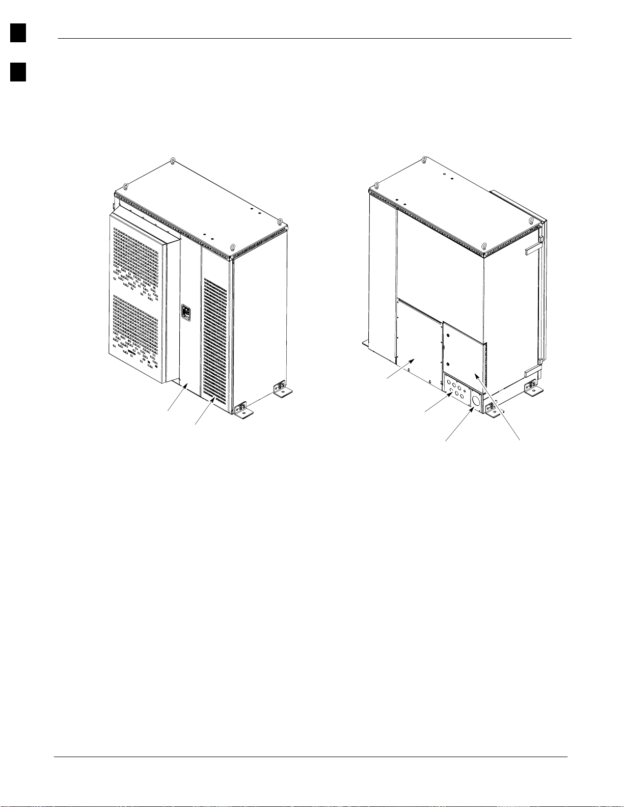
BTS Overview
68P09255A57-2
1
Major Components
The major components that make up the Motorola SC 4812ET are
illustrated in this section: the RF Cabinet (see Figure 1-2) and the Power
Cabinet (see Figure 1-9).
Figure 1-2: SC 4812ET RF Cabinet
Main Door
LPA Door
(Can only be opened after Main Door is open)
RF I/O
Area Cover Plate
Rear Conduit Panel
Rear I/O DoorRear DC Conduit Panel
FW00189
1-16
SC4812ET Optimization/ATP Manual Software Release R16.1.x.x
PRELIMINARY
Aug 2002
Page 43
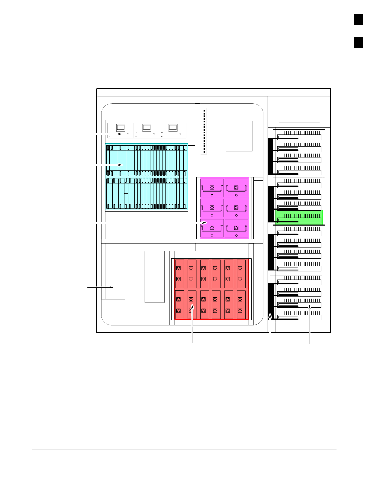
BTS Overview68P09255A57-2
RF Cabinet Internal FRUs
Figure 1-3: RF Cabinet Internal FRUs
CCP Fans
C-CCP Shelf
5 RU Rack Space
Figure 1-3 shows the location of the Internal Field Replaceable
Units (FRUs). A brief description of each Internal FRU is found in the
following paragraphs.
ETIB
RFDS
EBA
1
Combiner
Cage
Circuit
Breaker Panel
DC
Power
Dist.
OPTIONAL AREA
Punch
Block
(back)
DRDC LPAs
LPA Trunking
Backplane
Duplexer/RX Filter Directional Coupler
The DRDC combines, in a single module, the functions of antenna
duplexing, receive band pass filtering, and surge protection (see
Figure 1-7).
FW00163
Aug 2002
Combiner Cage (2:1, 4:1, or Band pass Filter)
The Combiner Cage holds the transmit band pass filters, 2:1 combiners,
or 4:1 combiners, depending on system configuration.
SC4812ET Optimization/ATP Manual Software Release R16.1.x.x
PRELIMINARY
1-17
Page 44

BTS Overview
68P09255A57-2
1
Combined CDMA Channel Processor Shelf
The C-CCP shelf contains the following (see Figure 1-4):
High Stability Oscillator (HSO) or Low Frequency Receiver (LFR)
card (1)
Clock Synchronization Manager (CSM) cards (2)
CDMA Clock Distribution (CCD) cards (2)
Power Supply cards (2 minimum, 3 maximum)
Multicoupler Preselector Cards (MPC) or Expansion Multicoupler
Preselector Cards (EMPC) (2)
Alarm Monitoring and Reporting (AMR) cards (2)
Multi Channel CDMA (MCC8E, MCC24E or MCC-1X) cards (up to
12)
Broadband Transceiver (BBX2 or BBX-1X) cards (up to 13)
Combined Input/Output (CIO) card (1)
Group Line Interface (GLI3) cards (2)
BBX Switch card (1)
Modem (optional)
Filler Panels (as required)
Fan Module (3)
Figure 1-4: SC 4812ET C-CCP Shelf
GLI3GLI3
AMR
AMR
MCC24-1
MCC24-7
Power Supply
19 mm Filter Panel
CSM
HSO/LFR
Power Supply
CSM
CCD CCD
Power Supply
MODEM
MCC24-3
MCC24-2
MCC24-9
MCC24-8
MCC24-5
MCC24-4
MCC24-11
MCC24-10
BBX2-1
MCC24-6
BBX2-7
MCC24-12
BBX2-2
BBX2-3
BBX2-8
BBX2-9
BBX2-4
BBX2-5
BBX2-11
BBX2-10
BBX2-6
BBX2-RSwitch
BBX2-12
CIO
MPC/EMPC-1MPC/EMPC-2
SC 4812ET RF Cabinet
ETIB
5 RU RACK
SPACE
NOTE: MCCs may be
MCC8Es, MCC24Es
or MCC-1Xs. BBXs
may be BBX2s or
BBX-1Xs.
EBA
RFDS
1-18
REF FW00304
Punch Block
The Punch Block is the interface point of the RF Cabinet between the
T1/E1 span lines, the Customer I/O, alarms, multi-cabinet timing
(RGPS and HSO), and Pilot Beacon control (optional). (see Figure 1-6).
SC4812ET Optimization/ATP Manual Software Release R16.1.x.x
PRELIMINARY
Aug 2002
Page 45

BTS Overview68P09255A57-2
Span I/O Board
The Span I/O Board provides the interface for the span lines from the
CSU to the C-CCP backplane (see Figure 1-6).
RF Diagnostic Subsystem
The RFDS provides the capability for remotely monitoring the status of
the SC 4812ET RF Transmit and Receive paths (Figure 1-7).
Heat Exchanger
The Heat Exchanger provides cooling to the internal compartment of the
RF Cabinet. The fan speed of the heat exchangers adjusts automatically
with temperature. The Heat Exchanger is located in the primary front
door of the RF Cabinet.
SC 4812ET Interface Board (ETIB) & LPA Control Brd
(LPAC)
The ETIB is an interconnect board showing status LEDs for the RF
Cabinet, as well as providing secondary surge protection. The LPAC
board provides the interface for the LPA connection.
1
SC 4812ET Trunking Backplane
The Trunking Backplane contains a complex passive RF network that
allows RF signals to share the resources of a bank of four LPAs. It also
provides DC Power and digital interconnect.
Figure 1-5: SC 4812ET Intercabinet I/O Detail (Rear View)
RF CABINET
(Rear View)
Exp. Punch
Block
Punch
RF Expansion
1-3 Sector Antennas
4-6 Sector Antennas
RFDS Expansion
Block
27V
27V Ret
Microwave
RF GPS
LAN
2 Sec Tick
19 MHz Clock
RF CABINET
(Rear Door closed)
FW00147
Aug 2002
Ground Cable
Lugs
Expansion 1
Expansion 2
RFGPS
RGPS
Span/Alarm
DC Conduit
Pilot Beacon
SPAN I / O
SC4812ET Optimization/ATP Manual Software Release R16.1.x.x
PRELIMINARY
1-19
Page 46

BTS Overview
68P09255A57-2
1
Figure 1-6: SC 4812ET I/O Plate Diagram
1A 2A 3A 1B 2B 3B
4A 5A 6A 4B 5B 6B
RF Expansion Ports
1A 2A 3A 1B 2B 3B
Remote
ASU
1
2
4A 5A 6A 4B 5B 6B
Antenna’s
GND
Lugs
50 Pair
Punch
Block
(Alarms/Spans)
Spans
Alams
Modem
20 Pair
Punchblock
RGD/RGPS
Microwave
RF
GPS
LAN
IN OUT
A
B
19 MHz
(RGPS)
2 Sec
RGD
Board
Power Input
+27V
Power Input
27V Ret
FW00171
1-20
SC4812ET Optimization/ATP Manual Software Release R16.1.x.x
PRELIMINARY
Aug 2002
Page 47

BTS Overview68P09255A57-2
Figure 1-7: RFDS Location in an SC 4812ET RF Cabinet
FRONT VIEW
(door not shown for clarity)
RFDS
1
WALL
MOUNTING
BRACKET
DRDC CAGE
DRDC
BTS
CPLD
ANT
CPLD
1B2B3B
4B5B6B
1A2A3A
4A5A6A
Aug 2002
FW00170
SC4812ET Optimization/ATP Manual Software Release R16.1.x.x
PRELIMINARY
1-21
Page 48

Sector Configuration
68P09255A57-2
1
Sector Configuration
Number of
carriers
1 3 or 6 N/A Bandpass Filter, Cavity Combiner (2:1 or 4:1)
2 6 Non-adjacent Cavity Combiner (2:1 Only)
2 6 Adjacent Dual Band Pass Filter
2 3 Non-adjacent Cavity Combiner (2:1 or 4:1)
2 3 Adjacent Bandpass Filter
3,4 3 Non-adjacent Cavity Combiner (2:1 or 4:1)
3,4 3 Adjacent Cavity Combiner (2:1 Only)
Number of
sectors
There are a number of ways to configure the BTS frame. Table 1-5
outlines the basic requirements. When carrier capacity is greater than
two, a 2:1 or 4:1 cavity combiner must be used. For one or two carriers,
bandpass filters or cavity combiners may be used, depending on
sectorization and channel sequencing.
Table 1-5: BTS Sector Configuration
Channel spacing Filter requirements
NOTE
The matrix in Table 1-6 shows a correlation between the various sector
configurations and BBX cards.
In Table 1-6, BBXs may be BBX2s or BBX-1Xs.
1-22
SC4812ET Optimization/ATP Manual Software Release R16.1.x.x
PRELIMINARY
Aug 2002
Page 49

Sector Configuration68P09255A57-2
Table 1-6: Sector Configurations
Config Ref. No. Description
3-Sector/2-ADJACENT Carriers - The configuration below maps TX with optional 2:1 cavity
combiners for 3 sectors/2 carriers for adjacent channels. Note that 2:1 cavity combiners are used (6
total).
1
2
3
4
5
6
7
TX1 TX2 TX3 TX4 TX5 TX6 Carrier#
BBX-1 BBX-2 BBX-3 N/A N/A N/A 1
N/A N/A N/A BBX-4 BBX-5 BBX-6 2
6-Sector/2-NON-ADJACENT Carriers - The configuration below maps TX with 2:1 cavity
combiners for 6 sectors/2 carriers for non-adjacent channels.
TX1 TX2 TX3 TX4 TX5 TX6 Carrier#
BBX-1 BBX-2 BBX-3 BBX-4 BBX-5 BBX-6 1
BBX-7 BBX-8 BBX-9 BBX-10 BBX-11 BBX-12 2
3-Sector/2-NON-ADJACENT Carriers - The configuration below maps TX with 2:1 cavity
combiners for 3 sectors/2 carriers for non-adjacent channels.
TX1 TX2 TX3 TX4 TX5 TX6 Carrier#
BBX-1 BBX-2 BBX-3 N/A N/A N/A 1
BBX-7 BBX-8 BBX-9 N/A N/A N/A 2
3-Sector/4-ADJACENT Carriers - The configuration below maps TX with 2:1 cavity combiners
for 3 sector/4 carriers for adjacent channels.
TX1 TX2 TX3 TX4 TX5 TX6 Carrier#
BBX-1 BBX-2 BBX-3 N/A N/A N/A 1
BBX-7 BBX-8 BBX-9 N/A N/A N/A 2
N/A N/A N/A BBX-4 BBX-5 BBX-6 3
N/A N/A N/A BBX-10 BBX-11 BBX-12 4
3-Sector / 2-ADJACENT Carriers - The configuration below maps TX with bandpass filters for
3 sectors/2 carriers for adjacent channels.
TX1 TX2 TX3 TX4 TX5 TX6 Carrier#
BBX-1 BBX-2 BBX-3 N/A N/A N/A 1
N/A N/A N/A BBX-7 BBX-8 BBX-9 2
3-Sector/3 or 4-NON-ADJACENT Carriers - The configuration below maps TX with 4:1
cavity combiners for 3 sectors/3 or 4 carriers for non-adjacent channels.
TX1 TX2 TX3 TX4 TX5 TX6 Carrier#
BBX-1 BBX-2 BBX-3 N/A N/A N/A 1
BBX-7 BBX-8 BBX-9 N/A N/A N/A 2
BBX-4 BBX-5 BBX-6 N/A N/A N/A 3
BBX-10 BBX-11 BBX-12 N/A N/A N/A 4
6-Sector/1-Carrier - The configuration below maps TX with either bandpass filters or 2:1 cavity
combiners for 6 sector/1 carrier.
TX1 TX2 TX3 TX4 TX5 TX6 Carrier#
BBX-1 BBX-2 BBX-3 BBX-4 BBX-5 BBX-6 1
1
Aug 2002
SC4812ET Optimization/ATP Manual Software Release R16.1.x.x
PRELIMINARY
1-23
Page 50
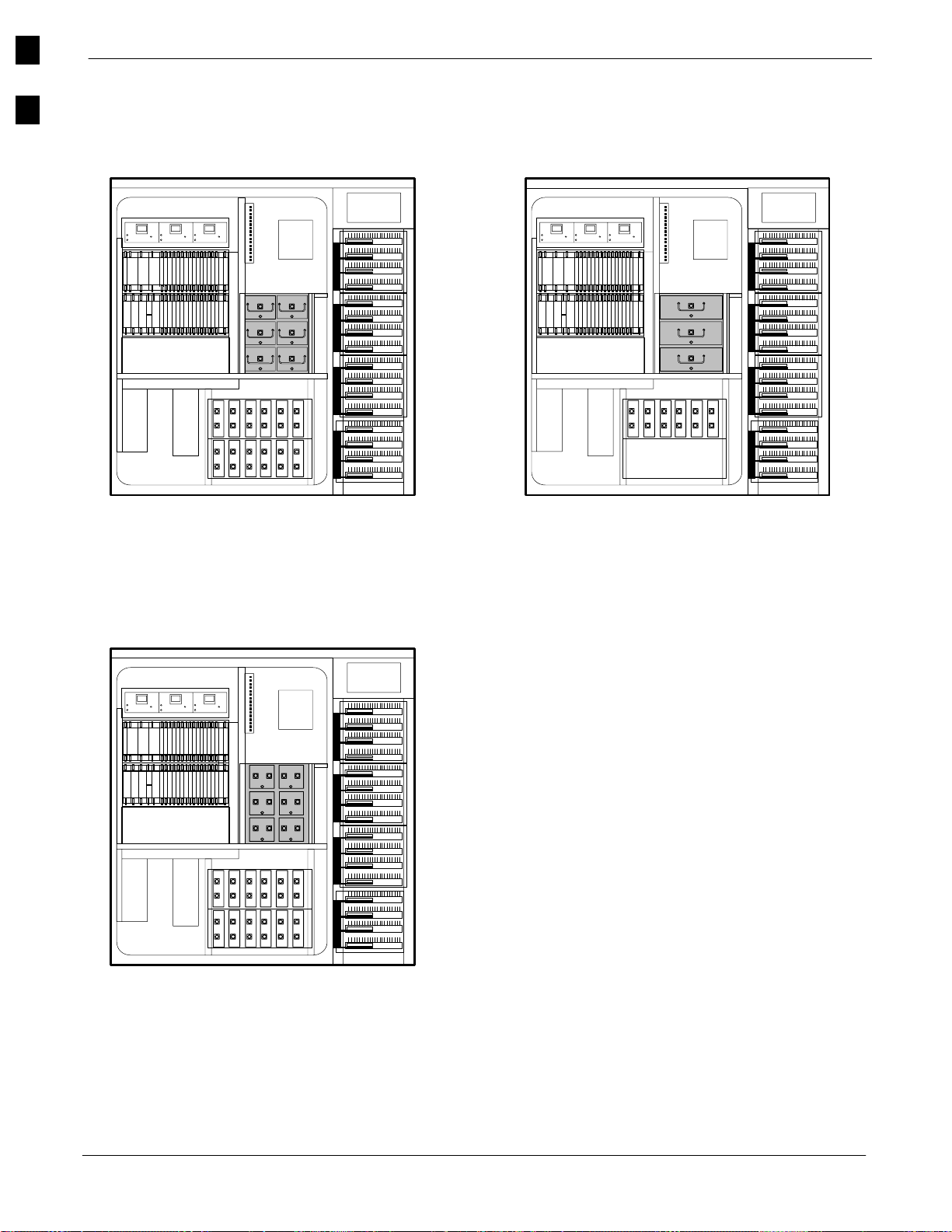
Sector Configuration
68P09255A57-2
1
Figure 1-8: SC4812ET LPA Configuration with Combiners/Filters
EBA
Sector
Numbering
3 Sector
(6 Sector)
C1, S1-S3
(C1, S1-S3)
C2, S1-S3
(C2, S1-S3)
C3, S1-S3
(C1, S4-S6)
C4, S1-S3
(C2, S4-S6)
5 RU RACK
SPACE
2 to 1 Combiner
3 Sector or 6 Sector
ETIB
RFDS
5 RU RACK
SPACE
4 to 1 Combiner
3 Sector Only
ETIB
RFDS
EBA
C1
C2
C3
C4
Dual Bandpass Filter
3 Sector 2 Carrier Maximum
6 Sector 1 Carrier Maximum
5 RU RACK
SPACE
ETIB
RFDS
EBA
Sector
Numbering
3 Sector
(6 Sector)
C1, S1-S3
(C1, S1-S3)
C2, S1-S3
(C2, S1-S3)
C3, S1-S3
(C1, S4-S6)
C4, S1-S3
(C2, S4-S6)
REF. FW00166
1-24
SC4812ET Optimization/ATP Manual Software Release R16.1.x.x
PRELIMINARY
Aug 2002
Page 51
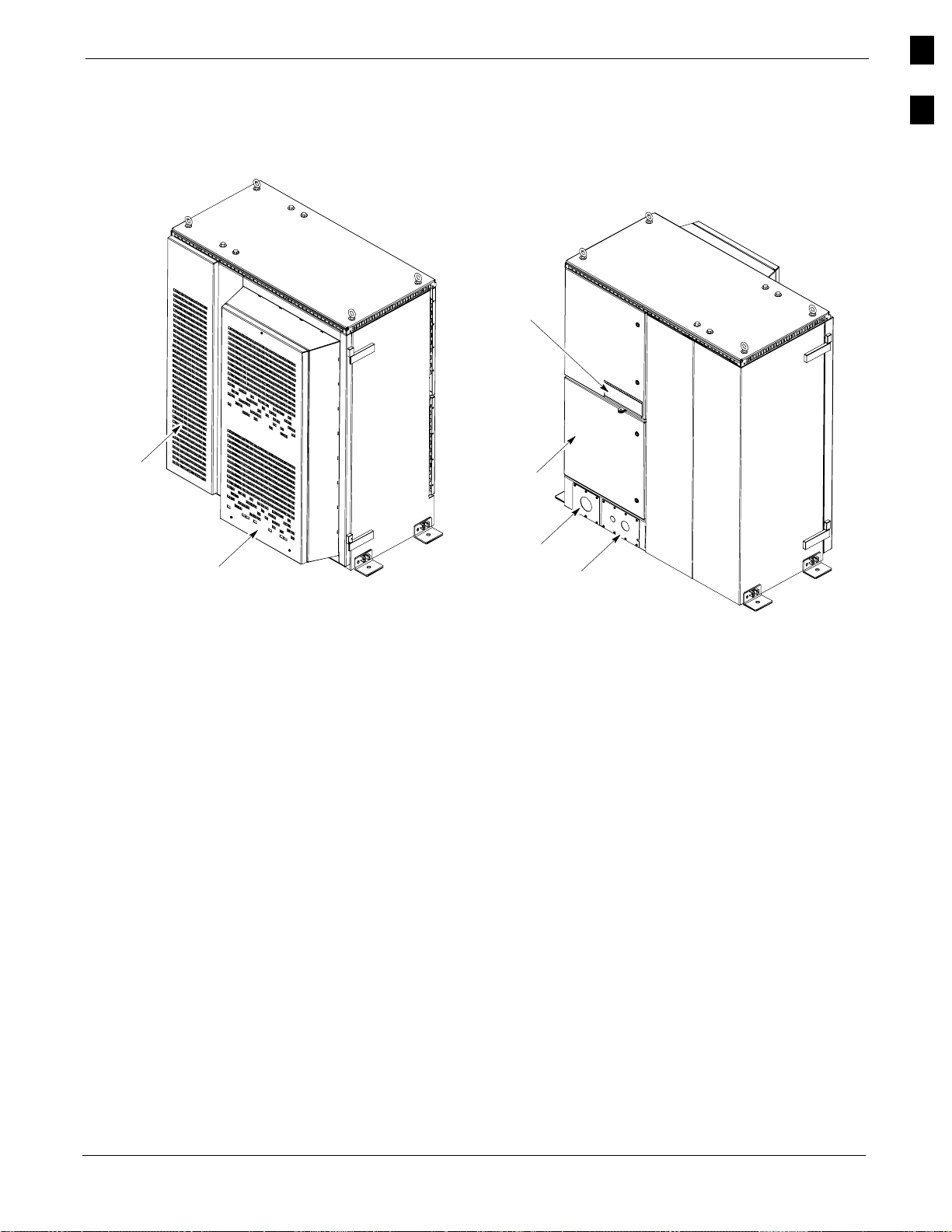
Power Cabinet68P09255A57-2
Power Cabinet
Figure 1-9: Power Cabinet
Battery Door
1
Figure 1-9 illustrates the Power Cabinet design.
GFCI Outlet
Cover
Rear I/O
Door
Main Door
Rear DC
Conduit Panel
Rear AC Conduit
Panel
FW00193
Aug 2002
SC4812ET Optimization/ATP Manual Software Release R16.1.x.x
PRELIMINARY
1-25
Page 52
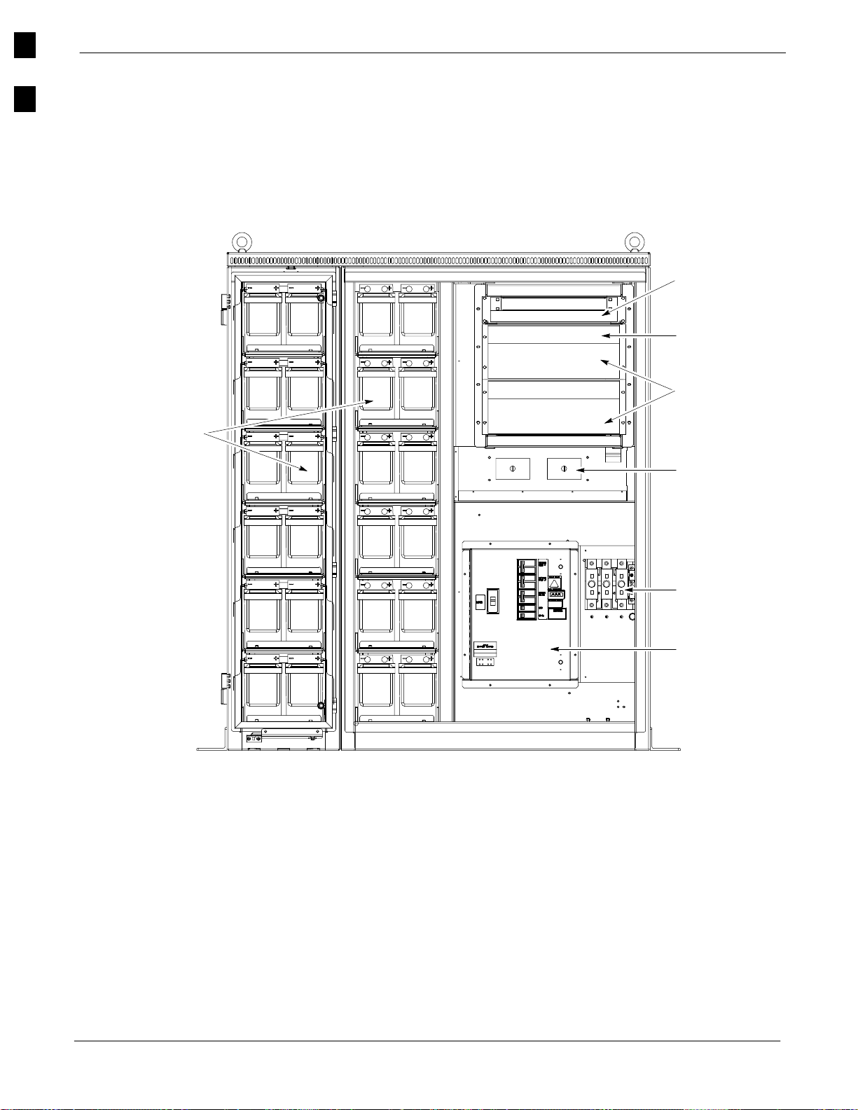
Power Cabinet
68P09255A57-2
1
Internal FRUs
Figure 1-10 shows the location of the Internal Field Replaceable
Units (FRUs). A brief description of each Internal FRU is found in the
following paragraphs.
Figure 1-10: Power Cabinet with Batteries Installed (Doors Removed for Clarity)
Rectifier
Alarm Module
Temperature
Control Module
Rectifier
Shelves
Batteries (Battery
Heaters located
under batteries)
GFCI Outlets
(Back)
NOTE
Punch Block is not
visible in this view.
DC Circuit
Breakers
AC Load
Center
FW00164
FRONT VIEW POWER CABINET
Batteries
The batteries provide a +27 Vdc backup to the RF Cabinet should AC
Power be lost. The Power Cabinet can accommodate a total of 24 12-V
batteries, configured in 12 strings of 2 batteries each. The time duration
of backup provided depends on system configuration.
Battery Heater
1-26
The battery heaters provide heating to the batteries in the Power Cabinet.
A separate heater is required for each string of batteries. The heater is a
pad the batteries sit on located top of each battery shelf. The number of
heaters is dependent on system configuration.
SC4812ET Optimization/ATP Manual Software Release R16.1.x.x
PRELIMINARY
Aug 2002
Page 53

Power Cabinet68P09255A57-2
Battery Compartment Fan
The battery compartment fan provides air circulation for the two battery
compartments. It is located on the inside of the battery compartment
door.
Heat Exchanger
The Heat Exchanger provides cooling to the rectifier compartment of the
Power Cabinet. The Heat Exchanger is located in the primary front door
of the Power Cabinet.
Rectifiers
The +27 Vdc rectifiers convert the AC power supplied to the Power
Cabinet to +27 Vdc to power the RF Cabinet and maintain the charge of
the batteries.
AC Load Center
The ACLC is the point of entry for AC Power to the Power Cabinet. It
incorporates AC power distribution and surge protection.
Punch Block
1
The Punch Block is the interface for the alarm signalling between the
Power Cabinet and the RF Cabinet.
Aug 2002
SC4812ET Optimization/ATP Manual Software Release R16.1.x.x
PRELIMINARY
1-27
Page 54

Power Cabinet
68P09255A57-2
1
Notes
1-28
SC4812ET Optimization/ATP Manual Software Release R16.1.x.x
PRELIMINARY
Aug 2002
Page 55

Chapter 2
Power Up Procedures
2
Aug 2002
SC4812ET Optimization/ATP Manual Software Release R16.1.x.x
PRELIMINARY
2-1
Page 56

Prepower-up
68P09255A57-2
Prepower-up
This section first verifies proper frame equipage. This includes verifying
module placement, jumper, and dual in-line package (DIP) switch
settings against the site-specific documentation supplied for each BTS
2
Cellsite Types
CDF
application. Next, pre-power up and initial power-up procedures are
presented.
Sites are configured as with a maximum of 4 carriers, 3-sectored with a
maximum of 4 carriers, and 6-sectored with a maximum of 2 carriers.
Each type has unique characteristics and must be optimized accordingly.
The Cell-site Data File (CDF) contains site type and equipage data
information and passes it directly to the LMF during optimization. The
number of modem frames, C-CCP shelves, BBX and MCC boards (per
cage), and linear power amplifier assignments are some of the equipage
data included in the CDF.
Site Equipage Verification
Review the site documentation. Match the site engineering equipage data
to the actual boards and modules shipped to the site. Physically inspect
and verify the equipment provided for the BTS or Modem frame and
ancillary equipment frame.
CAUTION
Always wear a conductive, high impedance wrist strap while
handling any circuit card/module to prevent damage by ESD.
After removal, the card/module should be placed on a conductive
surface or back into the anti-static bag it was shipped in.
Initial Installation of Boards/Modules
Table 2-1: Initial Installation of Boards/Modules
Step Action
1 Refer to the site documentation and install all boards and modules into the appropriate shelves as
required. Verify they are NOT SEATED at this time.
2 As the actual site hardware is installed, record the serial number of each module on a “Serial Number
Checklist” in the site logbook.
2-2
SC4812ET Optimization/ATP Manual Software Release R16.1.x.x
PRELIMINARY
Aug 2002
Page 57

Setting Frame C-CCP Shelf Configuration Switch
If the frame is a Starter BTS, the backplane switch settings behind the
fan module should be set to the ON position (see Figure 2-1).
The switch setting must be verified and set before power is applied to the
BTS equipment.
Figure 2-1: Backplane DIP Switch Settings
Prepower-up68P09255A57-2
2
ON
OFF
ON
OFF
RIGHT / LEFT
BOTTOM / TOP
ON
OFF
EXPANSION
FRAME 1
SETTING
SC 4812ET
MODEM_FRAME_ID_1
C-CCP SHELF
MODEM_FRAME_ID_0
EXPANSION
FRAME 2
SETTING
STARTER FRAME
5 RU RACK SPACE
FAN MODULE
REMOVED
ETIB
RFDS
EBA
RIGHT / LEFT
BOTTOM / TOP
MODEM_FRAME_ID_1
MODEM_FRAME_ID_0
Checking for shorts
Aug 2002
SC4812ET Optimization/ATP Manual Software Release R16.1.x.x
FW00167
The following information is used to check for any electrical short
circuits and to verify the operation and tolerances of the cellsite and BTS
power supply units before applying power for the first time. It contains
instructional information on the initial proper power up procedures for
the SC 4812ET power cabinet and RF cabinet. Also presented are tests
to be performed on the power cabinet. Please pay attention to all
cautions and warning statements in order to prevent accidental injury to
personnel.
2-3
PRELIMINARY
Page 58

Prepower-up
68P09255A57-2
Required Tools
The following tools are used in the procedures.
DC current clamp (600 Amp capability with jaw size to accommodate
2/0 cable).
2
Hot Air Gun - (optional for part of the Alarm Verification)
Digital Multimeter (DMM)
Cabling Inspection
Using the site-specific documentation generated by Motorola Systems
Engineering, verify that the following cable systems are properly
connected:
Receive RF cabling - up to 12 RX cables
Transmit RF cabling - up to six TX cables
NOTE
For positive power applications (+27 V):
The positive power cable is red.
The negative power cable is black. (The black power cable is
at ground potential.)
Initial Inspection and Setup
CAUTION
Table 2-2: Initial Inspection and Setup
Step Action
1 Verify that ALL AC and DC breakers are turned OFF in both the Power and RF cabinets. Verify that
the DC power cables between the Power and RF cabinets are connected with the correct polarity
2 The RED cables connect to the uppermost three (3) terminals (marked +) in both cabinets. Confirm
that the split phase 240/120 AC supply is correctly connected to the AC load center input.
CAUTION
Ensure all battery breakers for unused battery positions are open
(pulled out) during any part of the power up process, and remain
in the off position when leaving the site.
Failure to connect the proper AC feed will damage the surge
protection module inside the AC load center.
AC Power Check
The first task in the power up sequence is to apply AC power to the
Power cabinet. Once power is applied a series of AC Voltage
measurements is required.
Table 2-3: AC Voltage Measurements
Step Action
1 Measure the AC voltages connected to the AC load center (access the terminals from the rear of the
cabinet after removing the AC load center rear panel). See Figure 2-2.
2 Measure the AC voltage from terminal L1 to neutral. This voltage should be in the range of nominally
115 to 120 Vac.
. . . continued on next page
2-4
SC4812ET Optimization/ATP Manual Software Release R16.1.x.x
PRELIMINARY
Aug 2002
Page 59
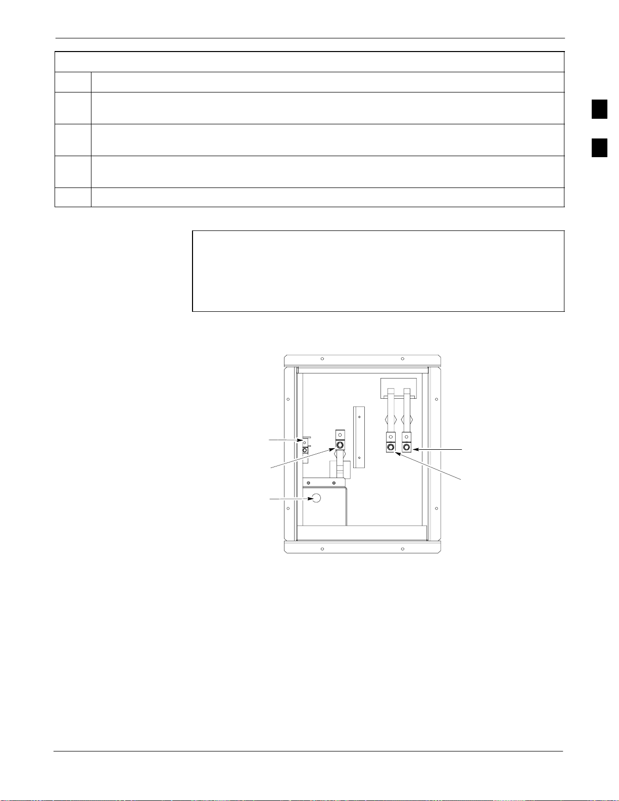
Prepower-up68P09255A57-2
Table 2-3: AC Voltage Measurements
Step Action
3 Measure the AC voltage from terminal L1 to ground. This voltage should be in the range of nominally
115 to 120 Vac.
4 Measure the AC voltage from terminal L2 to neutral. This voltage should be in the range of nominally
115 to 120 Vac.
5 Measure the AC voltage from terminal L2 to ground. This voltage should be in the range of nominally
115 to 120 Vac.
6 Measure L1 - L2 - should be from 208 to 240 Vac.
2
CAUTION
Figure 2-2: AC Load Center Wiring
G = Ground
N = Neutral
L1 = Line 1
L2 = Line 2
AC to Pilot Beacon
If the AC voltages are in excess of 120 V (or exceed 200 V)
when measuring between terminals L1 or L2 to neutral or
ground, STOP and Do Not proceed until the cause of the higher
voltages are determined. The power cabinet WILL be damaged
if the Main breaker is turned on with excessive voltage on the
inputs.
G
N
L1
L2
Aug 2002
FW00305
SC4812ET Optimization/ATP Manual Software Release R16.1.x.x
PRELIMINARY
2-5
Page 60

AC Power Up Sequence
68P09255A57-2
AC Power Up Sequence
Applying AC Power
Once AC Voltage Measurements are complete, apply AC power to the
2
Step Action
1 When the input voltages are verified as correct, turn the Main AC breaker (located on the front of the
ACLC) ON. Observe that all eight (8) green LEDs on the front of the ACLC are illuminated (see
Figure 2-7).
2 Turn Rectifier 1 and Rectifier 2 AC branch breakers (on the AC Load Center) ON. All the installed
rectifier modules (see Figure 2-7) will start up and should each have two green LEDs (DC and Power)
illuminated.
3 Turn the Meter Alarm Panel module, ON (see Figure 2-3), while observing the K2 contact in the
PDA assembly (see Figure 2-9). The contact should close. The Meter Alarm Panel voltage meter
should read approximately 27.4 +
Power Cabinet. Table 2-4 provides the procedure for applying AC
power.
Table 2-4: Applying AC Power
0.2 Vdc.
4 Turn the Temperature Compensation Panel (TCP) ON, (see Figure 2-4). Verify that the Meter Alarm
Control Panel does not have any alarm LEDs illuminated.
5 Check the rectifier current bargraph displays (green LED display on the rectifier module). None
should be illuminated at this point.
NOTE
If batteries are fitted, turn on the two battery heater AC breakers
on the AC Load Center.
Figure 2-3: Meter Alarm Panel
AMP
AMPS
+
-
TEST POINTS
PWR
OFF
ON
FW00245
VOLT
+
-
TEST POINTS
VOLT
FRONT VIEW
Figure 2-4: Temperature Compensation Panel
2-6
TEMPERATURE COMPENSATION PANEL
OFF
ON
1/2 A 250V
ON
SENSOR
COM
12
SENSE
+
-
25 c
FRONT VIEW
SC4812ET Optimization/ATP Manual Software Release R16.1.x.x
PRELIMINARY
V ADJ
FW00246
Aug 2002
Page 61

Power Cabinet Power Tests
Table 2-5: Power Cabinet Power Up Tests
AC Power Up Sequence68P09255A57-2
Table 2-5 lists the step-by-step instructions for Power Up Tests.
Step Action
1 Probe the output voltage test point on the Meter Alarm Panel while pressing the 25° C set button on
the TCP (see Figure 2-4). The voltage should read 27.4 +
Alarm Panel if necessary. Release the TCP 25° C set button.
2 Depending on the ambient temperature, the voltage reading may now change by up to + 1.5 V
compared to the reading just measured. If it is cooler than 25C, the voltage will be higher, and if it is
warmer than 25C, the voltage will be lower.
3 Ensure the RF cabinet 400A main DC breaker is OFF.
4 Close the three (3) Main DC breakers on the Power Cabinet ONLY. Close by holding in the reset
button on the front of the PDA, and engaging one breaker at a time.
5 Measure the voltage between the + and - terminals at the rear of the Power Cabinet and the RF
Cabinet, observing that the polarity is correct. The voltage should be the same as the measurement in
step 2.
6 Place the probes across the black and red battery buss bars in each battery compartment. Place the
probe at the bottom of the buss bars where the cables are connected. The DC voltage should measure
the same as the previous step.
0.2 Vdc. Adjust Master Voltage on Meter
2
Aug 2002
SC4812ET Optimization/ATP Manual Software Release R16.1.x.x
PRELIMINARY
2-7
Page 62

DC Power Pre-test
68P09255A57-2
DC Power Pre-test
DC Power Checks
2
Step Action
1 Physically verify that all AC rectifiers supplying power to the RF cabinets are OFF or disabled (see
Figure 2-5). There should be no 27 Vdc on DC feed terminals.
2 On each RF cabinet:
Unseat all circuit boards/ modules in the distribution shelf, transceiver shelf, and Single Carrier
Linear Power Amplifier (SCLPA) shelves, but leave them in their associated slots.
Unseat all circuit boards (except CCD and CIO cards) in the C-CCP shelf and LPA shelves, but
leave them in their associated slots.
Set C-CCP shelf breakers to the OFF position by pulling out power distribution breakers (labeled
C-CCP 1, 2, 3 - located on the power distribution panel).
Set LPA breakers to the OFF position by pulling out power distribution breakers (8 breakers,
labeled 1A-1B through 4C-4D - located on the power distribution panel).
Before applying any power to the BTS cabinet, verify there are no shorts
in the RF or power DC distribution system (see Figure 2-5).
Table 2-6: DC Power Pre-test (BTS Frame)
3 Verify that the resistance from the power (+) feed terminals with respect to the ground terminal on the
cabinet measures >
500 Ω (see Figure 2-5).
If reading is < 500 Ω, a short may exist somewhere in the DC distribution path supplied by the
breaker. Isolate the problem before proceeding. A reading > 3 M
missing) bleeder resistor (installed across the filter capacitors behind the breaker panel).
Set the 400 Amp Main Breaker and the C-CCP breakers (C-CCP 1, 2, 3) to the ON position by
4
pushing them IN one at a time. Repeat step 3 after turning on each breaker.
Ω could indicate an open (or
* IMPORTANT
If, after inserting any board/module, the ohmmeter stays at 0 Ω, a short probably exists in that
board/module. Replace the suspect board/module and repeat the test. If test still fails, isolate the
problem before proceeding.
Insert and lock the DC/DC converter modules into their associated slots one at a time. Repeat step3
5
after inserting each module.
A typical response is that the ohmmeter will steadily climb in resistance as capacitors charge, finally
indicating approximately 500
Ω.
! CAUTION
Verify the correct power/converter modules by observing the locking/retracting tabs appear as follows:
-
6 Insert and lock all remaining circuit boards and modules into their associated slots in the C-CCP shelf.
Repeat step 3 after inserting and locking each board or module.
2-8
A typical response is that the ohmmeter will steadily climb in resistance as capacitors charge,
stopping at approximately 500
SC4812ET Optimization/ATP Manual Software Release R16.1.x.x
Ω..
. . . continued on next page
PRELIMINARY
Aug 2002
Page 63

DC Power Pre-test68P09255A57-2
Table 2-6: DC Power Pre-test (BTS Frame)
Step Action
7 Set the 8 LPA breakers ON by pushing them IN one at a time. Repeat step 3 after turning on each
breaker.
A typical response is that the ohmmeter will steadily climb in resistance as capacitors charge,
stopping at approximately 500
8 Seat all LPA and associated LPA fan modules into their associated slots in the shelves one at a time.
Repeat step 3 after seating each LPA and associated LPA fan module.
Ω..
A typical response is that the ohmmeter will steadily climb in resistance as capacitors charge,
stopping at approximately 500
9 Seat the Heat Exchanger, ETIB, and Options breakers one at a time. Repeat step 3.
Ω..
RF Cabinet Power Up
Table 2-7 covers the procedures for properly powering up the RF
Cabinet.
2
Table 2-7: RF Cabinet Power Up
Step Action
1 Ensure the 400 Amp Main DC breaker and all other breakers in the RF Cabinet are OFF.
2 Proceed to the DC Power Pre-test (BTS Frame) sequence (see Table 2-6) (for initial power-up as
required).
3 Ensure the power cabinet is turned on (see Table 2-5). Verify that 27 volts is applied to the terminals
on the back of the RF cabinet.
4 Engage the main DC circuit breaker on the RF cabinet (see Figure 2-5).
5 On each RF cabinet:
Set C-CCP shelf breakers to the ON position by pushing them in one at a time (labeled
C-CCP 1, 2, 3 - located on the power distribution panel).
Set LPA breakers to the ON position by pushing them in one at a time (8 breakers, labeled 1A-1B
through 4C-4D - located on the power distribution panel).
Set the two heat exchanger breakers to the ON position by pushing them in one at a time.
Set the ETIB breaker to the ON position by pushing it in.
Set the OPTION breaker to the ON position by pushing it in.
6 Measure the voltage drop between the Power Cabinet meter test point and the 27 V buss bar inside the
RF Cabinet PDA while the RF Cabinet is transmitting.
NOTE
For a 3-sector carrier system, the voltage drop should be less than 0.2 V.
For a 12-sector carrier system, the voltage drop should be less than 0.3 V.
7 Using a DC current probe, measure the current in each of the six (6) DC cables that are connected
between the RF and Power Cabinet. The DC current measured should be approximately the same. If
there is a wide variation between one cable and the others (>20 A), check the tightness of the
connections (torque settings) at each end of the cable.
Aug 2002
SC4812ET Optimization/ATP Manual Software Release R16.1.x.x
PRELIMINARY
2-9
Page 64
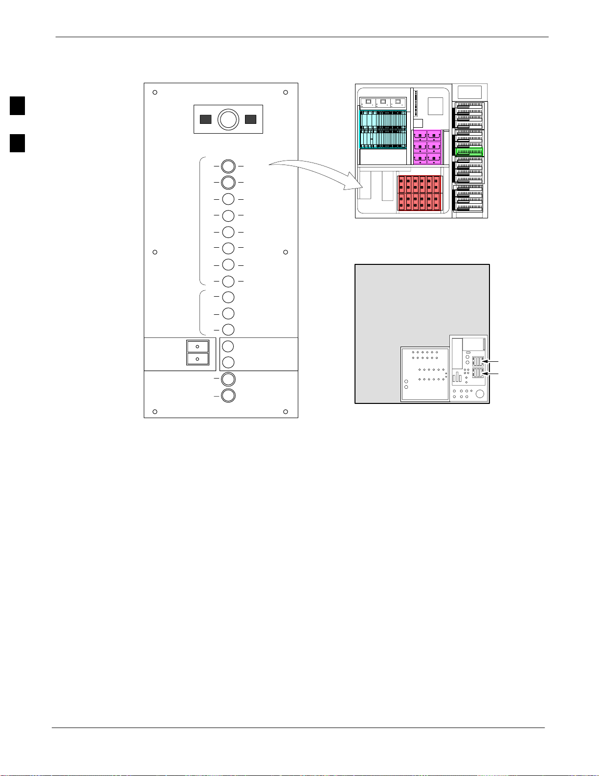
DC Power Pre-test
Figure 2-5: RF Cabinet Circuit Breaker Panel and 27Vdc Terminal Locations
68P09255A57-2
1A
1C
2A
2C
3A
3C
4A
4C
PS1
PS2
PS3
ETIB
400
30
1B
30
1D
30
2B
2D
30
3B
30
30
3D
4B
30
4D
30
50
50
50
HEAT EXCHANGER
25
CAUTION
SHUT OFF BOTH BREAKERS
ONLY DURING HEAT EXCHANGER
25
MAINTENANCE OR REPAIR
10
15
5 RU RACK
SPACE
SC 4812ET BTS RF Cabinet
(Front View)
RF CABINET
(Rear View)
27V
27V Ret
2
MAIN BREAKER
L
P
A
C
C
C
P
LPA
BLOWERS
PUSH BUTTON
TO RESET
LPA BLOWERS
OPTION
FW00307
I/O Plate + and - DC Feed
Terminals (Back Panel of RF
Cabinet)
2-10
SC4812ET Optimization/ATP Manual Software Release R16.1.x.x
PRELIMINARY
Aug 2002
Page 65

Battery Test68P09255A57-2
Battery Test
Charge Test (Connected Batteries)
Table 2-8 lists the step-by-step instructions for testing the batteries.
Table 2-8: Battery Charge Test (Connected Batteries)
Step Action
1 Close the battery compartment breakers for connected batteries ONLY. This process should be
completed quickly to avoid individual battery strings with excess charge current
NOTE
If the batteries are sufficiently discharged, the battery circuit breakers may not engage individually
due to the surge current. If this condition is observed, turn off the Meter Alarm Panel power switch,
and then engage all the connected battery circuit breakers, the Meter Alarm Panel power switch
should then be turned ON.
2 Using the DC current probe, measure the current in each of the battery string connections to the buss
bars in each battery cabinet. The charge current may initially be high but should quickly reduce in a
few minutes if the batteries have a typical new battery charge level.
2
3 The current in each string should be approximately equal (+ 5 A).
4 The bargraph meters on the rectifier modules can be used as a rough estimate of the total battery
charge current. Each rectifier module has eight LEDs to represent the output current. Each illuminated
LED indicates that approximately 12.5% (1/8 or 8.75 A) of the rectifier’s maximum (70 A) current is
flowing.
EXAMPLE:
Question: A system fitted with three rectifier modules each have three bargraph LEDs illuminated.
What is the total output current into the batteries?
Answer: Each bargraph is approximately indicating 12.5% of 70 A, therefore, 3 X 8.75A equals
26.25A. As there are three rectifiers, the total charge current is equal to (3 X 26.25 A) 78.75 A.
This charge current calculation only applies at this part of the start up procedure when the RF Cabinet
is not powered on, and the power cabinet heat exchanger is turned off.
5 Allow a few minutes to ensure that the battery charge current stabilizes before taking any further
action. Recheck the battery current in each string. If the batteries had a reasonable charge, the current
in each string should reduce to less than 5 A.
6 Recheck the DC output voltage. It should remain the same as measured in step 4 of the Power Up
Test.
NOTE
If discharged batteries are installed, all bargraphs may be illuminated on the rectifiers during the
charge test. This indicates that the rectifiers are at full capacity and are rapidly charging the batteries.
It is recommended in this case that the batteries are allowed to charge and stabilize as in the above
step before commissioning the site. This could take several hours.
Aug 2002
SC4812ET Optimization/ATP Manual Software Release R16.1.x.x
PRELIMINARY
2-11
Page 66

Battery Test
Discharge Test
68P09255A57-2
Perform the test procedure in Table 2-9 only when the battery current is
less than 5 A per string. Refer to Table 2-8 for the procedures to check
current levels.
2
Table 2-9: Battery Discharge Test
Step Action
1 Turn the battery test switch on the Meter Alarm Panel, ON (see Figure 2-3). The rectifier output
voltage and current should decrease by approximately 10% as the batteries assume the load. Alarms
for the Meter Alarm Panel may occur.
2 Measure the individual battery string current using the DC current probe. The battery discharge
current in each string should be approximately the same (within± 5 A).
3 Turn Battery Test Switch OFF.
CAUTION
Failure to turn OFF the Battery Test Switch before leaving the
site, will result in low battery capacity and reduce battery life.
2-12
SC4812ET Optimization/ATP Manual Software Release R16.1.x.x
PRELIMINARY
Aug 2002
Page 67
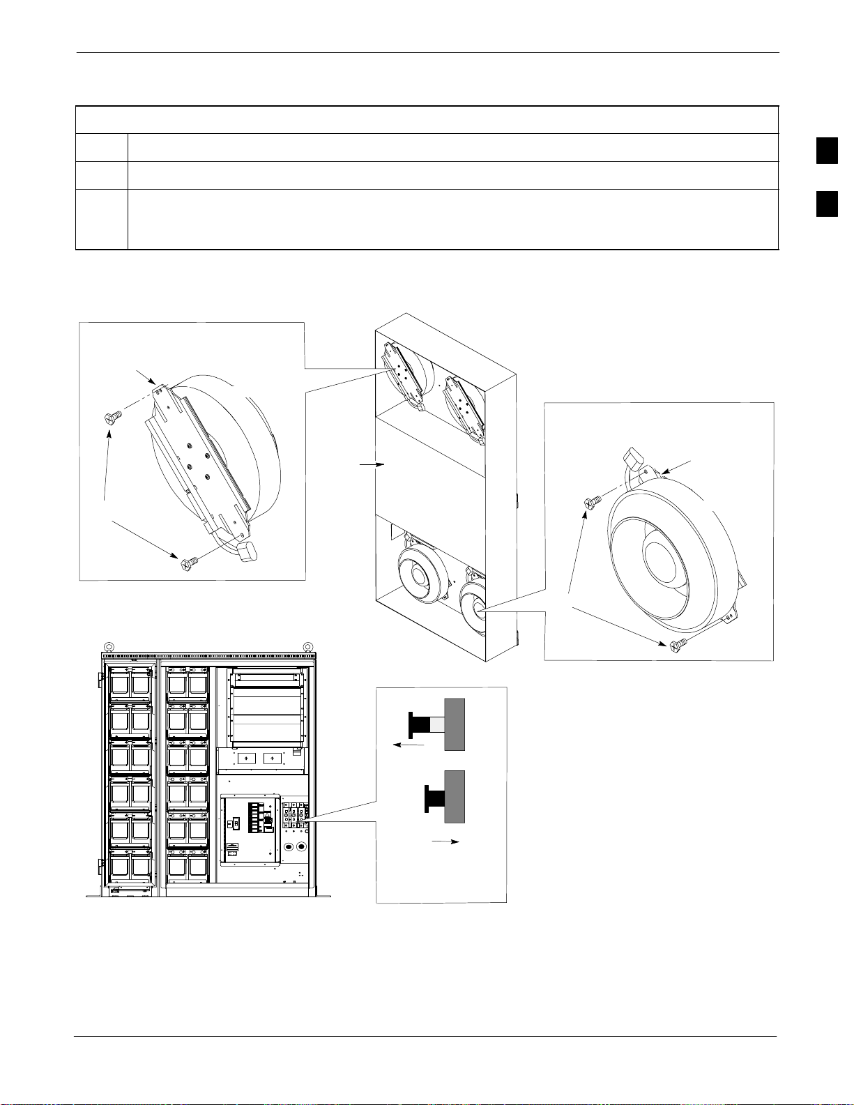
Heat Exchanger Power Up
Table 2-10: Heat Exchanger Power Up
Step Action
Heat Exchanger Power Up68P09255A57-2
1 Turn the Power Cabinet Heat Exchanger breakers ON (seeFigure 2-6 for breaker location).
2 The Heat Exchanger will now go into a five (5) minute test sequence. Ensure that the internal and
external fans are operating. Place a hand on the internal and external Heat Exchanger grills to feel for
air draft.
Figure 2-6: Heat Exchanger Blower Assembly
Heat Exchanger
Bottom (Ambient) Blower
Mounting
Bracket
Fan Module
Core
T-30 Screw
Blower
Power
Cord
Assembly
Top (Internal) Blower
Blower
Power
Cord
2
Mounting
Bracket
Fan Module
POWER CABINET
Front View
OUT=OFF
IN=ON
Blower Assembly
Circuit Breaker
Side View
T-30 Screw
FW00181
Aug 2002
SC4812ET Optimization/ATP Manual Software Release R16.1.x.x
PRELIMINARY
2-13
Page 68
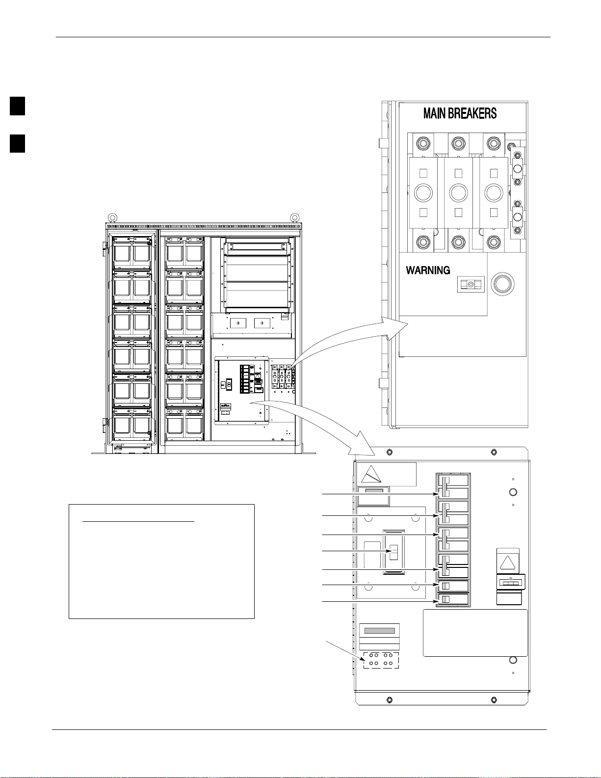
Heat Exchanger Power Up
Figure 2-7: Power Cabinet Circuit Breaker Assemblies
68P09255A57-2
2
DC Circuit
Breaker
A B C
160 160 160
BREAKER SYSTEM BREAKER
SHOULD BE RESET
IF ILLUMINATED OR
AFTER RESET OF
3 MAIN BREAKERS
TO RESET MAIN BREAKERS, PRESS
AND HOLD IN GREEN BUTTON WHILE
PRESSING 160 AMP BREAKER BUTTON
UNTIL LATCHED RELEASE GREEN BUTTON
AFTER ALL 3 BREAKERS HAVE BEEN RESET
ON OFF
BREAKER SYSTEM
BREAKER
SYSTEM RESET
BUTTON
25
25
Circuit Breaker Legend:
1. Main 150 Amp. . . . . . . . . . . . . . .
2. Rectifier Shelf #1 70 Amp. . . .
3. Rectifier Shelf #2 70 Amp. . . .
4. Battery Heater #1 15 Amp. . . .
5. Battery Heater #2 15 Amp. . . .
6. GFCI 15 Amp. . . . . . . . . . . . . . .
7. Spare 15 Amp. . . . . . . . . . . . . .
2-14
POWER CABINET
Front View
ATTENTION
2
3
4
1
MAIN
5
6
7
LED Status
AC Circuit
Breaker
FW00144
SC4812ET Optimization/ATP Manual Software Release R16.1.x.x
PRELIMINARY
RECTIFIER
SHELF #1
RECTIFIER
SHELF #2
BATTERY
HEATER #1
BATTERY
HEATER #2
GFCI
SPARE
CAUTION
LIVE TERMINALS
Aug 2002
Page 69
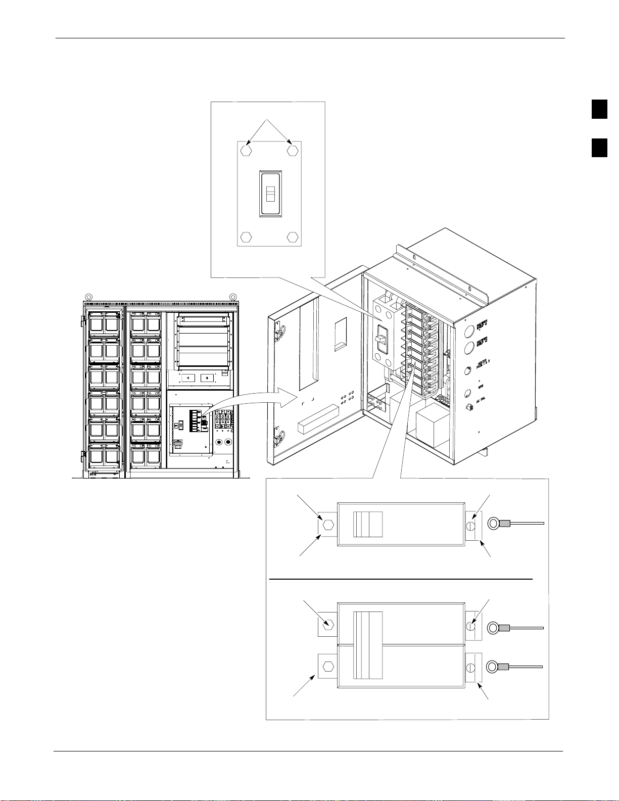
Figure 2-8: Power Cabinet AC Circuit Breakers
7/16 NUT
150 Amp Breaker
Heat Exchanger Power Up68P09255A57-2
2
AC Circuit Breaker
Aug 2002
POWER CABINET
Front View
SC4812ET Optimization/ATP Manual Software Release R16.1.x.x
5/16 NUT
LEFT TAB
5/16 NUT
LEFT TABS
PRELIMINARY
15 Amp Breaker
30 Thru 140 Amp Breaker
SCREW
WIRE
RIGHT TAB
SCREW
WIRE
WIRE
RIGHT
TABS
FW00145
2-15
Page 70
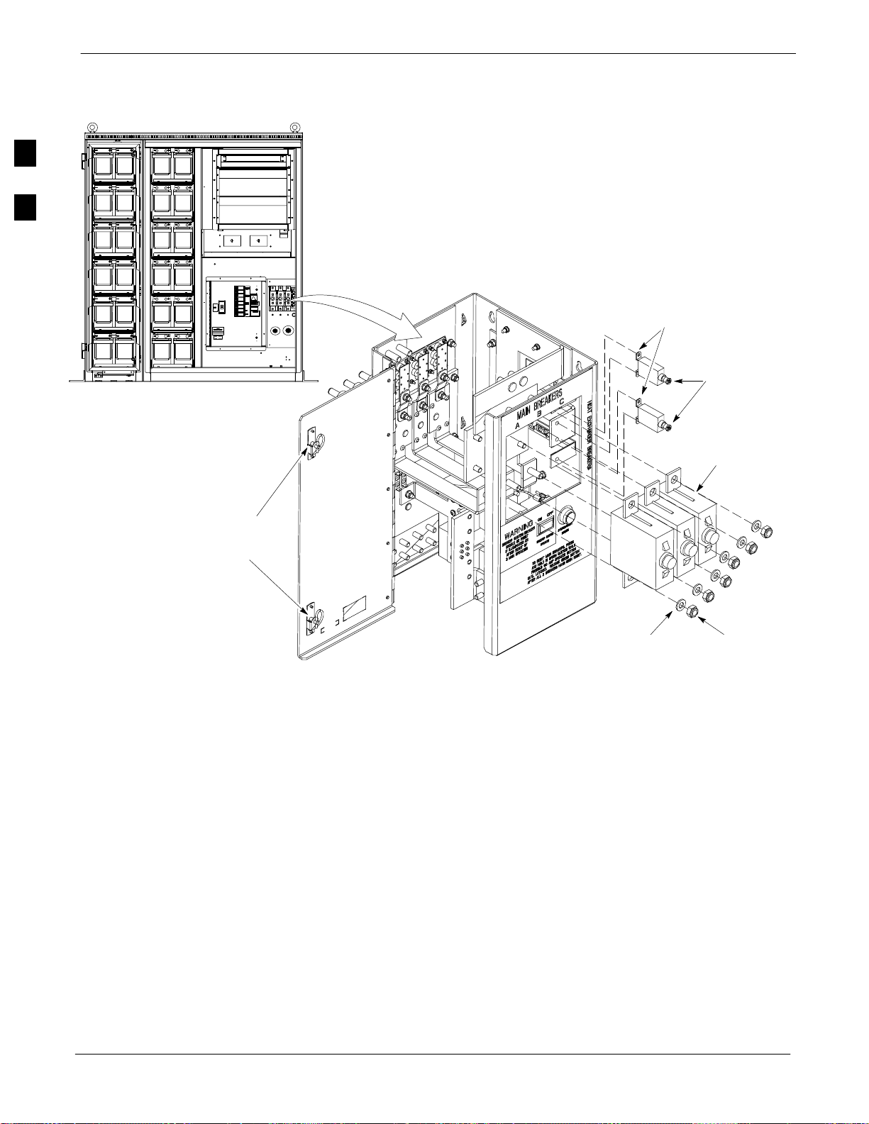
Heat Exchanger Power Up
68P09255A57-2
Figure 2-9: Power Cabinet DC Circuit Breakers
2
DC Circuit Breaker
9/32 Nut
15 AMP
POWER CABINET
Front View
DC Power
Panel Door
Locks
FW00146
Flat Washer
Lock Washer
3x150 AMP
17 mm Nut
2-16
SC4812ET Optimization/ATP Manual Software Release R16.1.x.x
PRELIMINARY
Aug 2002
Page 71

Chapter 3
Optimization/ATP
3
Aug 2002
SC4812ET Optimization/ATP Manual Software Release R16.1.x.x
PRELIMINARY
3-1
Page 72

Basic Optimization
Basic Optimization
Introduction
68P09255A57-2
This chapter provides procedures for downloading system operating
software, set up of the supported test equipment, CSM reference
verification/optimization, and transmit/receive path verification.
NOTE
Before using the LMF, use an editor to view the ”CAVEATS”
section in the ”readme.txt” file in the c:\wlmf folder for any
applicable information.
3
Optimization Process
After a BTS is physically installed and the preliminary operations
(power up) have been completed, the CDMA LMF is used to calibrate
and optimize the BTS. The basic optimization process can be
accomplished as follows:
Download MGLI with code and data and then enable MGLI.
NOTE
Use the status function and verify that all of the installed devices of
Download code and data to all devices of the following types:
Download the RFDS TSIC (if installed).
Verify the operation of the GPS and HSO or LFR signals.
Enable the following devices (in the order listed):
Connect the required test equipment for a full optimization.
Select the test equipment.
Calibrate the TX and RX test cables if they have not previously been
Select all of the BBXs and all of the MCCs and use the full
The GLIs may be GLI2s or GLI3s
the following types respond with status information: CSM, BBX,
GLI3, and MCC (and TSU if RFDS is installed). If a device is
installed and powered up but is not responding and is colored gray in
the BTS display, the device is not listed in the CDF file. The CDF file
will have to be corrected before the device can be accessed by CDMA
LMF.
- CSM
- BBX (may be BBX2 or BBX-1X)
- GLI3 (other than GLI3-1)
- MCC (may be MCC-8E, MCC24, or MCC-1X)
- Secondary CSM (slot 2)
- Primary CSM (slot 1)
- All MCCs
calibrated using the CDMA LMF that is going to be used for the
optimization/calibration. The cable calibration values can also be
entered manually.
optimization function. The full optimization function performs TX
calibration, BLO download, TX audit, all TX tests, and all RX tests
for all selected devices.
3-2
SC4812ET Optimization/ATP Manual Software Release R16.1.x.x
PRELIMINARY
Aug 2002
Page 73

Cell-site Types
Basic Optimization68P09255A57-2
If the TX calibration fails, repeat the full optimization for any failed
paths.
If the TX calibration fails again, correct the problem that caused the
failure and repeat the full optimization for the failed path.
If the TX calibration and audit portion of the full optimization passes
for a path but some of the TX or RX tests fail, correct the problem that
caused the failure and run the individual tests as required until all TX
and RX tests have passed for all paths.
Cell-site Data File
NOTE
Sites are configured as Omni/Omni or Sector/Sector (TX/RX). Each type
has unique characteristics and must be optimized accordingly.
For more information on the different in site types, please refer
to the applicable BTS/Modem Frame Hardware Installation and
Functional Hardware Description manuals.
The Cell-Site Data File (CDF) contains information that defines the
BTS and data used to download files to the devices. A CDF file must be
placed in the applicable BTS folder before the LMF can be used to log
into that BTS. CDF files are normally obtained from the CBSC using a
floppy disk. A file transfer protocol (ftp) method can be used if the LMF
computer has the cabability.
The CDF includes the following information:
Download instructions and protocol
Site specific equipage information
C-CCP shelf allocation plan
- BBX equipage (based on cell-site type) including redundancy
- CSM equipage including redundancy
- MCC (MCC24E, MCC8E or MCC-1X) channel element allocation
plan. This plan indicates how the C-CCP shelf is configured, and
how the paging, synchronization, traffic, and access channel
elements (and associated gain values) are assigned among the (up to
12) MCCs in the shelf.
CSM equipage including redundancy
Effective Rated Power (ERP) table for all TX channels to antennas
respectively. Motorola System Engineering specifies the ERP of a
transmit antenna based on site geography, antenna placement, and
government regulations. Working from this ERP requirement, the
antenna gain, (dependent on the units of measurement specified) and
antenna feed line loss can be combined to determine the required
power at the top of the BTS frame. The corresponding BBX output
level required to achieve that power level on any channel/sector can
also be determined.
3
Aug 2002
NOTE
SC4812ET Optimization/ATP Manual Software Release R16.1.x.x
Refer to the CDMA LMF Operator’s Guide for additional
information on the layout of the LMF directory structure
(including CDF file locations and formats).
PRELIMINARY
3-3
Page 74

Basic Optimization
BTS System Software Download
BTS system software must be successfully downloaded to the BTS
processor boards before optimization can be performed. BTS operating
code is loaded from the LMF computer terminal.
Circuit Backhaul BTS
The information below is for Circuit-Backhaul BTS. GLI-3’s
configured for Circuit-backhaul use bts.cdf files.
68P09255A57-2
NOTE
3
CAUTION
Before using the LMF for optimization/ATP, the correct
bts-#.cdf and cbsc-#.cdf files for the BTS must be obtained
from the CBSC and put in a bts-# folder in the LMF. Failure to
use the correct CDF files can cause wrong results.
Failure to use the correct CDF files to log into a live (traffic
carrying) site can shut down the site.
Packet-Backhaul BTS
GLI-3’s are configured for Packet-backhaul BTS’s the file that is needed
to login to the BTS is the NECF file (bts-xxx.xml) located on the
OMC/R.
The CDF is normally obtained from the CBSC on a DOS formatted
diskette, or through a file transfer protocol (ftp) if the LMF computer has
ftp capability. Refer to the CDMA LMF Operator’s Guide, or the LMF
Help screen, for more information.
Site Equipage Verification
If you have not already done so, use an editor to view the CDF, and
review the site documentation. Verify the site engineering equipage data
in the CDF to the actual site hardware.
CAUTION
Isolate BTS from T1/E1 Spans
NOTE
Each frame is equipped with one 50-pair punch block for spans,
customer alarms, remote GPS, and power cabinet alarms. See Figure 3-2
and refer to Table 3-1 for the physical location and pin call-out
information. To disable the span, pull the surge protectors for the
respective span.
Before connecting the LMF to the frame LAN, the OMC/CBSC must
disable the BTS and place it OOS to allow the LMF to control the
CDMA BTS. This prevents the CBSC from inadvertently sending
control information to the CDMA BTS during LMF based tests.
3-4
SC4812ET Optimization/ATP Manual Software Release R16.1.x.x
Always wear a conductive, high impedance wrist strap while
handling any circuit card/module to prevent damage by ESD.
Extreme care should be taken during the removal and installation
of any card/module. After removal, the card/module should be
placed on a conductive surface or back into the anti-static bag in
which it was shipped.
At active sites, the OMC/CBSC must disable the BTS and place
it out of service (OOS). DO NOT remove the span surge
protectors until the OMC/CBSC has disabled the BTS.
Aug 2002
PRELIMINARY
Page 75

Configure Channel Service Unit
The M-PATH 537 Channel Service Unit (CSU) provides in-band
SNMP-managed digital service access to T1 and fractional T1 lines.
M-PATH units plug into the Kentrox 2-slot frame (see Figure 3-1).
Remote M-PATH management is available via SNMP over an in-band
data link on the T1 line (using a facility data link or 8-64 kbps of a DS0
channel). The unit at the near end of the management path can be an
SNMP manager or another M-PATH CSU.
Each 19 inch rack can support two CSU M-PATH 537 modules. Each
M-PATH 537 module supports one and only one span connection.
Programming of the M-PATH is accomplished through the DCE 9-pin
connector on the front panel of the CSU shelf. Manuals and a Microsoft
Windows programming disk is supplied with each unit.
Setting the Control Port
Whichever control port is chosen, it must first be set up so the control
port switches match the communication parameters being used by the
control device. If using the rear-panel DTE control port, set the
shelf-address switch SA5 to “up” (leave the switch down for the
rear-panel DCE control port).
Configure Channel Service Unit68P09255A57-2
3
For more information, refer to the vendor user manual (part number
1174139) and installation manual (part number 1174462) provided with
each CSU.
Plug one of the cables listed below into the Control Port connectors:
Part Number Description of Cable
01-95006-022 (six feet) DB-9S to DB-9P
01-95010-022 (ten feet)
The control port cables can be used to connect the shelf to:
A PC using the AT 9-pin interface
A modem using the 9-pin connector
Other shelves in a daisy chain
Aug 2002
SC4812ET Optimization/ATP Manual Software Release R16.1.x.x
PRELIMINARY
3-5
Page 76

Configure Channel Service Unit
Figure 3-1: Back and Front View of the CSU
68P09255A57-2
To/From
Network
T1 DDS T1 DDS
NETWORK NETWORK
3
To/From
GLI
DTE DCEDATA PORT DATA PORT
T1 TERMINAL T1 TERMINAL
CONTROL
PORT
To/From
Network
GROUP
ADDRESS
SLOT 1SLOT 2
To/From
GLI
SHELF
ADDRESS
Back View
SLOT 1 SLOT 2
DCE Connector
(Craft Port)
CAUTION
Front View
SC4812ET Span Line Labeling for Span B and Span C is
REF. FW00212
swapped
-On the SC4812ET’s, the span cable internal to the base station
that connects the 50 pin header on the I/O plate to the CSU has
Span B and Span C (RJ-45) connectors mis-labeled.
-CFE will punch down the span on the 50 pair bunchblock as per
Motorola documentation and punchdown chart. When conecting
the span input to the CSU re-label “Span B” cable to”Span C”
cable to “Span B”. Connect to CSU as per documentation
Note: The labeling issue on the cable from the I/O plate to the
CSU Part Number 3086601H01 Rev C shall be corrected on
revision “D” to address this issue. The cut over date to Rev. D
will be approximately January 30, 2001.
3-6
SC4812ET Optimization/ATP Manual Software Release R16.1.x.x
PRELIMINARY
Aug 2002
Page 77

Alarm and Span Line Cable Pin/Signal Information68P09255A57-2
Alarm and Span Line Cable Pin/Signal Information
See Figure 3-2 and refer toTable 3-1for the physical location and pin
call-out information for the 50-pin punch block.
Figure 3-2: 50 Pair Punch Block
STRAIN RELIEVE INCOMING
CABLE TO BRACKET WITH
TIE WRAPS
TO MODEM
CONNECTOR
TO LAN
CONNECTOR
TO ALARMS
CONNECTOR
3
RF Cabinet I/O Area
TO RGD/RGPS
CONNECTOR
1T = PAIR 1 - TIP
1R = PAIR 1 -RING
” ”
” ”
” ”
12
1T 1R 2T 2R
LEGEND
2R
2T
1R
1T
49T
49R
50T
50R
Aug 2002
TOP VIEW OF PUNCH BLOCK
SC4812ET Optimization/ATP Manual Software Release R16.1.x.x
PRELIMINARY
FW00162
3-7
Page 78

Alarm and Span Line Cable Pin/Signal Information
Alarm and Span Line Cable Pin/Signal Information
Table 3-1 lists the complete pin/signal identification for the 50-pin
punch block.
Table 3-1: Pin-Out for 50-Pair Punchblock
68P09255A57-2
Punchblock
Cable
Function
Signal Name Punch Pin Ext. Cable Wire
Color
Connector
Power Cab Control - NC 1T Blue
3
Power Cab Control - NO 1R Blk/Blue
Power Cab Control-Com 2T Yellow
Reserved 2R N/C
Rectifier Fail 3T Blk/Yellow
AC Fail 3R Green
Power Cabinet
ALARM
HSO/LFR
Extension
Power Cab Exchanger Fail 4T Blk/Grn
Power Cab Door Alarm 4R White
Power Cab Major Alarm 5T Blk/White
Battery Over Temp 5R Red
Power Cab Minor Alarm 6T Blk/Red
Reticifier Over Temp 6R Brown
Power Cab Alarm Rtn 7T Blk/Brn
LFR_HSO_GND 7R
EXT_1PPS_POS 8T
EXT_1PPS_NEG 8R
LFR Antenna
Pilot Beacon
CAL_+ 9T
CAB_- 9R
LORAN_+ 10T
LORAN_- 10R
Pilot Beacon Alarm - Minor 11T
Pilot Beacon Alarm - Rtn 11R
Pilot Beacon Alarm - Major 12T
Pilot Beacon Control-NO 12R
Pilot Beacon Control - COM 13T
Pilot Beacon Control - NC 13R
. . . continued on next page
3-8
SC4812ET Optimization/ATP Manual Software Release R16.1.x.x
PRELIMINARY
Aug 2002
Page 79

Alarm and Span Line Cable Pin/Signal Information68P09255A57-2
Table 3-1: Pin-Out for 50-Pair Punchblock
Punchblock
Cable
Function
Connector
ALARM Customer Outputs
Punch PinSignal Name
Customer Outputs 1 - NO 14T
Customer Outputs 1 - COM 14R
Customer Outputs 1 - NO 14T
Customer Outputs 1 - COM 14R
Customer Outputs 1 - NC 15T
Customer Outputs 2 - NO 15R
Customer Outputs 2 - COM 16T
Customer Outputs 2 - NC 16R
Customer Outputs 3 - NO 17T
Customer Outputs 3 - COM 17R
Customer Outputs 3 - NC 18T
Customer Outputs 4 - NO 18R
Customer Outputs 4-COM 19T
Customer Outputs 4 - NC 19R
Customer Inputs 1 20T
Ext. Cable Wire
Color
3
ALARM Customer Inputs
Cust_Rtn_A_1 20R
Customer Inputs 2 21T
Cust_Rtn_A_2 21R
Customer Inputs 3 22T
Cust_Rtn_A_3 22R
Customer Inputs 4 23T
Cust_Rtn_A_4 23R
Customer Inputs 5 24T
Cust_Rtn_A_5 24R
Customer Inputs 6 25T
Cust_Rtn_A_6 25R
Customer Inputs 7 26T
Cust_Rtn_A_7 26R
Customer Inputs 8 27T
Cust_Rtn_A_8 27R
Customer Inputs 9 28T
Cust_Rtn_A_9 28R
Aug 2002
Customer Inputs 10 29T
Cust_Rtn_A_10 29R
. . . continued on next page
SC4812ET Optimization/ATP Manual Software Release R16.1.x.x
PRELIMINARY
3-9
Page 80

Alarm and Span Line Cable Pin/Signal Information
Table 3-1: Pin-Out for 50-Pair Punchblock
68P09255A57-2
Punchblock
Cable
Punch PinSignal Name
Function
Ext. Cable Wire
Color
Connector
RCV_TIP_A 30T
RCV_RING_A 30R
Span 1
XMIT_TIP_A 31T
XMIT_RING_A 31R
RCV_TIP_B 32T
3
Span 2
RCV_RING_B 32R
XMIT_TIP_B 33T
XMIT_RING_B 33R
RCV_TIP_C (Note) 34T
RCV_RING_C (Note) 34R
Span 3
XMIT_TIP_C (Note) 35T
XMIT_RING_C(Note) 35R
RCV_TIP_D (Note) 36T
SPAN I/O
RCV_RING_D (Note) 36R
Span 4
XMIT_TIP_D (Note) 37T
Span 5
Span 6
XMIT_RING_D(Note) 37R
RCV_TIP_E (Note) 38T
RCV_RING_E (Note) 38R
XMIT_TIP_E (Note) 39T
XMIT_RING_E(Note) 39R
RCV_TIP_F (Note) 40T
RCV_RING_F (Note) 40R
XMIT_TIP_F (Note) 41T
XMIT_RING_F(Note) 41R
NOTE
Span 3 through 6 are spares for expansion purposes
. . . continued on next page
3-10
SC4812ET Optimization/ATP Manual Software Release R16.1.x.x
PRELIMINARY
Aug 2002
Page 81

Alarm and Span Line Cable Pin/Signal Information68P09255A57-2
Table 3-1: Pin-Out for 50-Pair Punchblock
Punchblock
Cable
Connector
RGD/RGPS
Punch PinSignal Name
Function
Ext. Cable Wire
Color
GPS_Power_A 42T Yellow
For frame GPS_Power_A_Return 42R Yellow/Black
without RGD
Expansion
Punchblock
Single Frame
BTS;RGPS Head
Connection
OR
Multiple Frame
Multiple Frame
BTS; RGD
Connection at
RGPS Secondary
Frame
GPS_Power_B 43T Blue
GPS_Power_B_Return 43R Blue/Black
GPS_TXD+ 44T White
GPS_TXD- 44R White/Black
GPS_RXD+ 45T Green
GPS_RXD- 45R Green/Black
Signal Ground (TDR+) 46T Red
Signal Ground (TDR-) 46R Red/Black
GPS_1PPS+ 47T Brown
GPS_1PPS- 47R Brown/Black
GPS_Power_A 42T Yellow
GPS_Power_A_Return 42R Yellow/Black
GPS_Power_B 43T Blue
3
For frame with GPS_Power_B_Return 43R Blue/Black
RGD Expansion
Punchblock
GPS_TXD+ 44T White
OR GPS_TXD- 44R White/Black
RGD/RGPS
Multiple Frame
BTS; RGPS Head
BTS; RGPS Head
Connection at
RGPS Primary
Frame
GPS_RXD+ 45T Green
GPS_RXD- 45R Green/Black
Signal Ground (TDR+) 46T Red
Master Frame (TDR-) 46R Red/Black
GPS_1PPS+ 47T Brown
GPS_1PPS- 47R Brown/Black
Reserved 48T
MODEM
Reserved 48R
RGD/RGPS Chassis Ground 49T N/A
None No Connection 49R None
Reserved 50T None
ALARM
Reserved 50R None
Aug 2002
SC4812ET Optimization/ATP Manual Software Release R16.1.x.x
PRELIMINARY
3-11
Page 82

Alarm and Span Line Cable Pin/Signal Information
T1/E1 Span Isolation
Table 3-2 describes the action required for span isolation.
Isolate BTS from T1/E1 Spans
68P09255A57-2
NOTE
Table 3-2: T1/E1 Span Isolation
3
Step Action
1 The OMC/CBSC must disable the BTS and place it OOS.
The Span Lines can be disabled by removing the surge protectors on the 50-pin punch block. Using
Table 3-1 locate the span or spans which need to be disabled and remove the respective surge
protector.
At active sites, the OMC/CBSC must disable the BTS and place
it out of service (OOS). DO NOT remove the span surge
protectors until the OMC/CBSC has disabled the BTS.
NOTE
If a third party is used for span connectivity, the third party must be informed before disabling the span
line.
3-12
SC4812ET Optimization/ATP Manual Software Release R16.1.x.x
PRELIMINARY
Aug 2002
Page 83

LMF Operation
Preparing the LMF
LMF Operation68P09255A57-2
Before optimization can be performed, the LMF application software
must be installed and configured on a computer platform meeting
Motorola-specified requirements (see Recommended Test Equipment
and Software in Chapter 1).
NOTE
Software and files for installing and updating the LMF are provided on
CD ROM disks. The following items must be available:
For the LMF graphics to display properly, the computer platform
must be configured to display more than 256 colors. See the
operating system software instructions for verifying and
configuring the display settings.
LMF Program on CD ROM
CDF for each supported BTS (on diskette or available from the
CBSC)
CBSC File for each supported BTS (on diskette or available from the
CBSC)
The following section provides information and instructions for
installing and updating the LMF software and files.
LMF Operating System Installation
Follow the procedure in Table 3-3 to install the LMF operating system.
Table 3-3: LMF Operating System Installation
3
Step Action
1 Insert the LMF Program CD ROM into the LMF CD ROM drive.
- If the Setup screen is displayed, go to step 5.
- If the Setup screen is not displayed, proceed to step 2.
2 Click on the Start button.
3 Select Run.
4 In the Open box, enter d:\autorun and click on the OK button.
NOTE
If applicable, replace the letter d with the correct CD ROM drive letter.
5 Follow the instructions displayed on the Setup screen.
. . . continued on next page
Aug 2002
SC4812ET Optimization/ATP Manual Software Release R16.1.x.x
PRELIMINARY
3-13
Page 84

LMF Operation
Table 3-3: LMF Operating System Installation
Step Action
68P09255A57-2
* IMPORTANT
First Time Installations:
- Install U/WIN (First)
- Install Java Runtime Environment (Second)
- Install LMF Software (Third)
- Install BTS Binaries (Fourth)
3
- Install/Create BTS Folders (Fifth)
Any time you install U/WIN, you must install the LMF software because the installation of the LMF
modifies some of the files that are installed during the U/Win installation. Installing U/Win
over-writes these modifications.
NOTE
There are multiple binary image packages for installation on the CD-ROM. When prompted, choose
the load that corresponds to the switch release that you currently have installed. Perform the Device
Images install after the WinLMF installation.
If applicable, a separate CD ROM of BTS Binaries may be available for binary updates.
CDMA LMF Home Directory
The CDMA LMF installation program creates the default home directory
c:\wlmf, and installs the application files and subdirectories (folders)
in it. Because this can be changed at installation, the CDMA LMF home
directory will be referred to with the generic convention of:
<x>:\<lmf home directory>
Where:
<x> = the LMF computer drive letter where the CDMA LMF home
directory is located.
<lmf home directory> = the directory path or name where the CDMA
LMF is installed
NOTE
The CDMA LMF installation program creates the default home
directory c:\wlmf when the CDMA LMF is installed.
Copy CBSC CDF Files to the LMF Computer
3-14
Before logging on to a BTS with the LMF to execute optimization/ATP
procedures, the correct bts-#.cdf and cbsc-#.cdf files must be obtained
from the CBSC and put in a bts-# folder in the LMF computer. This
requires creating versions of the CBSC CDF files on a DOS-formatted
floppy diskette and using the diskette to install the CDF files on the
LMF computer.
SC4812ET Optimization/ATP Manual Software Release R16.1.x.x
PRELIMINARY
Aug 2002
Page 85

LMF Operation68P09255A57-2
NOTE
The procedure in Table 3-4 lists the steps required to transfer the CDF
files from the CBSC to the LMF computer. For any further information,
refer to the CDMA LMF Operator’s Guide (Motorola part number
68P64114A21) or the LMF Help screen..
Table 3-4: Copying CBSC CDF Files to the LMF
Step Action
1 Login to the CBSC workstation.
When copying CDF files, comply with the following to prevent
BTS login problems with the LMF.
- The numbers used in the bts-#.cdf and cbsc-#.cdf filenames
must correspond to the locally assigned numbers for each BTS
and its controlling CBSC.
- The generic cbsc-1.cdf file supplied with the LMF will work
with locally numbered BTS CDF files. Using this file will not
provide a valid optimization unless the generic file is edited to
replace default parameters (e.g., channel numbers) with the
operational parameters used locally.
3
2 Insert a DOS-formatted floppy diskette in the workstation drive.
3 Type eject -q and press <Enter>.
4 Type mount and press <Enter>.
NOTE
Look for the “floppy/no_name” message on the last line displayed.
If the eject command was previously entered, floppy/no_name will be appended with a number. Use
the explicit floppy/no_name reference displayed when performing step 7.
5 Change to the directory, where the files to be copied reside, by typing cd <directoryname>
(e.g., cd bts-248) and pressing <Enter>.
6 Type ls and press the Enter key to display the list of files in the directory.
7 With Solaris versions of Unix, create DOS-formatted versions of the bts-#.cdf and cbsc-#.cdf files
on the diskette by entering the following command:
unix2dos <source filename> /floppy/no_name/<target filename>
(e.g., unix2dos bts-248.cdf /floppy/no_name/bts-248.cdf).
NOTE
Other versions of Unix do not support the unix2dos and dos2unix commands. In these cases, use the
Unix cp (copy) command. The copied files will be difficult to read with a DOS or Windows text
editor because Unix files do not contain line feed characters. Editing copied CDF files on the LMF
computer is, therefore, not recommended.
Using cp, multiple files can be copied in one operation by separating each filename to be copied
with a space and ensuring the destination directory (floppy/no_name) is listed at the end of the
command string following a space (e.g., cp bts-248.cdf cbsc-6.cdf /floppy/na_name)
8 Repeat steps 5 through 7 for each bts-# that must be supported by the LMF.
Aug 2002
SC4812ET Optimization/ATP Manual Software Release R16.1.x.x
PRELIMINARY
. . . continued on next page
3-15
Page 86

LMF Operation
68P09255A57-2
Table 3-4: Copying CBSC CDF Files to the LMF
Step Action
9 When all required files have been copied to the diskette, type eject and press <Enter>.
10 Remove the diskette from the CBSC drive.
11 If it is not running, start the Windows operating system on the LMF computer.
12 Insert the diskette containing the bts-#.cdf and cbsc-#.cdf files into the LMF computer.
13 Using Windows Explorer (or equivalent program), create a corresponding bts-# folder in the <lmf
home directory> directory for each bts-#.cdf/cbsc-#.cdf file pair copied from the CBSC.
3
14 Use Windows Explorer (or equivalent program) to transfer the cbsc-#.cdf and bts-#.cdf files from the
diskette to the corresponding <lmf home directory>\cdma\bts-# folders created in step 13.
Creating a Named HyperTerminal Connection for MMI Connection
Confirming or changing the configuration data of certain BTS FRUs
requires establishing an MMI communication session between the LMF
and the FRU. Using features of the Windows operating system, the
connection properties for an MMI session can be saved on the LMF
computer as a named Windows HyperTerminal connection. This
eliminates the need for setting up connection parameters each time an
MMI session is required to support optimization.
NOTE
Once the named connection is saved, a shortcut for it can be created on
the Windows desktop. Double clicking the shortcut icon will start the
connection without the need to negotiate multiple menu levels.
Follow the procedures in Table 3-5 to establish a named HyperTerminal
connection and create a Windows desktop shortcut for it.
There are differences between Windows NT and Windows 98 in
the menus and screens for creating a HyperTerminal connection.
In the following procedure, items applicable to:
- Windows NT will be identified with Win NT
- Windows 98 will be identified with Win 98
3-16
SC4812ET Optimization/ATP Manual Software Release R16.1.x.x
PRELIMINARY
Aug 2002
Page 87

Table 3-5: Creating a Named Hyperlink Connection for MMI Connection
Step Action
1 From the Windows Start menu, select:
Programs>Accessories
2 Perform one of the following:
For Win NT, select Hyperterminal and then click on HyperTerminal or
For Win 98, select Communications, double click the Hyperterminal folder, and then double click
on the Hyperterm.exe icon in the window that opens.
LMF Operation68P09255A57-2
NOTE
If a Location Information Window appears, enter the required information, then click Close.
(This is required the first time, even if a modem is not to be used.)
If a You need to install a modem..... message appears, click NO.
3 When the Connection Description box opens:
- Type a name for the connection being defined (e.g., MMI Session) in the Name: window.
- Highlight any icon preferred for the named connection in the Icon: chooser window, and
- Click OK.
NOTE
For LMF configurations where COM1 is used by another interface such as test equipment and a
physical port is available for COM2, select COM2 to prevent conflicts.
From the Connect using: pick list in the Connect To box displayed, select the RS-232 port to be used
4
for the connection (e.g., COM1 or COM2 - Win NT - or Direct to Com 1 or Direct to Com 2 - Win
98), and click OK.
5 In the Port Settings tab of the COM# Properties window displayed, configure the RS-232 port
settings as follows:
Bits per second: 9600
Data bits: 8
3
Parity: None
Stop bits: 1
Flow control: None
6 Click OK.
7 Save the defined connection by selecting:
File>Save
8 Close the HyperTerminal window by selecting:
File>Exit
9 Click Yes to disconnect when prompted.
10 Perform one of the following:
If the Hyperterminal folder window is still open (Win 98) proceed to step 12 or
From the Windows Start menu, select Programs > Accessories
Aug 2002
SC4812ET Optimization/ATP Manual Software Release R16.1.x.x
PRELIMINARY
. . . continued on next page
3-17
Page 88
LMF Operation
68P09255A57-2
Table 3-5: Creating a Named Hyperlink Connection for MMI Connection
Step Action
11 Perform one of the following:
For Win NT, select Hyperterminal and release any pressed mouse buttons.
For Win 98, select Communications and double click the Hyperterminal folder.
12 Highlight the newly created connection icon by moving the cursor over it (Win NT) or clicking on it
(Win 98).
13 Right click and drag the highlighted connection icon to the Windows desktop and release the right
3
mouse button.
14 From the popup menu displayed, select Create Shortcut(s) Here.
15 If desired, reposition the shortcut icon for the new connection by dragging it to another location on the
Windows desktop.
Folder Structure Overview
Figure 3-3: LMF Folder Structure
The CDMA LMF installation program creates the default home directory
c:\wlmf, and installs the application files and subdirectories (folders) in
it. Because this can be changed at installation, the CDMA LMF home
directory will be referred to with the generic convention of:
<x>:\<lmf home directory>
Where:
<x> = the LMF computer drive letter where the CDMA LMF home
directory is located
<lmf home directory> = the directory path or name where the CDMA
LMF is installed.
<x>:\ (drive letter)
<lmf home directory> folder
cdma folder
BTS-nnn folders (A separate folder is
required for each BTS where bts-nnn is the
unique BTS number; for example, bts-163)
3-18
loads folder
version folder (A separate folder is
required for each different version; for
example, a folder name 2.8.1.1.1.5)
code folder
data folder
SC4812ET Optimization/ATP Manual Software Release R16.1.x.x
PRELIMINARY
Aug 2002
Page 89
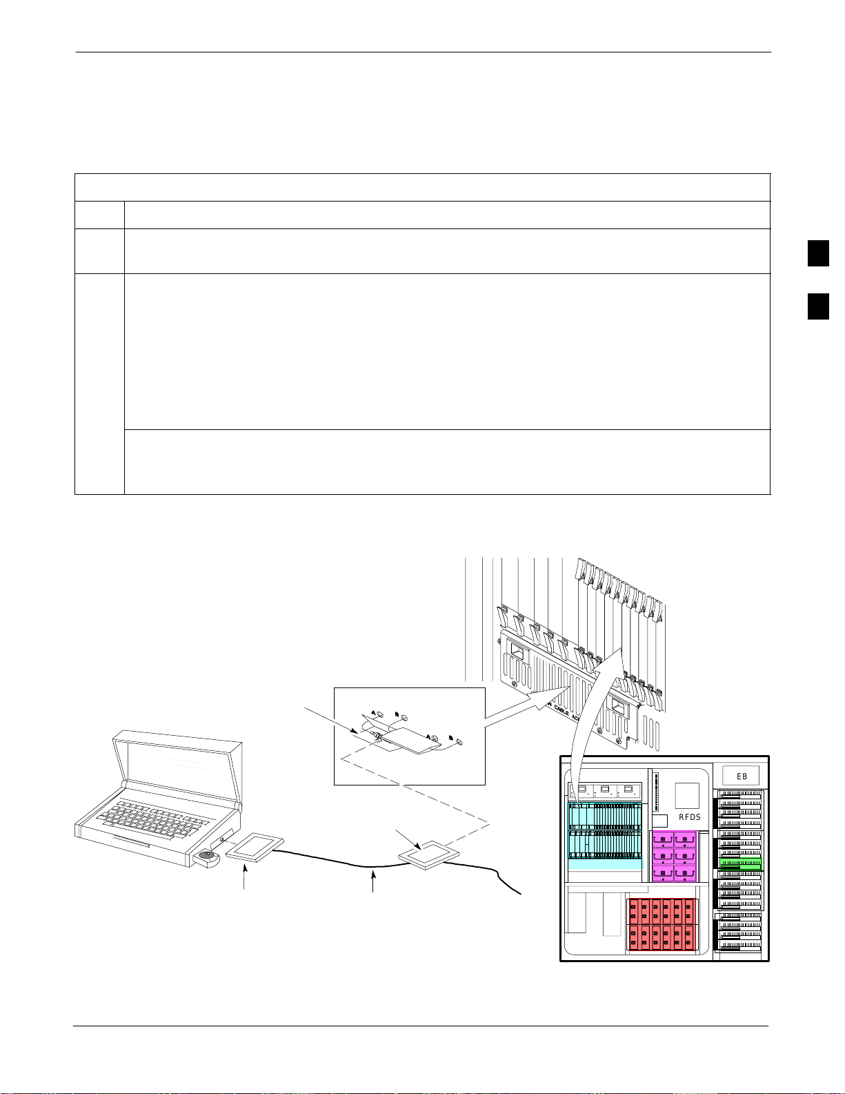
LMF Operation68P09255A57-2
LMF to BTS Connection
The LMF is connected to the LAN A or B connector located on the left
side of the frame’s lower air intake grill, behind the LAN Cable Access
door (see Figure 3-4).
Table 3-6: LMF to BTS Connection
Step Action
1 To gain access to the connectors, open the LAN Cable Access door, then pull apart the Velcro tape
covering the BNC “T” connector and slide out the computer service tray, if desired (see Figure 3-4).
2
Connect the LMF to the LAN A BNC connector via PCMCIA Ethernet Adapter with an unshielded
twisted-pair (UTP) Adapter and 10BaseT/10Base2 converter (powered by an external AC/DC
transformer). If there is no login response, connect the LMF to the LAN B BNC connector. If there is
still no login response, see Table 6-1, Login Failure Troubleshooting Procedure.
NOTE
- Xircom Model PE3-10B2 or equivalent can also be used to interface the LMF Ethernet
connection to the frame connected to the PC parallel port, powered by an external AC/DC
transformer. In this case, the BNC cable must not exceed 91 cm (3 ft) in length.
3
* IMPORTANT
The LAN shield is isolated from chassis ground. The LAN shield (exposed portion of BNC connector)
must not touch the chassis during optimization.
Figure 3-4: LMF Connection Detail
LMF BNC “T” CONNECTIONS
ON LEFT SIDE OF FRAME
(ETHERNET “A” SHOWN;
ETHERNET “B” COVERED
WITH VELCRO TAPE)
NOTE:
Open LAN CABLE ACCESS
door. Pull apart Velcro tape and
gain access to the LAN A or LAN
B LMF BNC connector.
10BASET/10BASE2
CONVERTER CONNECTS
DIRECTLY TO BNC T
ETIB
EBA
RFDS
LMF COMPUTER
TERMINAL WITH
MOUSE
Aug 2002
PCMCIA ETHERNET
ADPATER & ETHERNET
UTP ADAPTER
UNIVERSAL TWISTED
PAIR (UTP) CABLE (RJ11
CONNECTORS)
115 VAC POWER
CONNECTION
SC4812ET Optimization/ATP Manual Software Release R16.1.x.x
PRELIMINARY
SC4812ET RF CABINET
FW00168
3-19
Page 90

LMF Operation
Pinging the Processors
68P09255A57-2
For proper operation, the integrity of the Ethernet LAN A and B links
must be be verified. Figure 3-5 represents a typical BTS Ethernet
configuration. The drawing depicts one (of two identical) links, A and B.
Ping is a program that sends request packets to the LAN network
modules to get a response from the specified “target” module.
NOTE
WinLMF (unreleased version 2.16.1.0.15 for example) has an
option in the LOGIN menu to ping the GLI prior to login.
Follow the steps in Table 3-7 to ping each processor (on both LAN A
3
CAUTION
and LAN B) and verify LAN redundancy is working properly.
Always wear a conductive, high impedance wrist strap while
handling any circuit card/module to prevent damage by ESD.
Figure 3-5: BTS Ethernet LAN Interconnect Diagram
OUT
50Ω
SIGNAL
GROUND
GND
Lugs
CHASSIS
GROUND
50 Pair
Punch
Block
(Alarms/
Spans)
Spans
Alams
Modem
20 Pair
Punchblock
(RGPS)
RGD/RGPS
Micro-
wave
RF
GPS
LAN
IN OUT
A
B
19 MHz
2 Sec
RGD
Board
Power Input
+27V
Power Input
27V Ret
(MASTER)
1A 2A 3A 1B 2B 3B
4A 5A 6A 4B 5B 6B
RF Expansion Ports
1A 2A 3A 1B 2B 3B
Remote
ASU
4A 5A 6A 4B 5B 6B
1
2
BTS
Antenna’s
50Ω
SIGNAL
GROUND
GND
Lugs
50 Pair
Punch
Block
(Alarms/
Spans)
Spans
Alams
IN
Modem
20 Pair
Punchblock
(RGPS)
RGD/RGPS
Microwave
RF
GPS
LAN
IN OUT
A
B
19 MHz
2 Sec
RGD
Board
Power Input
+27V
Power Input
27V Ret
(EXPANSION)
1A 2A 3A 1B 2B 3B
4A 5A 6A 4B 5B 6B
RF Expansion Ports
1A 2A 3A 1B 2B 3B
Remote
ASU
4A 5A 6A 4B 5B 6B
1
2
BTS
Antenna’s
3-20
50Ω
SIGNAL
GROUND
NOTE
IMPORTANT: The Ethernet LAN A and B cables must be
installed on each frame/enclosure before performing this test. All
other processor board LAN connections are made via the
backplanes.
SC4812ET Optimization/ATP Manual Software Release R16.1.x.x
PRELIMINARY
50Ω
SIGNAL
GROUND
CHASSIS
GROUND
Aug 2002
FW00199
Page 91

LMF Operation68P09255A57-2
Table 3-7: Pinging the Processors
Step Action
1 From the Windows desktop, click the Start button and select Run.
2 In the Open box, type ping and the GLI IP address (for example, ping 128.0.0.2).
NOTE
128.0.0.2 is the default IP address for the GLI3 in field BTS units.
3 Click on the OK button.
4 If the targeted module responds, text similar to the following is displayed:
Reply from 128 128.0.0.2: bytes=32 time=3ms TTL=255
If there is no response the following is displayed:
Request timed out
If the GLI3 fails to respond, it should be reset and re-pinged. If it still fails to respond, typical
problems are shorted BNC to inter-frame cabling, open cables, crossed A and B link cables, or the
GLI3 itself.
Log into and out of the BTS
Table 3-8: Logging into the BTS
Step Action
NOTE
The LMF Mouse/Tracball must be attached if Windows and/or the GUI applications will be used.
1 Connect the LMF to the BTS as shown in .
2 Power-up the LMF. Allow the Windows operating system to come up.
3
3 Click the CDMA LMF desktop icon.
4 Click CDMA icon. Ths list of available BTS cell sites appears.
5 Click on the desired BTS (for example, BTS-6). If the IP Address and Port number are correct, press
Login to BTS.
6 To keep the current IP Address for the next log in, click the Remember Modified Address box (a
check appears in the box).
7 To use the default IP Address setting, click on Use Defaults.
Aug 2002
SC4812ET Optimization/ATP Manual Software Release R16.1.x.x
PRELIMINARY
3-21
Page 92

Download Files to the LMF - Site Specific BTS Files
Download Files to the LMF - Site Specific BTS Files
These procedures must be followed prior to an initial BTS optimization,
or anytime a new release of the BTS operating system software is to be
loaded from the LMF to the BTS.
Follow the steps outlined in Table 3-9 to create a bts directory and
download files to that bts-specific directory. Perform this procedure only
if the CDF files have not been previously loaded.
Table 3-9: Downloading Site Specific BTS Files
68P09255A57-2
3
Step Action
NOTE
The types of files that can be downloaded include calibration files (.cal extension) and CDF files
(.cdf extension). Files may be compressed (indicated by a .Z extension).
1 Obtain the 3.5-in. diskette(s) containing the configuration data file and calibration data.
2 Enter the following UNIX command from the /usr/lmf directory, to create a BTS specific
directory (if it does not already exist).
mkdir bts-<bts#>
3 Enter the following UNIX command to change to the newly created directory:
cd bts-<bts#>
4 Insert the first 3.5 inch floppy diskette. Verify disk is loaded with the proper BTS files/ versions by
typing the following at the
seedisk <cr>
5 To load the BTS files from the disk into the appropriate directory, enter the following at the (lmf):
prompt:
fromdisk <cr>
(lmf): prompt:
NOTE
Copy bts-#.cdf and (if they exist) bts-#.cal files to the /usr/lmf/bts-# directory. (# equates
to the actual BTS site number).
Unless sites use different device loads, create links to device files (as described in Table 3-10)
rather than placing individual copies into each bts directory.
6 If files are compressed, use the uncompress *.Z command to unpack files.
Download Files to the LMF - Master-bts-cdma Files
These procedures must be followed prior to an initial BTS optimization,
or anytime a new release of the BTS operating system software is to be
loaded from the LMF to the BTS.
Follow the steps outlined in Table 3-10 to create a bts-master-cdma
directory, to download files, and to create softlinks to the device load
bts- <bts#> subdirectory. (Always consult
3-22
files into the appropriate
latest software release notes as this is an interim procedure and is subject
to change).
SC4812ET Optimization/ATP Manual Software Release R16.1.x.x
PRELIMINARY
Aug 2002
Page 93

Download Files to the LMF - Site Specific BTS Files68P09255A57-2
Table 3-10: Downloading and linking master-bts-cdma directory files for device loads
Step Action
NOTE
If the current LMF code needs to be installed on the LMF PC, or if more information on file
management, creating bts directories, or viewing CDF files is needed, refer to the.LMF Users
Guide.
The types of files that can be downloaded include code (.hex or .bin extension) and data (.dds
extension) files. Files may be compressed (indicated by a .Z extension).
1 Enter the following UNIX command, from the /usr/lmf directory, to create a device load master
directory (if it does not already exist).
mkdir bts-master-cdma
2 Enter the following UNIX command to change to the newly created directory:
cd bts-master-cdma
3 Obtain the 3.5-in. diskette(s) containing the current release of the BTS operating code and/or data
files.
NOTE
File naming conventions for all processor boards and applicable files for each are listed below.
Rename files using the
Device File Name(s)
mv UNIX command as required:
3
GLI <version>-gliboot.hex & gli.dds
BBX <version>-bbxboot.hex & bbx.dds
BDC <version>-bdcboot.hex & bdc.dds
MCC <version>-mccboot.hex.0501 & mcc.dds.0501
CSM <version>-csmboot.hex & csm.dds
TSU tsuboot.hex
4 Insert the first 3.5 inch floppy diskette. Verify disk is loaded with the proper BTS files/versions by
typing the following at the
seedisk <cr>
5 To load the BTS files from the disk into the appropriate directory, enter the following at the (lmf):
prompt:
fromdisk <cr>
6 If files are compressed, use the uncompress *.Z command to unpack files. Rename files to match
the naming conventions listed above if required.
7 Repeat Steps 4 and 5 for each diskette that is a part of this load.
(lmf): prompt:
NOTE
All older versions of files (and links to files) in the bts-master- bts-<bts#> subdirectories must
be removed before beginning this procedure.
. . . continued on next page
Aug 2002
SC4812ET Optimization/ATP Manual Software Release R16.1.x.x
PRELIMINARY
3-23
Page 94

Download Files to the LMF - Site Specific BTS Files
68P09255A57-2
Table 3-10: Downloading and linking master-bts-cdma directory files for device loads
Step Action
8 Create softlinks to the device load and data load files in the bts-master-cdma directory using the
following UNIX commands:
ln -s /usr/lmf/bts-master-cdma/*.hex /usr/lmf/bts-<bts#>/
ln -s /usr/lmf/bts-master-cdma/*.hex.* /usr/lmf/bts-<bts#>/
ln -s /usr/lmf/bts-master-cdma/*.dds /usr/lmf/bts-<bts#>/
ln -s /usr/lmf/bts-master-cdma/*.dds.* /usr/lmf/bts-<bts#>/
3
NOTE
You may need to specify specific file names in the command instead of using the * ”wildcard”
character in order to link multiple versions of files in the same subdirectory. Using *.* will link ALL
files in the directory.
3-24
SC4812ET Optimization/ATP Manual Software Release R16.1.x.x
PRELIMINARY
Aug 2002
Page 95

Download Files to the LMF - Site Specific BTS Files68P09255A57-2
Create BTS Specific CDF File
Follow the steps outlined in Table 3-11 to create a BTS specific CDF
file, if one cannot be obtained from the OMCR/CBSC. (This is an
interim procedure and is subject to change).
Table 3-11: Create BTS Specific CDF File
Step Action
! CAUTION
If you are not familiar with the UNIX vi editor, create a “dummy” CDF file, and practice making
changes to it, prior to altering the “real” one.
NOTE
For more information on file management, creating bts directories, viewing/editing CDF files, refer
to LMF Users Guide.
1 Determine the CDF file, currently loaded on the LMF, is closest to the configuration at the site. Use a
generic CDF file that equips all devices, if possible. If this is an OMNI site, use an OMNI CDF file,
if SECTOR, use SECTOR CDF file.
2
List the contents of the bts-<bts#> directory by entering the ls command at the (lmf) prompt
followed by a <cr>, to verify the CDF file for the site does not already exist.
3
3
Enter the following command to copy an existing CDF file on the LMF hard drive to the new BTS
directory.
cp /usr/lmf/bts-src_<bts#>.cdf /usr/lmf/bts- dest_<bts#>.cdf
NOTE
The following step is for LMF software releases version 5 and 6 only.
Globally change the BTS ID in the new CDF file using the following UNIX commands:
4
vi bts-new_<bts#>.cdf
:1,$ s/Id1 = old_<bts#>/Id1 = new_<bts#>
:1,$ s/old_<bts#>_/new_<bts#>_
Include the underscore after the old and new bts # in the above command
:1,$ s/BTS\[old_<bts#>/BTS\[new_<bts#>
:wq
NOTE
You should now be able to log into the bts using the new CDF file. If you search for the old BTS #, it
should be gone. You will have to edit the CDF file (using the vi editor) as far as BBX, MCC, etc.
equipage is concerned.
Update BTS Specific CDF File Device Load Version and Site Type
Follow the steps outlined in Table 3-12 to update the existing BTS
specific CDF file NextLoad parameter, to reflect the current device load
version to be downloaded and verify the correct Site Type. (This is an
interim procedure and is subject to change).
Aug 2002
CAUTION
SC4812ET Optimization/ATP Manual Software Release R16.1.x.x
Device load version in the CDF file must match the current
version loaded at the OMCR/CBSC.
PRELIMINARY
3-25
Page 96

Download Files to the LMF - Site Specific BTS Files
68P09255A57-2
Table 3-12: Update BTS Specific CDF File Device Load Version
Step Action
! CAUTION
If you are not familiar with the UNIX vi editor, create a “dummy” CDF file, and practice making
changes to it, prior to altering the “real” one.
* IMPORTANT
CDF files obtained from the OMCR/CBSC are modified by DELTA information being appended to
the end of the CDF file. The information in the DELTA fields take precedence over information in the
“core CDF file” For example: If NextLoad=‘‘1.2.3.4.5” for BBX 1 was specified in the CDF file, and
3
there was a DELTA entry specifying NextLoad=‘‘2.3.4.5.6” appended to the CDF file for the same
BBX, 2.3.4.5.6 would be the version used.
There are two ways resolve this. Edit both the DELTA and “core” areas of the file to reflect the same
version, or make sure the delta information is transferred to the main CDF file and delete all DELTA
CDF file entries.
1 Globally change the device load version number in the new CDF file using the following UNIX
commands:
vi bts-new_<bts#>.cdf
:1,$ s/x.x.x.x.x/y.y.y.y.y
Where: x.x.x.x.x and y.y.y.y.y represent the old and new version number, respectively.
:wq
NOTE
You should now be able to download all devices at the BTS with the current device load version.
2 Verify the SiteType and SSType entries in the CDF file (under the BTS subheading) reflect the
following information. See example of applicable fields of CDF file below.
(CDMA only; 1900 MHz example shown):
BTS[#] = {
....,
SiteType=3,
SSType=16
...
},
Valid SiteTypes(SC9600=1, SC9600(Mixed)=2, SC2400=3, SC2400(Mixed)=4, SC600=5)
Valid SSTypes (CDMA800MHz=8, CDMA1900MHz=16, CDMA900MHz=32)
Update Antenna Mapping Files
Earlier release versions may require the antenna.map file to be
updated. There are two antenna mapping files. These are
antenna.map and antenna.asu.
3-26
Follow the steps outlined in Table 3-13 to check the antenna mapping
file and update as needed.
SC4812ET Optimization/ATP Manual Software Release R16.1.x.x
PRELIMINARY
Aug 2002
Page 97

Download Files to the LMF - Site Specific BTS Files68P09255A57-2
Table 3-13: Update Antenna Mapping Files
Step Action
! CAUTION
If you are not familiar with the UNIX vi editor, create a “dummy” CDF file, and practice making
changes to it, prior to altering the “real” one.
NOTE
For more information on file management, creating bts directories, viewing/editing CDF files, refer to
the LMF Users Guide.
1 View the antenna.map file (see below) and verify the Xcvrs listed in the CDF file (and that are
equipped in the BTS) are also listed in the antenna.map file (for both RX and TX tables). Make
sure the antenna.map file has enough RX and TX antennas listed to cover the number of sectors
indicated by CDF’s SiteConf parameter.
Example of Antenna Map File
R --- Rx --- -- Sec -- ----- Xcvrs ----R 1:M :RX1: 1 :1,4,5,8
R 2:D :RX2: 1 :1,4,5,8
R 3:M :RX3: 2 :2,4,6,8
R 4:D :RX4: 2 :2,4,6,8
R 5:M :RX5: 3 :3,4,7,8
R 6:D :RX6: 3 :3,4,7,8
T --- Tx --- -- Sec -- ----- Xcvrs ----T 1:0 :TX1: 1 :1,4
T 2:0 :TX2: 2 :2,4
T 3:0 :TX3: 3 :3,4
T 4:0 :TX4: 1 :5,8
T 5:0 :TX5: 2 :6,8
T 6:0 :TX6: 3 :7,8
2 Verify all RX and TX antennas listed in the file antenna.map are also listed in the antenna.asu
file.
NOTE
The antenna.asu file is required only if the BTS is equipped with RFDS. Be sure that the information
in antenna files matches your actual configuration.
3
Aug 2002
SC4812ET Optimization/ATP Manual Software Release R16.1.x.x
PRELIMINARY
3-27
Page 98

Operating the LMF
Operating the LMF
Basic Operation
68P09255A57-2
NOTE
The CDMA LMF allows the user to work in the two following operating
environments which are accessed using the specified desktop icon:
The terms “CDMA LMF” and “WinLMF” are interchangeable
Graphical User Interface (GUI) using the WinLMF icon
Command Line Interface (CLI) using the WinLMF CLI icon
3
The GUI is the primary optimization and acceptance testing operating
environment. The CLI environment provides additional capability to the
user to perform manually controlled acceptance tests and audit the
results of optimization and calibration actions.
Basic operation of the LMF GUI includes the following:
Selecting and deselecting BTS devices
Enabling devices
Disabling devices
Resetting devices
Obtaining device status
Sorting a status report window
For detailed information on performing these and other LMF operations,
refer to the CDMA LMF Operator’s Guide, 68P64114A78.
Both the GUI and the CLI use a program known as the handler. Only one
handler can be running at one time. The architectural design is such that
the GUI must be started before the CLI if you want the GUI and CLI to
use the same handler.
When the CLI is launched after the GUI, the CLI automatically finds and
uses an in-progress login session with a BTS initiated under the GUI.
This allows the use of the GUI and the CLI in the same BTS login
session.
If a CLI handler is already running when the GUI is launched (this
happens if the CLI window is already running when the user starts the
GUI, or if another copy of the GUI is already running when the user
starts the GUI), a dialog window displays the following warning
message:
The CLI handler is already running.
This may cause conflicts with the LMF.
Are you sure that you want to start the application?
This window also contains yes and no buttons. Selecting yes starts the
application. Selecting no terminates the application.
3-28
SC4812ET Optimization/ATP Manual Software Release R16.1.x.x
PRELIMINARY
Aug 2002
Page 99

Operating the LMF68P09255A57-2
CLI Format Conventions
The CLI command can be broken down in the following way:
Verb
Device including device identifier parameters
Switch
Option parameters consisting of:
- Keywords
- Equals sign (=) between the keyword and the parameter value
- Parameter values
Spaces are required between the verb, device, switch, and option
parameters. A hyphen is required between the device and its identifiers.
Following is an example of a CLI command.
measure bbx-<bts_id>-<bbx_id> rssi channel=6 sector=5
Refer to the LMF CLI Commands (68P09251A59) for a complete
explanation of the CLI commands and their usage.
3
Logging into a BTS
NOTE
Be sure that the correct bts-#.cdf and cbsc-#.cdf file is used for
the BTS. These should be the CDF files that are provided for the
BTS by the CBSC. Failure to use the correct CDF files can
result in wrong results. Failure to use the correct CDF files to
log into a live (traffic carrying) site can shut down the site.
Logging into a BTS establishes a communications link between the BTS
and the CDMA LMF. You may be logged into one or more BTS’s at a
time, but only one LMF may be logged into each BTS.
Before attempting to log into the BTS, confirm the CDMA LMF is
properly connected to the BTS (see Figure 3-4). Follow the procedure in
Table 3-14 to log into a BTS.
Prerequisites
Before attempting to login to a BTS, ensure the following have been
completed:
The LMF is correctly installed and prepared.
A bts-nnn folder with the correct CDF and CBSC file exists.
The LMF is correctly installed and prepared, and the LMF computer
was connected to the BTS before starting the Windows operating
system and LMF software. If necessary, restart the computer after
connecting it to the BTS (see Table 3-6 and Figure 3-4).
Aug 2002
BTS Login from the GUI Environment
Follow the procedures in Table 3-14 to log into a BTS when using the
GUI environment
SC4812ET Optimization/ATP Manual Software Release R16.1.x.x
PRELIMINARY
3-29
Page 100

Operating the LMF
Table 3-14: BTS GUI Login Procedure
Step Action
1 Start the LMF GUI environment by double clicking on the WinLMF desktop icon (if the LMF’s not
running).
68P09255A57-2
NOTE
If a warning similar to the following is displayed, select No, shut down other LMF sessions which
may be running, and start the LMF GUI environment again:
The CLI handler is already running.
This may cause conflicts with the LMF
3
Are you sure you want to start the application?
Yes No
2 Click on Login tab (if not displayed).
3 If no base stations are displayed in the Available Base Stations pick list, double click on the CDMA
icon.
4 Click on the desired BTS number.
5 Click on the Network Login tab (if not already in the forefront).
6 Enter correct IP address (normally 128.0.0.2 for a field BTS) if not correctly displayed in the IP
Address box.
NOTE
128.0.0.2 is the default IP address for MGLI-1 in field BTS units. 128.0.0.1 is the default IP address
for MGLI-2.
7 Type in the correct IP Port number (normally 9216) if not correctly displayed in the IP Port box.
8 Select the Multi-channel Preselector type from the Multi-channel Preselector drop-down list (default
is MPC) to a device corresponding to your BTS configuration if required.
NOTE
When performing RX tests on expansion frames, do not choose EMPC if the test equipment is
connected to the starter frame.
9 Click on the Use a Tower Top Amplifier, if applicable.
Click on Login. (A BTS tab with the BTS is displayed.)
10
NOTE
If you attempt to log in to a BTS that is already logged on, all devices will be gray.
There may be instances where the BTS initiates a log out due to a system error (i.e., a device
failure).
If the MGLI is OOS_ROM (blue), it will have to be downloaded with code before other devices can
be seen.
If the MGLI is OOS-RAM (yellow), it must be enabled before other installed devices can be seen.
3-30
BTS Login from the CLI Environment
Follow the procedures in Table 3-15 to log into a BTS when using the
GUI environment
SC4812ET Optimization/ATP Manual Software Release R16.1.x.x
PRELIMINARY
Aug 2002
 Loading...