

Page 1

Nokia Customer Care
Service Manual
RM-497 (Nokia 7020)
Mobile Terminal
Part No: (Issue 1)
COMPANY CONFIDENTIAL
Copyright © 2010 Nokia. All rights reserved.
Page 2

Amendment Record Sheet
Amendment Record Sheet
Amendment No Date Inserted By Comments
Original issue 10/2010 Jeff Zhao
RM-497
Page ii COMPANY CONFIDENTIAL Issue 1
Copyright © 2010 Nokia. All rights reserved.
Page 3

RM-497
Copyright
Copyright
Copyright © 2010 Nokia. All rights reserved.
Reproduction, transfer, distribution or storage of part or all of the contents in this document in any form
without the prior written permission of Nokia is prohibited.
Nokia, Nokia Connecting People, and Nokia X and Y are trademarks or registered trademarks of Nokia
Corporation. Other product and company names mentioned herein may be trademarks or tradenames of
their respective owners.
Nokia operates a policy of continuous development. Nokia reserves the right to make changes and
improvements to any of the products described in this document without prior notice.
Under no circumstances shall Nokia be responsible for any loss of data or income or any special, incidental,
consequential or indirect damages howsoever caused.
The contents of this document are provided "as is". Except as required by applicable law, no warranties of
any kind, either express or implied, including, but not limited to, the implied warranties of merchantability
and fitness for a particular purpose, are made in relation to the accuracy, reliability or contents of this
document. Nokia reserves the right to revise this document or withdraw it at any time without prior notice.
The availability of particular products may vary by region.
IMPORTANT
This document is intended for use by qualified service personnel only.
Issue 1 COMPANY CONFIDENTIAL Page iii
Copyright © 2010 Nokia. All rights reserved.
Page 4

RM-497
Warnings and cautions
Warnings and cautions
Warnings
•
IF THE DEVICE CAN BE INSTALLED IN A VEHICLE, CARE MUST BE TAKEN ON INSTALLATION IN VEHICLES FITTED
WITH ELECTRONIC ENGINE MANAGEMENT SYSTEMS AND ANTI-SKID BRAKING SYSTEMS. UNDER CERTAIN FAULT
CONDITIONS, EMITTED RF ENERGY CAN AFFECT THEIR OPERATION. IF NECESSARY, CONSULT THE VEHICLE DEALER/
MANUFACTURER TO DETERMINE THE IMMUNITY OF VEHICLE ELECTRONIC SYSTEMS TO RF ENERGY.
•
THE PRODUCT MUST NOT BE OPERATED IN AREAS LIKELY TO CONTAIN POTENTIALLY EXPLOSIVE ATMOSPHERES,
FOR EXAMPLE, PETROL STATIONS (SERVICE STATIONS), BLASTING AREAS ETC.
•
OPERATION OF ANY RADIO TRANSMITTING EQUIPMENT, INCLUDING CELLULAR TELEPHONES, MAY INTERFERE
WITH THE FUNCTIONALITY OF INADEQUATELY PROTECTED MEDICAL DEVICES. CONSULT A PHYSICIAN OR THE
MANUFACTURER OF THE MEDICAL DEVICE IF YOU HAVE ANY QUESTIONS. OTHER ELECTRONIC EQUIPMENT MAY
ALSO BE SUBJECT TO INTERFERENCE.
•
BEFORE MAKING ANY TEST CONNECTIONS, MAKE SURE YOU HAVE SWITCHED OFF ALL EQUIPMENT.
Cautions
•
Servicing and alignment must be undertaken by qualified personnel only.
•
Ensure all work is carried out at an anti-static workstation and that an anti-static wrist strap is worn.
•
Ensure solder, wire, or foreign matter does not enter the telephone as damage may result.
•
Use only approved components as specified in the parts list.
•
Ensure all components, modules, screws and insulators are correctly re-fitted after servicing and
alignment.
•
Ensure all cables and wires are repositioned correctly.
•
Never test a mobile phone WCDMA transmitter with full Tx power, if there is no possibility to perform the
measurements in a good performance RF-shielded room. Even low power WCDMA transmitters may disturb
nearby WCDMA networks and cause problems to 3G cellular phone communication in a wide area.
•
During testing never activate the GSM or WCDMA transmitter without a proper antenna load, otherwise
GSM or WCDMA PA may be damaged.
Page iv COMPANY CONFIDENTIAL Issue 1
Copyright © 2010 Nokia. All rights reserved.
Page 5

RM-497
For your safety
For your safety
QUALIFIED SERVICE
Only qualified personnel may install or repair phone equipment.
ACCESSORIES AND BATTERIES
Use only approved accessories and batteries. Do not connect incompatible products.
CONNECTING TO OTHER DEVICES
When connecting to any other device, read its user’s guide for detailed safety instructions. Do not connect
incompatible products.
Issue 1 COMPANY CONFIDENTIAL Page v
Copyright © 2010 Nokia. All rights reserved.
Page 6

RM-497
Care and maintenance
Care and maintenance
This product is of superior design and craftsmanship and should be treated with care. The suggestions below
will help you to fulfil any warranty obligations and to enjoy this product for many years.
•
Keep the phone and all its parts and accessories out of the reach of small children.
•
Keep the phone dry. Precipitation, humidity and all types of liquids or moisture can contain minerals that
will corrode electronic circuits.
•
Do not use or store the phone in dusty, dirty areas. Its moving parts can be damaged.
•
Do not store the phone in hot areas. High temperatures can shorten the life of electronic devices, damage
batteries, and warp or melt certain plastics.
•
Do not store the phone in cold areas. When it warms up (to its normal temperature), moisture can form
inside, which may damage electronic circuit boards.
•
Do not drop, knock or shake the phone. Rough handling can break internal circuit boards.
•
Do not use harsh chemicals, cleaning solvents, or strong detergents to clean the phone.
•
Do not paint the phone. Paint can clog the moving parts and prevent proper operation.
•
Use only the supplied or an approved replacement antenna. Unauthorised antennas, modifications or
attachments could damage the phone and may violate regulations governing radio devices.
All of the above suggestions apply equally to the product, battery, charger or any accessory.
Page vi COMPANY CONFIDENTIAL Issue 1
Copyright © 2010 Nokia. All rights reserved.
Page 7

RM-497
ESD protection
ESD protection
Nokia requires that service points have sufficient ESD protection (against static electricity) when servicing
the phone.
Any product of which the covers are removed must be handled with ESD protection. The SIM card can be
replaced without ESD protection if the product is otherwise ready for use.
To replace the covers ESD protection must be applied.
All electronic parts of the product are susceptible to ESD. Resistors, too, can be damaged by static electricity
discharge.
All ESD sensitive parts must be packed in metallized protective bags during shipping and handling outside
any ESD Protected Area (EPA).
Every repair action involving opening the product or handling the product components must be done under
ESD protection.
ESD protected spare part packages MUST NOT be opened/closed out of an ESD Protected Area.
For more information and local requirements about ESD protection and ESD Protected Area, contact your local
Nokia After Market Services representative.
Issue 1 COMPANY CONFIDENTIAL Page vii
Copyright © 2010 Nokia. All rights reserved.
Page 8

RM-497
Battery information
Battery information
Note: A new battery's full performance is achieved only after two or three complete charge and
discharge cycles!
The battery can be charged and discharged hundreds of times but it will eventually wear out. When the
operating time (talk-time and standby time) is noticeably shorter than normal, it is time to buy a new battery.
Use only batteries approved by the phone manufacturer and recharge the battery only with the chargers
approved by the manufacturer. Unplug the charger when not in use. Do not leave the battery connected to
a charger for longer than a week, since overcharging may shorten its lifetime. If left unused a fully charged
battery will discharge itself over time.
Temperature extremes can affect the ability of your battery to charge.
For good operation times with Ni-Cd/NiMh batteries, discharge the battery from time to time by leaving the
product switched on until it turns itself off (or by using the battery discharge facility of any approved accessory
available for the product). Do not attempt to discharge the battery by any other means.
Use the battery only for its intended purpose.
Never use any charger or battery which is damaged.
Do not short-circuit the battery. Accidental short-circuiting can occur when a metallic object (coin, clip or
pen) causes direct connection of the + and - terminals of the battery (metal strips on the battery) for example
when you carry a spare battery in your pocket or purse. Short-circuiting the terminals may damage the battery
or the connecting object.
Leaving the battery in hot or cold places, such as in a closed car in summer or winter conditions, will reduce
the capacity and lifetime of the battery. Always try to keep the battery between 15°C and 25°C (59°F and 77°
F). A phone with a hot or cold battery may temporarily not work, even when the battery is fully charged.
Batteries' performance is particularly limited in temperatures well below freezing.
Do not dispose of batteries in a fire!
Dispose of batteries according to local regulations (e.g. recycling). Do not dispose as household waste.
Page viii COMPANY CONFIDENTIAL Issue 1
Copyright © 2010 Nokia. All rights reserved.
Page 9

RM-497
Company policy
Company policy
Our policy is of continuous development; details of all technical modifications will be included with service
bulletins.
While every endeavour has been made to ensure the accuracy of this document, some errors may exist. If
any errors are found by the reader, NOKIA MOBILE PHONES Business Group should be notified in writing/email.
Please state:
•
Title of the Document + Issue Number/Date of publication
•
Latest Amendment Number (if applicable)
•
Page(s) and/or Figure(s) in error
Please send to:
NOKIA CORPORATION
Nokia Mobile Phones Business Group
Nokia Customer Care
PO Box 86
FIN-24101 SALO
Finland
E-mail: Service.Manuals@nokia.com
Issue 1 COMPANY CONFIDENTIAL Page ix
Copyright © 2010 Nokia. All rights reserved.
Page 10

RM-497
Company policy
(This page left intentionally blank.)
Page x COMPANY CONFIDENTIAL Issue 1
Copyright © 2010 Nokia. All rights reserved.
Page 11

RM-497
Nokia 7020 Service Manual Structure
Nokia 7020 Service Manual Structure
1 General information
2 Service Devices and Service Concepts
3 BB Troubleshooting and Manual Tuning Guide
4 RF troubleshooting
5 System Module
6 BTHFMTXRDS3.0b
Glossary
Issue 1 COMPANY CONFIDENTIAL Page xi
Copyright © 2010 Nokia. All rights reserved.
Page 12

RM-497
Nokia 7020 Service Manual Structure
(This page left intentionally blank.)
Page xii COMPANY CONFIDENTIAL Issue 1
Copyright © 2010 Nokia. All rights reserved.
Page 13

Nokia Customer Care
1 — General information
Issue 1 COMPANY CONFIDENTIAL Page 1 – 1
Copyright © 2010 Nokia. All rights reserved.
Page 14

RM-497
General information
(This page left intentionally blank.)
Page 1 – 2 COMPANY CONFIDENTIAL Issue 1
Copyright © 2010 Nokia. All rights reserved.
Page 15

RM-497
General information
Table of Contents
Product selection................................................................................................................................................... 1–5
Phone features ...................................................................................................................................................... 1–5
Accessories............................................................................................................................................................. 1–6
Technical specifications........................................................................................................................................ 1–6
General specifications...................................................................................................................................... 1–6
Battery Endurance............................................................................................................................................ 1–6
List of Figures
Figure 1 RM-497 (Nokia 7020) product picture.................................................................................................. 1–5
Issue 1 COMPANY CONFIDENTIAL Page 1 – 3
Copyright © 2010 Nokia. All rights reserved.
Page 16

RM-497
General information
(This page left intentionally blank.)
Page 1 – 4 COMPANY CONFIDENTIAL Issue 1
Copyright © 2010 Nokia. All rights reserved.
Page 17
RM-497
General information
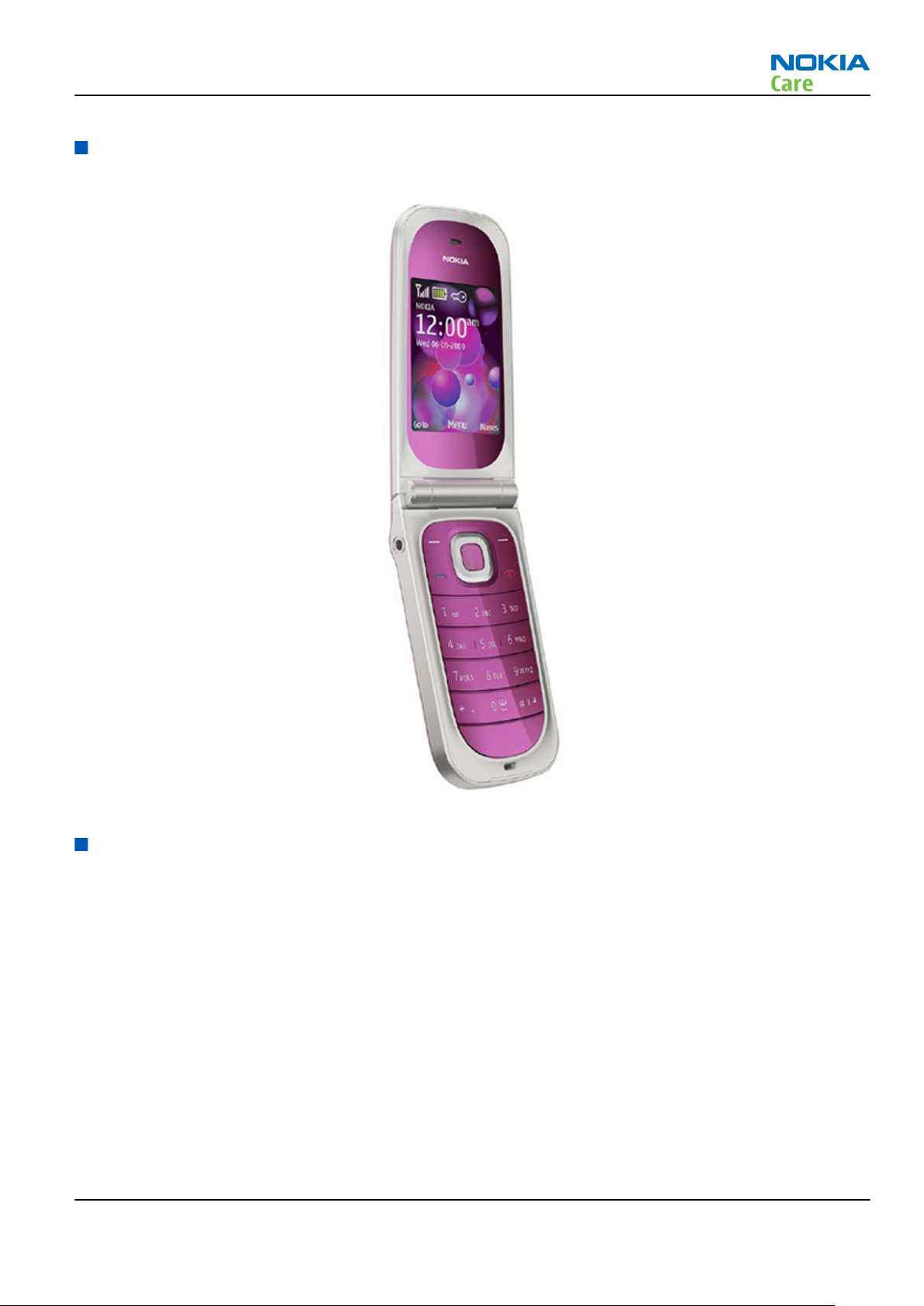
Product selection
RM-497 (Nokia 7020) is a GSM Quad-band phone, supporting EGSM 850/900/1800/1900 bands.
Figure 1 RM-497 (Nokia 7020) product picture
Phone features
Key features
•
S40, 6th Edition
•
Secondary display
•
Supporting quad-band GSM 850/900/1800/1900
•
Including Nokia Maps
•
2Mpix Camera
•
Bluetooth 2.1 + EDR
•
MIDP Java 2.1
•
microSD memory card slot (up to 16 GB)
•
High-Speed 2.0 Micro-USB connector
•
2.5 mm Nokia AV connector
•
Vibra
Issue 1 COMPANY CONFIDENTIAL Page 1 – 5
Copyright © 2010 Nokia. All rights reserved.
Page 18
•
Active standby
•
Display (size in cm, mm): 2.2"
•
No stereo speaker
•
No automatic lighting adjustment
Accessories
Sales package contents:
•
Transceiver: Nokia 7020
•
Battery: BL-4S
•
Charger: AC-3
•
Wired headset: WH-101
•
Data cable with USB: No (Yes for LTA)
•
Memory card: Yes, 2GB
•
CD-rom: No
•
User Guide: Yes
For out-box accessories, please refer to enhancement list document.
RM-497
General information
Technical specifications
General specifications
Unit Dimension (mm) Weight (g) Volume (cc)
Transceiver with BL-4S
battery pack
91.2 x 46.7 x 17.3 86.2 64.5
Battery Endurance
Battery Talk Time Standby Time Browsing time Music playing
BL-4S standard
battery
Note: Variation in operation time will occur depending on SIM card, network settings and usage.
Talk time is increased by up to 30% if half rate is active and reduced by 5% if enhanced full rate is
active.
4 hours and 36
minutes (GSM)
Up to 360
hours
(GSM)
350 minutes Up to 20 hours
and 10
minutes
time
Video playback
time
Up to 7 hours
and 5 minutes
Page 1 – 6 COMPANY CONFIDENTIAL Issue 1
Copyright © 2010 Nokia. All rights reserved.
Page 19

Nokia Customer Care
2 — Service Devices and
Service Concepts
Issue 1 COMPANY CONFIDENTIAL Page 2 – 1
Copyright © 2010 Nokia. All rights reserved.
Page 20

RM-497
Service Devices and Service Concepts
(This page left intentionally blank.)
Page 2 – 2 COMPANY CONFIDENTIAL Issue 1
Copyright © 2010 Nokia. All rights reserved.
Page 21

RM-497
Service Devices and Service Concepts
Table of Contents
Service devices....................................................................................................................................................... 2–5
Product specific devices................................................................................................................................... 2–5
MJ-224 .......................................................................................................................................................... 2–5
General devices................................................................................................................................................. 2–5
CU-4............................................................................................................................................................... 2–6
FLS-5 ............................................................................................................................................................. 2–7
FPS-21........................................................................................................................................................... 2–7
PK-1............................................................................................................................................................... 2–8
RJ-230 ........................................................................................................................................................... 2–8
SRT-6............................................................................................................................................................. 2–8
SS-34............................................................................................................................................................. 2–8
SS-93............................................................................................................................................................. 2–8
SX-4............................................................................................................................................................... 2–9
Cables................................................................................................................................................................. 2–9
CA-101 .......................................................................................................................................................... 2–9
PCS-1............................................................................................................................................................. 2–9
XRS-6.......................................................................................................................................................... 2–10
Service concepts ................................................................................................................................................. 2–10
POS (Point of Sale) flash concept ................................................................................................................. 2–10
Basic flash concept L3................................................................................................................................... 2–11
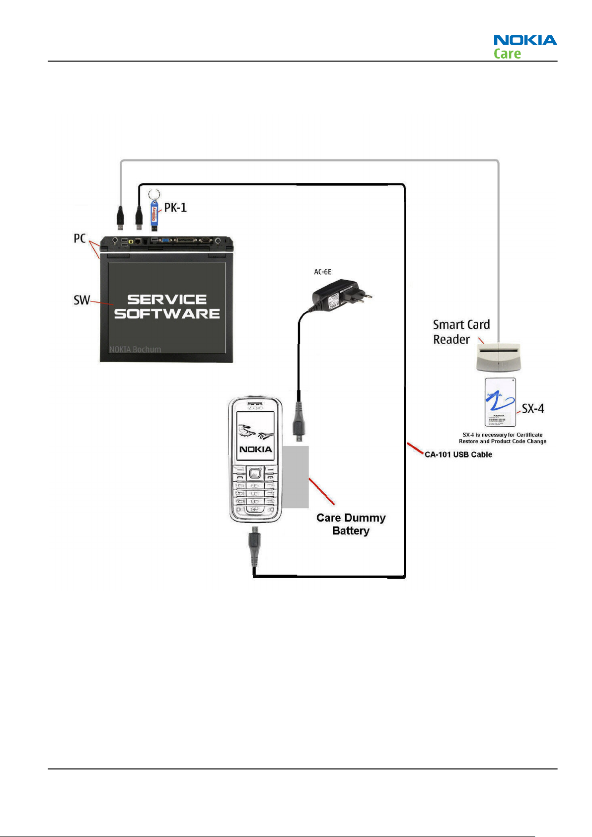
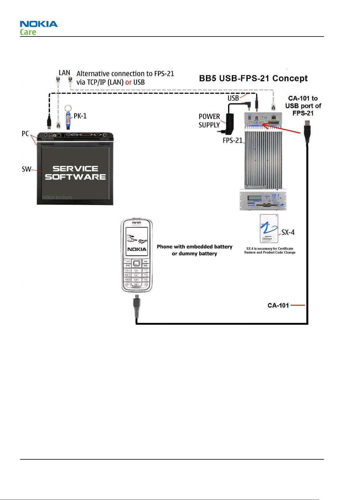
Flash concept with FPS-21............................................................................................................................ 2–12
Basic BB tune concept (EM calibration)....................................................................................................... 2–14
Basic RF&BB tune concept with FPS-21....................................................................................................... 2–15
List of Figures
Figure 2 POS flash concept ................................................................................................................................ 2–10
Figure 3 Basic flash concept L3 ......................................................................................................................... 2–11
Figure 4 Flash concept with FPS-21 (A)............................................................................................................ 2–12
Figure 5 Flash concept with FPS-21 (B)............................................................................................................ 2–13
Figure 6 Basic BB tune concept (EM calibration)............................................................................................. 2–14
Figure 7 Basic RF&BB tune concept with FPS-21 (A) ....................................................................................... 2–15
Figure 8 Basic RF&BB tune concept with FPS-21 (B) ....................................................................................... 2–16
Issue 1 COMPANY CONFIDENTIAL Page 2 – 3
Copyright © 2010 Nokia. All rights reserved.
Page 22

RM-497
Service Devices and Service Concepts
(This page left intentionally blank.)
Page 2 – 4 COMPANY CONFIDENTIAL Issue 1
Copyright © 2010 Nokia. All rights reserved.
Page 23
RM-497
Service Devices and Service Concepts
Service devices
Product specific devices
The table below gives a short overview of service devices that can be used for testing, error analysis, and
repair of product RM-497. For the correct use of the service devices, and the best effort of workbench setup,
please refer to various concepts.
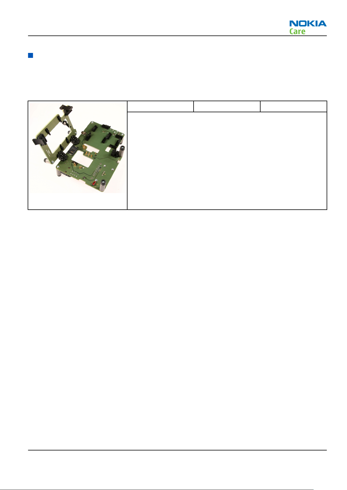
MJ-224 Module jig MJ-224 is meant for component level troubleshooting.
The jig includes an RF interface for GSM and Bluetooth. In addition, it
has the following features:
•
Provides mechanical interface with the engine module
•
Provides galvanic connection to all needed test pads in module
•
MMC interface
•
Duplicated SIM connector
•
Connector for control unit
•
Access for AV- and USB connectors
•
CA-128RS cable is used together with this jig for RF testing.
General devices
The table below gives a short overview of service devices that can be used for testing, error analysis, and
repair of product RM-497. For the correct use of the service devices, and the best effort of workbench setup,
please refer to various concepts.
Issue 1 COMPANY CONFIDENTIAL Page 2 – 5
Copyright © 2010 Nokia. All rights reserved.
Page 24
RM-497
Service Devices and Service Concepts
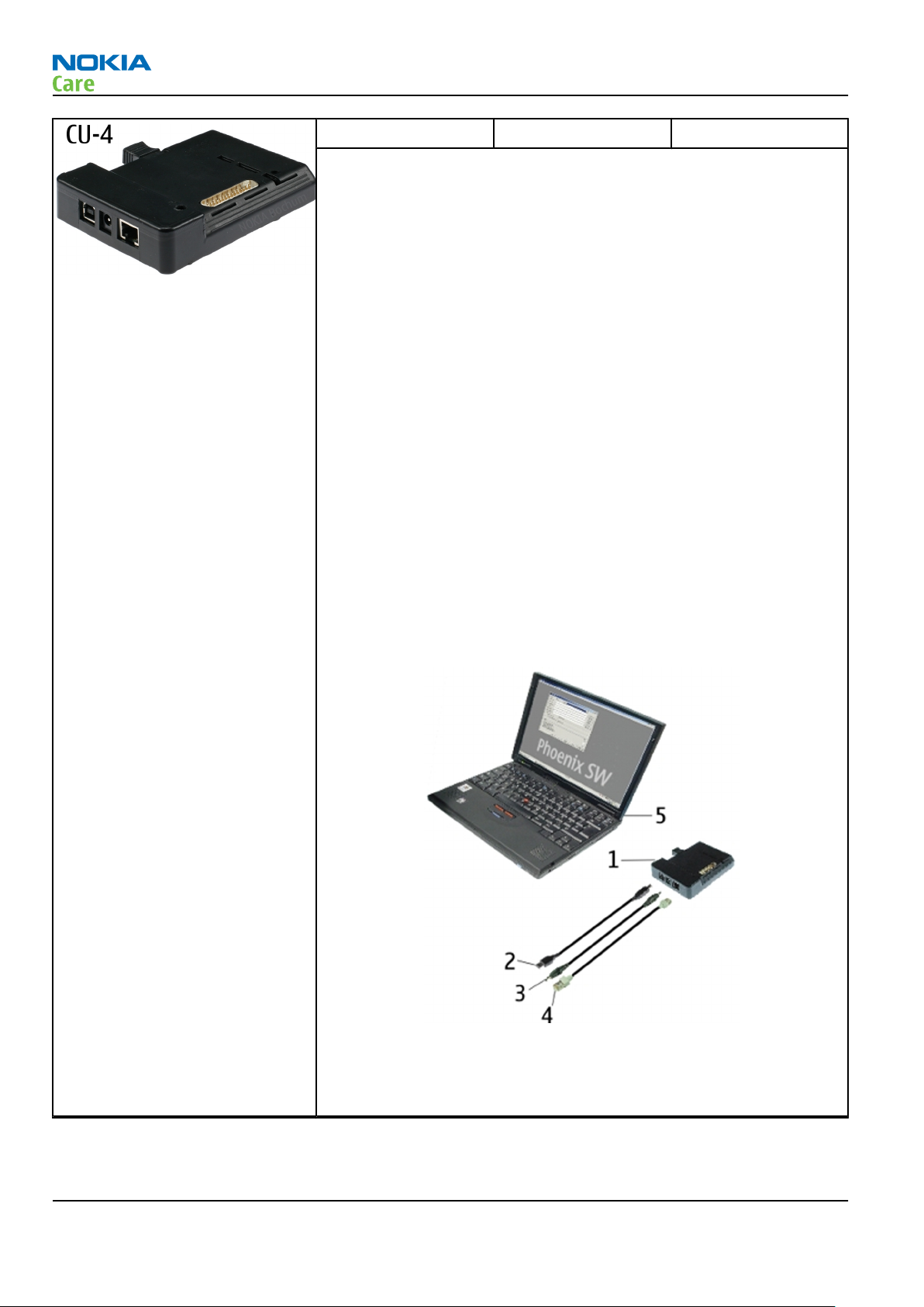
CU-4 Control unit CU-4 is a general service tool used with a module jig and/or a flash
adapter. It requires an external 12 V power supply.
The unit has the following features:
•
software controlled via USB
•
EM calibration function
•
Forwards FBUS/Flashbus traffic to/from terminal
•
Forwards USB traffic to/from terminal
•
software controlled BSI values
•
regulated VBATT voltage
•
2 x USB2.0 connector (Hub)
•
FBUS and USB connections supported
When using CU-4, note the special order of connecting cables and
other service equipment:
Instructions
1 Connect a service tool (jig, flash adapter) to CU-4.
2 Connect CU-4 to your PC with a USB cable.
3 Connect supply voltage (12 V)
4 Connect an FBUS cable (if necessary).
5 Start Phoenix service software.
Note: Phoenix enables CU-4 regulators via USB when it is
started.
Reconnecting the power supply requires a Phoenix restart.
Page 2 – 6 COMPANY CONFIDENTIAL Issue 1
Copyright © 2010 Nokia. All rights reserved.
Page 25
RM-497
Service Devices and Service Concepts
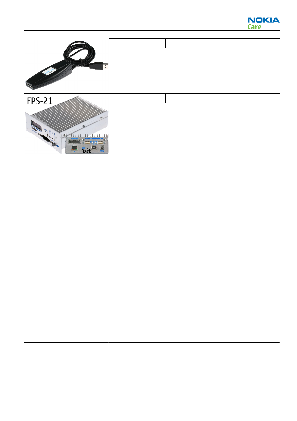
FLS-5 Flash device FLS-5 is a dongle and flash device incorporated into one package,
developed specifically for POS use.
Note: FLS-5 can be used as an alternative to PK-1.
FPS-21 Flash prommer
FPS-21 sales package:
•
FPS-21 prommer
•
AC-35 power supply
•
CA-31D USB cable
FPS-21 interfaces:
Front
•
Service cable connector
Provides Flashbus, USB and VBAT connections to a mobile device.
•
SmartCard socket
A SmartCard is needed to allow DCT-4 generation mobile device
programming.
Rear
•
DC power input
For connecting the external power supply (AC-35).
•
Two USB A type ports (USB1/USB3)
Can be used, for example, for connecting external storage memory
devices or mobile devices
•
One USB B type device connector (USB2)
For connecting a PC.
•
Phone connector
Service cable connection for connecting Flashbus/FLA.
•
Ethernet RJ45 type socket (LAN)
For connecting the FPS-21 to LAN.
Inside
•
Four SD card memory slots
For internal storage memory.
Note: In order to access the SD memory card slots inside
FPS-21, the prommer needs to be opened by removing the
front panel, rear panel and heatsink from the prommer body.
Issue 1 COMPANY CONFIDENTIAL Page 2 – 7
Copyright © 2010 Nokia. All rights reserved.
Page 26
RM-497
Service Devices and Service Concepts
PK-1 Software protection
key
PK-1 is a hardware protection key with a USB interface. It has the same
functionality as the PKD-1 series dongle.
PK-1 is meant for use with a PC that does not have a series interface.
To use this USB dongle for security service functions please register
the dongle in the same way as the PKD-1 series dongle.
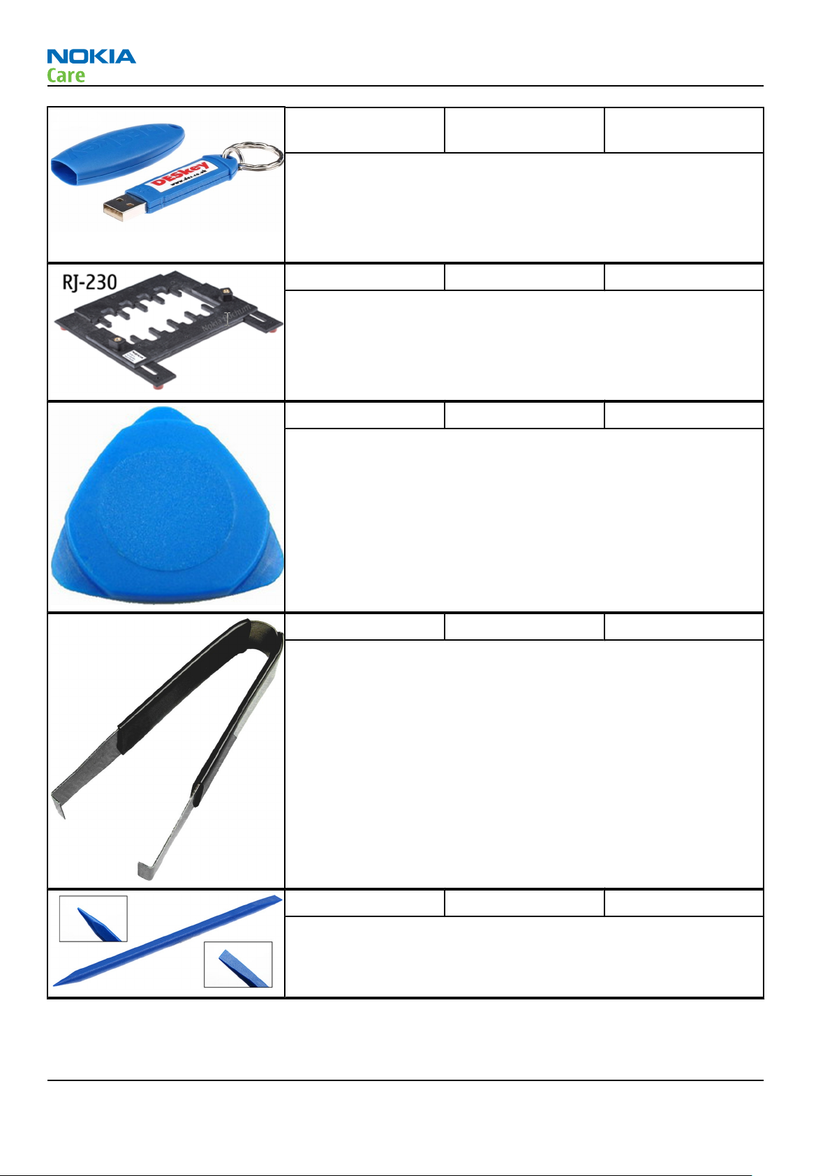
RJ-230 Common jig
RJ-230 is a jig used for soldering and as a rework jig for the engine
module.
SRT-6 Opening tool SRT-6 is used to open phone covers.
Note: The SRT-6 is included in the Nokia Standard Toolkit.
SS-34 Flex opening tool
SS-93 Blue stick tool SS-93 is used for general disassembly and assembly tasks.
Page 2 – 8 COMPANY CONFIDENTIAL Issue 1
Copyright © 2010 Nokia. All rights reserved.
Page 27
RM-497
Service Devices and Service Concepts
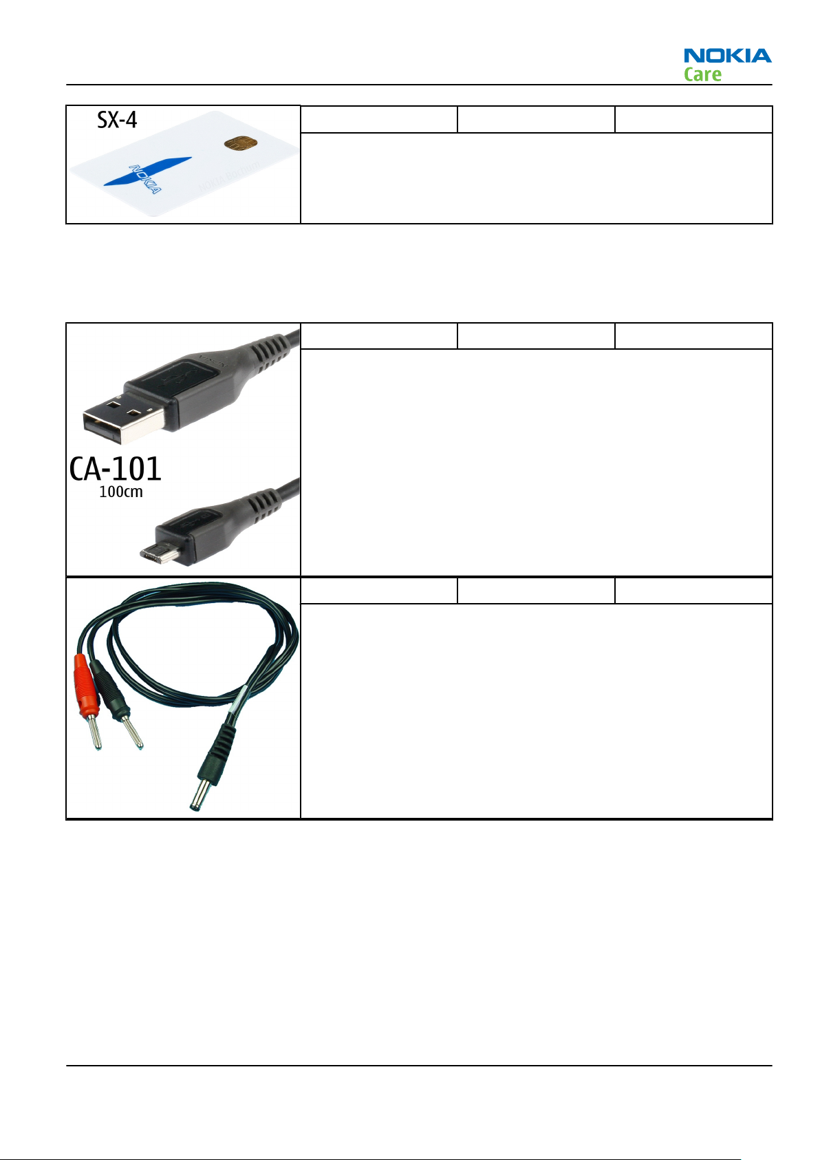
SX-4 Smart card SX-4 is a BB5 security device used to protect critical features in tuning
and testing.
SX-4 is also needed together with FPS-21 when DCT-4 phones are
flashed.
Cables
The table below gives a short overview of service devices that can be used for testing, error analysis, and
repair of product RM-497. For the correct use of the service devices, and the best effort of workbench setup,
please refer to various concepts.
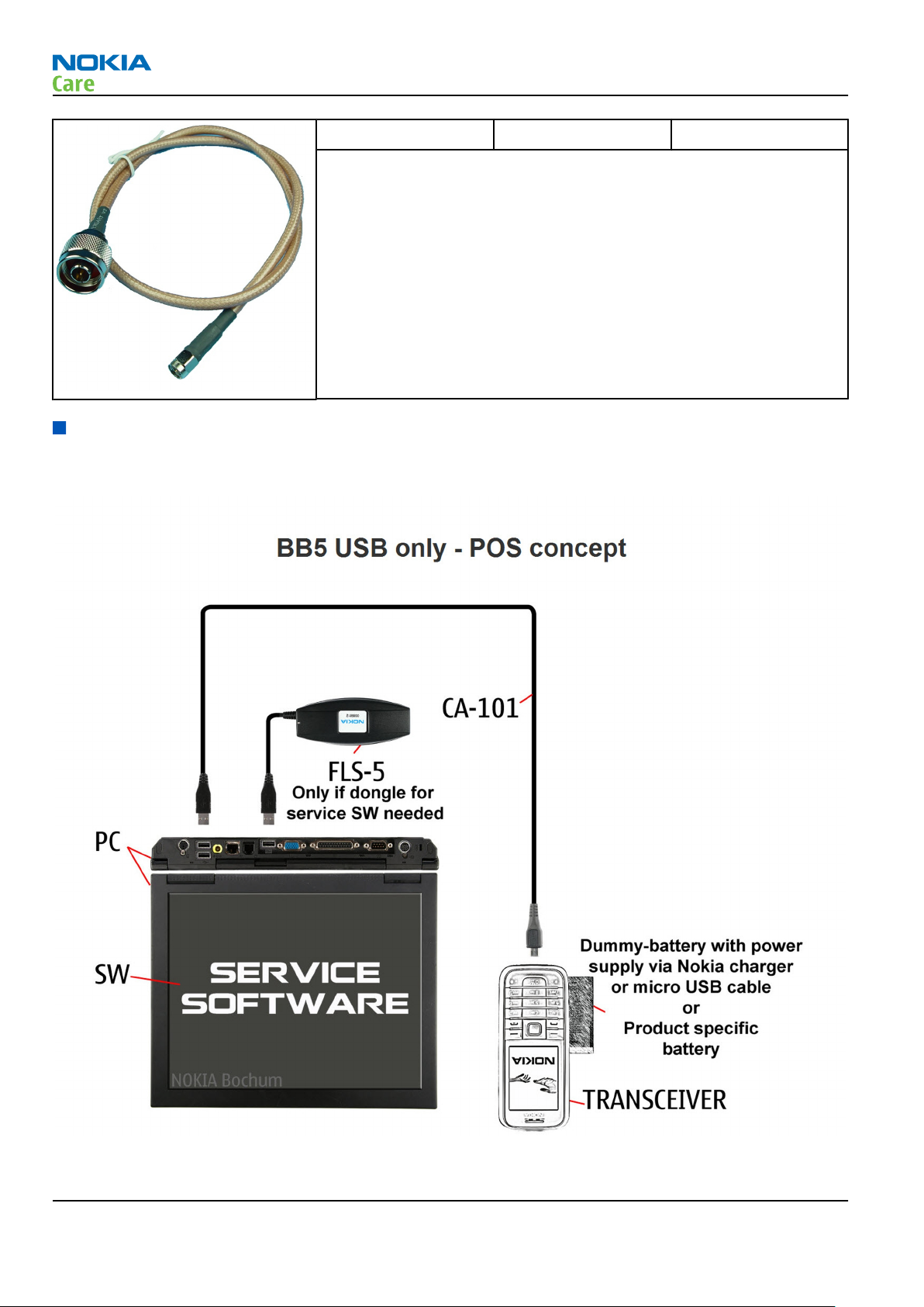
CA-101 Micro USB cable The CA-101 is a USB-to-microUSB data cable that allows connections
between the PC and the phone.
PCS-1 Power cable The PCS-1 power cable (DC) is used with a docking station, a module
jig or a control unit to supply a controlled voltage.
Issue 1 COMPANY CONFIDENTIAL Page 2 – 9
Copyright © 2010 Nokia. All rights reserved.
Page 28
Service concepts
POS (Point of Sale) flash concept
RM-497
Service Devices and Service Concepts
XRS-6 RF cable The RF cable is used to connect, for example, a module repair jig to
the RF measurement equipment.
SMA to N-Connector approximately 610 mm.
Attenuation for:
•
GSM850/900: 0.3+-0.1 dB
•
GSM1800/1900: 0.5+-0.1 dB
Figure 2 POS flash concept
Page 2 – 10 COMPANY CONFIDENTIAL Issue 1
Copyright © 2010 Nokia. All rights reserved.
Page 29
RM-497
Service Devices and Service Concepts
Basic flash concept L3
Figure 3 Basic flash concept L3
Issue 1 COMPANY CONFIDENTIAL Page 2 – 11
Copyright © 2010 Nokia. All rights reserved.
Page 30
Flash concept with FPS-21
RM-497
Service Devices and Service Concepts
Figure 4 Flash concept with FPS-21 (A)
Page 2 – 12 COMPANY CONFIDENTIAL Issue 1
Copyright © 2010 Nokia. All rights reserved.
Page 31

RM-497
Service Devices and Service Concepts
Figure 5 Flash concept with FPS-21 (B)
Issue 1 COMPANY CONFIDENTIAL Page 2 – 13
Copyright © 2010 Nokia. All rights reserved.
Page 32

Basic BB tune concept (EM calibration)
RM-497
Service Devices and Service Concepts
Figure 6 Basic BB tune concept (EM calibration)
Page 2 – 14 COMPANY CONFIDENTIAL Issue 1
Copyright © 2010 Nokia. All rights reserved.
Page 33

RM-497
Service Devices and Service Concepts
Basic RF&BB tune concept with FPS-21
Figure 7 Basic RF&BB tune concept with FPS-21 (A)
Issue 1 COMPANY CONFIDENTIAL Page 2 – 15
Copyright © 2010 Nokia. All rights reserved.
Page 34

RM-497
Service Devices and Service Concepts
Figure 8 Basic RF&BB tune concept with FPS-21 (B)
Page 2 – 16 COMPANY CONFIDENTIAL Issue 1
Copyright © 2010 Nokia. All rights reserved.
Page 35

Nokia Customer Care
3 — BB Troubleshooting and
Manual Tuning Guide
Issue 1 COMPANY CONFIDENTIAL Page 3 – 1
Copyright © 2010 Nokia. All rights reserved.
Page 36

RM-497
BB Troubleshooting and Manual Tuning Guide
(This page left intentionally blank.)
Page 3 – 2 COMPANY CONFIDENTIAL Issue 1
Copyright © 2010 Nokia. All rights reserved.
Page 37

RM-497
BB Troubleshooting and Manual Tuning Guide
Table of Contents
Introduction to BB Troubleshooting ................................................................................................................... 3–5
Baseband self tests in Phoenix ............................................................................................................................ 3–5
Power and charging troubleshooting................................................................................................................. 3–7
Dead or jammed device troubleshooting...................................................................................................... 3–7
General power checking.................................................................................................................................. 3–8
Charging troubleshooting ............................................................................................................................ 3–11
Clocking troubleshooting ............................................................................................................................. 3–13
Power On key troubleshooting.................................................................................................................... 3–17
Interface troubleshooting ................................................................................................................................. 3–19
Flash Programming Troubleshooting ......................................................................................................... 3–19
Memory Troubleshooting............................................................................................................................. 3–21
Memory Card Troubleshooting .................................................................................................................... 3–23
SIM Card Troubleshooting ............................................................................................................................ 3–24
USB Interface Troubleshooting.................................................................................................................... 3–27
User interface troubleshooting......................................................................................................................... 3–29
Backlight and Illumination Troubleshooting ............................................................................................. 3–29
Display Interface Troubleshooting .............................................................................................................. 3–32
Camera troubleshooting.................................................................................................................................... 3–34
Camera HW Troubleshooting ....................................................................................................................... 3–34
Bad Camera Image Quality Troubleshooting ............................................................................................. 3–34
Audio troubleshooting....................................................................................................................................... 3–36
Audio troubleshooting test instructions..................................................................................................... 3–36
Internal microphone troubleshooting........................................................................................................ 3–39
Internal Handsfree (IHF) Speaker Troubleshooting................................................................................... 3–42
External earpiece troubleshooting.............................................................................................................. 3–44
External microphone troubleshooting........................................................................................................ 3–46
Accelerometer Sensor Troubleshooting........................................................................................................... 3–47
Accelerometer Troubleshooting .................................................................................................................. 3–47
Baseband manual tuning guide........................................................................................................................ 3–49
Certificate restoring ...................................................................................................................................... 3–49
Energy management calibration................................................................................................................. 3–50
List of Tables
Table 1 Calibration value limits ........................................................................................................................ 3–51
List of Figures
Figure 9 Troubleshooting Component Location ............................................................................................. 3–16
Figure 10 Probe placement ............................................................................................................................... 3–20
Figure 11 Probe placement diagram................................................................................................................ 3–22
Figure 12 Probe placement diagram................................................................................................................ 3–24
Figure 13 Probe placement diagram................................................................................................................ 3–25
Figure 14 Probe placement diagram................................................................................................................ 3–28
Figure 15 Probe placement diagram................................................................................................................ 3–31
Figure 16 Probe placement diagram................................................................................................................ 3–33
Figure 17 Internal microphone troubleshooting probe placement diagram .............................................. 3–40
Figure 18 IHF troubleshooting probe placement diagram ............................................................................ 3–43
Figure 19 External earpiece troubleshooting probe placement diagram.................................................... 3–44
Figure 20 External microphone troubleshooting placement diagram......................................................... 3–46
Issue 1 COMPANY CONFIDENTIAL Page 3 – 3
Copyright © 2010 Nokia. All rights reserved.
Page 38

RM-497
BB Troubleshooting and Manual Tuning Guide
Figure 21 Accelerometer troubleshooting probe placement diagram......................................................... 3–49
Page 3 – 4 COMPANY CONFIDENTIAL Issue 1
Copyright © 2010 Nokia. All rights reserved.
Page 39

RM-497
BB Troubleshooting and Manual Tuning Guide
Introduction to BB Troubleshooting
Nearly all of the functions of the phone are contained within or controlled by the D2800 Juno BB ASIC so most
of the debugging will be centered there. The D2800 Juno BB ASIC is static sensitive so precautions must be
taken to avoid damaging this or other devices from excessive ESD.
Baseband self tests in Phoenix
Context
Always start the trouble-shooting procedure by running the Phoenix self tests. If a test fails, please follow
the diagram in the
If the phone is dead and you cannot perform the self-test, please go to
Troubleshooting.
Note: The phone must be powered-down and in the PWR_OFF state when replacing components.
Baseband Main Troubleshooting
section.
Dead or Jammed Device
Issue 1 COMPANY CONFIDENTIAL Page 3 – 5
Copyright © 2010 Nokia. All rights reserved.
Page 40

Troubleshooting flow
RM-497
BB Troubleshooting and Manual Tuning Guide
Page 3 – 6 COMPANY CONFIDENTIAL Issue 1
Copyright © 2010 Nokia. All rights reserved.
Page 41

RM-497
BB Troubleshooting and Manual Tuning Guide
Power and charging troubleshooting
Dead or jammed device troubleshooting
Troubleshooting flow
Issue 1 COMPANY CONFIDENTIAL Page 3 – 7
Copyright © 2010 Nokia. All rights reserved.
Page 42

Troubleshooting flow
RM-497
BB Troubleshooting and Manual Tuning Guide
Page 3 – 8 COMPANY CONFIDENTIAL Issue 1
Copyright © 2010 Nokia. All rights reserved.
Page 43

RM-497
BB Troubleshooting and Manual Tuning Guide
General power checking
Check the following supply voltages from the N2201 Loviisa PMU to the D2800 Juno BB ASIC:
Signal name Regulator Sleep Active Main user Probe point Nominal
voltage (V)
VUSB2 VMSLDO2 ON ON NVM digital
supply, analog
supply for USB
I/O
VIO VIOLDO ON ON CMOS I/O
digital supply,
digital supply
for BBL I/O
VCORE VCSRL ON ON core digital
supply, digital
supply for RF,
analog supply
for USB PLL
VRF2 VRFLDO1 OFF ON analog supply
for RF
VRF1 VLVLDO2 OFF ON analog supply
for RF
VDCXO VLCLDO OFF ON analog supply
for RF
VSIM VSIMLDO TBD ON digital supply
for SIM I/O
C2219 3.3
C2222 1.8
C2200 1.2/1.01
C2214 2.7
C2209 1.3
C2212 1.3
C2215 3.0
VAMP2 VHCLDO2 OFF ON digital supply
for SDIO I/O
VMEM VIOSRL ON ON digital supply
for nvSRAM I/
O, digital
supply for EMI
I/O
VANA1 VLVLDO1 ON ON analog supply
for MainPLL,
analog supply
for AppsPLL,
analog supply
for USB,
analog supply
for USB, CSI-2/
CCP2 I/O, DSI I/
O, analog
supply for dual
DAC
C2216 1.8
C2201 1.8
C2208 1.2
Issue 1 COMPANY CONFIDENTIAL Page 3 – 9
Copyright © 2010 Nokia. All rights reserved.
Page 44

RM-497
BB Troubleshooting and Manual Tuning Guide
Signal name Regulator Sleep Active Main user Probe point Nominal
voltage (V)
VOUT VRFLDO2 ON ON analog supply
for USB and ACI
VANA2 VALDO2 ON ON analog supply
for ADC (4to-1) and IHF
VANA3 VALDO1 ON ON analog supply
for
microphone
and Aux ADC/
DAC,
VAMP1 VHCLDO1 OFF ON analog supply
for DDAC left
outputs,
analog supply
for DDAC right
and left
outputs, Vibra
VCORE will be trimmed to approximately 1.0V in the Sleep mode.
C2213 2.5
C2211 2.5
C2210 3.0
C2207, C2217 3.0
Page 3 – 10 COMPANY CONFIDENTIAL Issue 1
Copyright © 2010 Nokia. All rights reserved.
Page 45

RM-497
BB Troubleshooting and Manual Tuning Guide
Issue 1 COMPANY CONFIDENTIAL Page 3 – 11
Copyright © 2010 Nokia. All rights reserved.
Page 46

Charging troubleshooting
Wall Charger Troubleshooting
RM-497
BB Troubleshooting and Manual Tuning Guide
Page 3 – 12 COMPANY CONFIDENTIAL Issue 1
Copyright © 2010 Nokia. All rights reserved.
Page 47

RM-497
BB Troubleshooting and Manual Tuning Guide
Component Placement
Clocking troubleshooting
Context
The D2800 Juno BB ASIC requires two clocks for proper operation. Both are provided by on-board crystals.
Issue 1 COMPANY CONFIDENTIAL Page 3 – 13
Copyright © 2010 Nokia. All rights reserved.
Page 48

RM-497
BB Troubleshooting and Manual Tuning Guide
•
The 32 kHz crystal is connected to the N2201 PMU and is transmitted to the D2800 Juno BB ASIC.
•
The 26 MHz crystal is connected directly to the D2800 Juno BB ASIC. The D2800 Juno BB ASIC can output
four copies of the 26 MHz input clock from it’s CK1, CK2, RF_XON, and RF_XOP pins, however, only the RF_XON
output is used.
Note: All test-points are located under the RF shielding.
1) 32 kHz crystal (B2200)
The 32 kHz clock to the N2201 Loviisa can be tested by setting the oscilloscope probe on R2209.
2) 26 MHz crystal (B2800)
•
The 26 MHz clock to the D2800 Juno can be tested by setting the oscilloscope probe on B2800.
•
The RF_XON output clock can be tested by probing C6094 near the BT/FM module.
Note: This step will require the RF_XON output clock for BT/FM module to be enabled through
Phoenix SW.
Page 3 – 14 COMPANY CONFIDENTIAL Issue 1
Copyright © 2010 Nokia. All rights reserved.
Page 49

RM-497
BB Troubleshooting and Manual Tuning Guide
Troubleshooting flow
Issue 1 COMPANY CONFIDENTIAL Page 3 – 15
Copyright © 2010 Nokia. All rights reserved.
Page 50

Troubleshooting flow
RM-497
BB Troubleshooting and Manual Tuning Guide
Figure 9 Troubleshooting Component Location
Page 3 – 16 COMPANY CONFIDENTIAL Issue 1
Copyright © 2010 Nokia. All rights reserved.
Page 51

RM-497
BB Troubleshooting and Manual Tuning Guide
Power On key troubleshooting
Troubleshooting flow
Issue 1 COMPANY CONFIDENTIAL Page 3 – 17
Copyright © 2010 Nokia. All rights reserved.
Page 52

RM-497
BB Troubleshooting and Manual Tuning Guide
Page 3 – 18 COMPANY CONFIDENTIAL Issue 1
Copyright © 2010 Nokia. All rights reserved.
Page 53

RM-497
BB Troubleshooting and Manual Tuning Guide
Interface troubleshooting
Flash Programming Troubleshooting
Troubleshooting flow
Issue 1 COMPANY CONFIDENTIAL Page 3 – 19
Copyright © 2010 Nokia. All rights reserved.
Page 54

RM-497
BB Troubleshooting and Manual Tuning Guide
Figure 10 Probe placement
Page 3 – 20 COMPANY CONFIDENTIAL Issue 1
Copyright © 2010 Nokia. All rights reserved.
Page 55

RM-497
BB Troubleshooting and Manual Tuning Guide
Memory Troubleshooting
Troubleshooting flow
Issue 1 COMPANY CONFIDENTIAL Page 3 – 21
Copyright © 2010 Nokia. All rights reserved.
Page 56

RM-497
BB Troubleshooting and Manual Tuning Guide
Figure 11 Probe placement diagram
Page 3 – 22 COMPANY CONFIDENTIAL Issue 1
Copyright © 2010 Nokia. All rights reserved.
Page 57

RM-497
BB Troubleshooting and Manual Tuning Guide
Memory Card Troubleshooting
Troubleshooting flow
Issue 1 COMPANY CONFIDENTIAL Page 3 – 23
Copyright © 2010 Nokia. All rights reserved.
Page 58

RM-497
BB Troubleshooting and Manual Tuning Guide
Figure 12 Probe placement diagram
SIM Card Troubleshooting
Context
Note:
Battery must be inserted in order to power-up the phone, which will block access to the SIM and surrounding
components for probing.
Page 3 – 24 COMPANY CONFIDENTIAL Issue 1
Copyright © 2010 Nokia. All rights reserved.
Page 59

RM-497
BB Troubleshooting and Manual Tuning Guide
Troubleshooting flow
Issue 1 COMPANY CONFIDENTIAL Page 3 – 25
Copyright © 2010 Nokia. All rights reserved.
Page 60

RM-497
BB Troubleshooting and Manual Tuning Guide
Figure 13 Probe placement diagram
Page 3 – 26 COMPANY CONFIDENTIAL Issue 1
Copyright © 2010 Nokia. All rights reserved.
Page 61

RM-497
BB Troubleshooting and Manual Tuning Guide
USB Interface Troubleshooting
Troubleshooting flow
Issue 1 COMPANY CONFIDENTIAL Page 3 – 27
Copyright © 2010 Nokia. All rights reserved.
Page 62

RM-497
BB Troubleshooting and Manual Tuning Guide
Figure 14 Probe placement diagram
Page 3 – 28 COMPANY CONFIDENTIAL Issue 1
Copyright © 2010 Nokia. All rights reserved.
Page 63

RM-497
BB Troubleshooting and Manual Tuning Guide
User interface troubleshooting
Backlight and Illumination Troubleshooting
Troubleshooting flow
Issue 1 COMPANY CONFIDENTIAL Page 3 – 29
Copyright © 2010 Nokia. All rights reserved.
Page 64

RM-497
BB Troubleshooting and Manual Tuning Guide
Page 3 – 30 COMPANY CONFIDENTIAL Issue 1
Copyright © 2010 Nokia. All rights reserved.
Page 65

RM-497
BB Troubleshooting and Manual Tuning Guide
Figure 15 Probe placement diagram
Issue 1 COMPANY CONFIDENTIAL Page 3 – 31
Copyright © 2010 Nokia. All rights reserved.
Page 66

Display Interface Troubleshooting
Troubleshooting flow
RM-497
BB Troubleshooting and Manual Tuning Guide
Page 3 – 32 COMPANY CONFIDENTIAL Issue 1
Copyright © 2010 Nokia. All rights reserved.
Page 67

RM-497
BB Troubleshooting and Manual Tuning Guide
Figure 16 Probe placement diagram
Issue 1 COMPANY CONFIDENTIAL Page 3 – 33
Copyright © 2010 Nokia. All rights reserved.
Page 68

Camera troubleshooting
Camera HW Troubleshooting
Troubleshooting flow
RM-497
BB Troubleshooting and Manual Tuning Guide
Page 3 – 34 COMPANY CONFIDENTIAL Issue 1
Copyright © 2010 Nokia. All rights reserved.
Page 69

RM-497
BB Troubleshooting and Manual Tuning Guide
Bad Camera Image Quality Troubleshooting
Troubleshooting flow
Issue 1 COMPANY CONFIDENTIAL Page 3 – 35
Copyright © 2010 Nokia. All rights reserved.
Page 70

RM-497
BB Troubleshooting and Manual Tuning Guide
Audio troubleshooting
Audio troubleshooting test instructions
Differential external earpiece and internal earpiece outputs can be measured either with a single-ended or
a differential probe.
When measuring with a single-ended probe, each output is measured against the ground.
Internal handsfree output is measured using a current probe, if a special low-pass filter designed for
measuring a digital amplifier is not available. Note also that when using a current probe, the input signal
frequency must be set to 1kHz.
The input signal for each loop test can be either single-ended or differential.
Required equipment
The following equipments are needed for the tests:
•
Oscilloscope
•
Function generator (sine waveform)
•
'Active speaker' or 'speaker and power amplifier'
•
Sound level meter
•
Current probe (Internal handsfree DPMA output measurement)
•
Phoenix service software
•
Battery voltage 3.7V
Test procedure
Audio can be tested using the Phoenix audio routings option. Three different audio loop paths can be
activated:
•
External microphone to internal earpiece
•
External microphone to internal handsfree speaker
•
Internal microphone to external earpiece
Each audio loop sets routing from the specified input to the specified output enabling a quick in-out test.
Loop path gains are fixed and they cannot be changed using Phoenix. Correct pins and signal for each test
are presented in the following table.
Phoenix audio loop tests and test results
The results presented in the table apply when no accessory is connected and battery voltage is set to 3.7V.
Earpiece, internal microphone and speaker are in place during measurement. Applying a headset accessory
during measurement causes a significant drop in measured quantities.
The gain values presented in the table apply for a different output vs. single-ended/different input.
Page 3 – 36 COMPANY CONFIDENTIAL Issue 1
Copyright © 2010 Nokia. All rights reserved.
Page 71

RM-497
BB Troubleshooting and Manual Tuning Guide
Loop
test
Exter
nal
Mic to
Exter
nal
Earpi
ece
Exter
nal
Mic to
Inter
nal
Earpi
ece
Input
termin
al
MIC2P
(C2829
) and
GND
MIC2N
(C2830
) and
GND
MIC2P
(C2829
) and
GND
MIC2N
(C2830
) and
GND
Output
terminal
HS_EAR_L
[E3485] and
GND
HS_EAR_R
[E3484] and
GND
HS_EAR_L
[E3485] and
GND
HS_EAR_R
[E3484] and
GND
EARP [R2106]
not assembled
and GND
EARN [R2107]
not assembled
and GND
EARP [R2106]
not assembled
and GND
EARN [R2107]
not assembled
and GND
Mic Tx
PGA gain
[dB]
0 -3 1000 710 1.2 NA
0 -3 1000 710 1.2 NA
Rx PGA
gain
Input
voltage
[mVp-p]
Differential
output
voltage
[mVp-p]
Output
DC level
[V]
current
Output
[mA]
Exter
nal
Mic to
Inter
nal
hand
sfree
Issue 1 COMPANY CONFIDENTIAL Page 3 – 37
MIC2P
(C2829
) and
GND
MIC2N
(C2830
) and
GND
HFSPP [E3420] 0 -3 1000 710 0 25mA
HFSPN [E3421]
HFSPP [E3420]
HFSPN [E3421]
Copyright © 2010 Nokia. All rights reserved.
(calc.)
Page 72

RM-497
BB Troubleshooting and Manual Tuning Guide
Loop
test
Inter
nal
Mic to
Exter
nal
Earpi
ece
Input
termin
al
MIC1P
(C2107
)
MIC1N
(C2108
)
Output
terminal
HS_EAR_L
[E3485] and
GND
HS_EAR_R
[E3484] and
GND
HS_EAR_L
[E3485] and
GND
HS_EAR_R
[E3484] and
GND
Mic Tx
PGA gain
[dB]
0 -3 1000 710 1.2 NA
Rx PGA
gain
Input
voltage
[mVp-p]
Differential
output
voltage
[mVp-p]
Output
DC level
[V]
current
Output
[mA]
Page 3 – 38 COMPANY CONFIDENTIAL Issue 1
Copyright © 2010 Nokia. All rights reserved.
Page 73

RM-497
BB Troubleshooting and Manual Tuning Guide
Placement Diagram
Issue 1 COMPANY CONFIDENTIAL Page 3 – 39
Copyright © 2010 Nokia. All rights reserved.
Page 74

Internal microphone troubleshooting
Troubleshooting flow
RM-497
BB Troubleshooting and Manual Tuning Guide
Page 3 – 40 COMPANY CONFIDENTIAL Issue 1
Copyright © 2010 Nokia. All rights reserved.
Page 75

RM-497
BB Troubleshooting and Manual Tuning Guide
Figure 17 Internal microphone troubleshooting probe placement diagram
Issue 1 COMPANY CONFIDENTIAL Page 3 – 41
Copyright © 2010 Nokia. All rights reserved.
Page 76

Internal Handsfree (IHF) Speaker Troubleshooting
Troubleshooting flow
RM-497
BB Troubleshooting and Manual Tuning Guide
Page 3 – 42 COMPANY CONFIDENTIAL Issue 1
Copyright © 2010 Nokia. All rights reserved.
Page 77

RM-497
BB Troubleshooting and Manual Tuning Guide
Figure 18 IHF troubleshooting probe placement diagram
Issue 1 COMPANY CONFIDENTIAL Page 3 – 43
Copyright © 2010 Nokia. All rights reserved.
Page 78

External earpiece troubleshooting
Troubleshooting flow
RM-497
BB Troubleshooting and Manual Tuning Guide
Page 3 – 44 COMPANY CONFIDENTIAL Issue 1
Copyright © 2010 Nokia. All rights reserved.
Page 79

RM-497
BB Troubleshooting and Manual Tuning Guide
Figure 19 External earpiece troubleshooting probe placement diagram
Issue 1 COMPANY CONFIDENTIAL Page 3 – 45
Copyright © 2010 Nokia. All rights reserved.
Page 80

External microphone troubleshooting
Troubleshooting flow
RM-497
BB Troubleshooting and Manual Tuning Guide
Page 3 – 46 COMPANY CONFIDENTIAL Issue 1
Copyright © 2010 Nokia. All rights reserved.
Page 81

RM-497
BB Troubleshooting and Manual Tuning Guide
Figure 20 External microphone troubleshooting placement diagram
Accelerometer Sensor Troubleshooting
Accelerometer Troubleshooting
Context
Accelerometer self-test:
(ST_ACCELEROMETER_TEST) verifies the digital parts and the sensor elements inside the component. Self-test
is available in LOCAL and TEST modes.
Issue 1 COMPANY CONFIDENTIAL Page 3 – 47
Copyright © 2010 Nokia. All rights reserved.
Page 82

Note: The device needs to be stable when running the self-test to get correct results. If changes in
acceleration are detected by the component during the test, it may cause the self-test to fail.
Troubleshooting flow
RM-497
BB Troubleshooting and Manual Tuning Guide
Page 3 – 48 COMPANY CONFIDENTIAL Issue 1
Copyright © 2010 Nokia. All rights reserved.
Page 83

RM-497
BB Troubleshooting and Manual Tuning Guide
Figure 21 Accelerometer troubleshooting probe placement diagram
Baseband manual tuning guide
Certificate restoring
Context
This procedure is performed when the device certificate is corrupted for some reason.
All tunings (RF & Baseband, UI) must be done after performing the certificate restoring procedure.
The procedure for certificate restoring is the following:
•
Flash the phone with the latest available software using FPS-10 and FPS-21.
Note: If the COMBO memory of a phone is replaced, the ENO SW must be flashed first before
performing the "normal" firmware flashing.
•
Execute the certificate restore process in Phoenix.
Issue 1 COMPANY CONFIDENTIAL Page 3 – 49
Copyright © 2010 Nokia. All rights reserved.
Page 84

BB Troubleshooting and Manual Tuning Guide
•
Tune the phone completely.
Note: SX-4 smart card is needed.
•
If the phone resets after certificate restoring, reflash the phone again.
Required equipment and setup:
•
Phoenix
•
The latest phone model specific
•
PK-1 dongle
•
SX-4 smart card (Enables testing and tuning features)
•
Activated FPS-10 OR FPS-21 flash prommer OR External smart card reader
•
Latest flash update package for FPS-10 or FPS-21 flash prommers
•
CU-4 control unit
•
USB cable from PC USB Port to CU-4 control unit
•
PCS-1 cable to power CU-4 from external power supply
•
XCS-4 modular cable between flash prommer and CU-4
service software supporting RM-586.
Phoenix
Note: CU-4 must be supplied with +12 V from an external power supply in all steps of certificate
restoring.
data package.
RM-497
Steps
1. Program the phone software.
Note: If the COMBO memory of a phone is replaced, the ENO SW must be flashed first before
performing the "normal" firmware flashing.
2. Execute the certificate restore process in
Phoenix
.
Next actions
After a successful rewrite, you must retune the phone completely by using
Important: Perform all tunings: RF, BB, and UI.
Energy management calibration
Phoenix
tuning functions.
Prerequisites
Energy Management (EM) calibration is performed to calibrate the setting (gain and offset) of AD converters
in several channels (that is, battery voltage, BSI, battery current) to get an accurate AD conversion result.
Hardware setup:
•
An external power supply is needed.
•
Supply 12V DC from an external power supply to CU-4 to power up the phone.
•
The phone must be connected to a CU-4 control unit with a product-specific flash adapter.
Steps
1. Connect CU-4 with MJ-249, and place phone to the Module jig MJ-249.
2. Start
3. Choose File → Scan Product.
4. Choose Tuning → Energy Management Calibration.
5. To show the current values in the phone memory, click Read, and check that communication between
Page 3 – 50 COMPANY CONFIDENTIAL Issue 1
Phoenix
the phone and CU-4 works.
service software.
Copyright © 2010 Nokia. All rights reserved.
Page 85

RM-497
BB Troubleshooting and Manual Tuning Guide
6. Check that the CU-4 used check box is checked.
7. Select the item(s) to be calibrated.
Note: ADC calibration has to be performed before other item(s). However, if all calibrations are
selected at the same time, there is no need to perform the ADC calibration first.
8. Click Tune.
9. The calibration of the selected item(s) is carried out automatically.
Note: Phoenix_Service_Software_2010_8_3_41402 or afterward version can support Automatic
tuning.
10. Click Calculate.
11. The candidates for the new calibration values are shown in the Calculated Values column. If the new
calibration values seem to be acceptable (please refer to the following "Calibration value limits" table),
click Write to store the new calibration values to the phone permanent memory.
Table 1 Calibration value limits
Parameter Min. Max.
ADC Offset - -3
ADC Gain - 13183
BSI Gain - 1174
VBAT Offset - 2515
VBAT Gain - 21450
IBAT (ICal) Gain - 10001
12. Click Read, and confirm that the new calibration values are stored in the phone memory correctly. If the
values are not stored to the phone memory, click Write and/or repeat the procedure again.
13. end the procedure, close the
Energy Management Calibration
window.
Issue 1 COMPANY CONFIDENTIAL Page 3 – 51
Copyright © 2010 Nokia. All rights reserved.
Page 86

RM-497
BB Troubleshooting and Manual Tuning Guide
(This page left intentionally blank.)
Page 3 – 52 COMPANY CONFIDENTIAL Issue 1
Copyright © 2010 Nokia. All rights reserved.
Page 87

Nokia Customer Care
4 — RF troubleshooting
Issue 1 COMPANY CONFIDENTIAL Page 4 – 1
Copyright © 2010 Nokia. All rights reserved.
Page 88

RM-497
RF troubleshooting
(This page left intentionally blank.)
Page 4 – 2 COMPANY CONFIDENTIAL Issue 1
Copyright © 2010 Nokia. All rights reserved.
Page 89

RM-497
RF troubleshooting
Table of Contents
General RF troubleshooting ................................................................................................................................. 4–5
Introduction to RF troubleshooting ............................................................................................................... 4–5
RF key components .......................................................................................................................................... 4–6
Auto tuning for RF ................................................................................................................................................. 4–6
General RF voltage checking ................................................................................................................................ 4–7
General voltage checking ................................................................................................................................ 4–7
FEM Control Signal............................................................................................................................................ 4–8
Receiver troubleshooting .................................................................................................................................. 4–12
Introduction to receiver (RX) troubleshooting........................................................................................... 4–12
RF Test Points in RX Troubleshooting ......................................................................................................... 4–13
GSM RX chain activation for manual measurements/GSM RSSI measurement ....................................... 4–13
RX troubleshooting for GSM850................................................................................................................... 4–15
RX troubleshooting for GSM900................................................................................................................... 4–15
RX troubleshooting for GSM1800................................................................................................................. 4–17
RX troubleshooting for GSM1900................................................................................................................. 4–17
Transmitter troubleshooting ............................................................................................................................ 4–18
Introduction to transmitter (TX) troubleshooting..................................................................................... 4–18
RF Test Points in TX Troubleshooting.......................................................................................................... 4–19
RF Transmitter Self-test ................................................................................................................................ 4–19
TX troubleshooting for GSM850/900........................................................................................................... 4–23
TX troubleshooting for DCS1800/PCS1800.................................................................................................. 4–23
GSM transmitter troubleshooting................................................................................................................ 4–24
List of Tables
Table 2 21351/Juno Supplies ............................................................................................................................... 4–7
Table 3 FEM Supplies/Control Signals.................................................................................................................. 4–8
Table 4 FEM Control Logics ................................................................................................................................... 4–8
Table 5 Signals Coverage in RFPA Self-test Option.......................................................................................... 4–19
List of Figures
Figure 22 RF key components .............................................................................................................................. 4–6
Figure 23 Auto tuning concept with CMU200..................................................................................................... 4–7
Figure 24 General voltage checking test points (main board, bottom side) .................................................. 4–8
Figure 25 GMSK Control Signal in time domain............................................................................................... 4–12
Figure 26 RF transmitter & receiver test points .............................................................................................. 4–13
Figure 27 RF transmitter & receiver test points .............................................................................................. 4–19
Figure 28 Analyzer setting................................................................................................................................. 4–25
Figure 29 Phase error......................................................................................................................................... 4–26
Figure 30 Modulation/Switching spectrum ..................................................................................................... 4–26
Figure 31 Power/Burst....................................................................................................................................... 4–27
Figure 32 Edge.................................................................................................................................................... 4–27
Issue 1 COMPANY CONFIDENTIAL Page 4 – 3
Copyright © 2010 Nokia. All rights reserved.
Page 90

RM-497
RF troubleshooting
(This page left intentionally blank.)
Page 4 – 4 COMPANY CONFIDENTIAL Issue 1
Copyright © 2010 Nokia. All rights reserved.
Page 91

RM-497
RF troubleshooting
General RF troubleshooting
Introduction to RF troubleshooting
Most RF semiconductors are static discharge sensitive
ESD protection must be applied during repair (ground straps and ESD soldering irons).
Pre-baking
These parts are moisture sensitive and must be pre-baked prior to soldering:
•
Juno D2800
•
Front End Module N7500
Discrete components
In addition to the key-components, there are a number of discrete components (resistors, inductors, and
capacitors) for which troubleshooting is done mainly by
Capacitors: check for short circuits.
Resistors: check value with an ohm meter.
Inductors: check for open circuits.
Note: In-circuit measurements should be evaluated carefully.
visual inspection
.
Measuring equipment
All measurements should be done using:
•
An oscilloscope for low frequency and DC measurements. Recommended probe: 10:1, 10Mohm//8pF.
•
A radio communication tester including RF generator and spectrum analyser, for example Rohde & Schwarz
CMU200. (Alternatively a spectrum analyser and an RF generator can be used. Some tests in this guide are
not possible to perform if this solution is chosen).
Note: All measurements with an RF coupler should be performed in an RF-shielded environment
because nearby base stations can disturb sensitive receiver measurements. If there is no possibility
to use RF shielded environment, testing at frequencies of nearby base stations should be avoided.
Level of repair
The scope of this guideline is to enable repairs at key-component level. Some key-components are not
accessible, i.e. not replaceable. Please refer to the list of Non-replaceable RF components.
Note: After the RF shielding can is removed (for measurement or repair), it must be replaced with
a new one and cannot be reused.
Issue 1 COMPANY CONFIDENTIAL Page 4 – 5
Copyright © 2010 Nokia. All rights reserved.
Page 92

RF key components
RM-497
RF troubleshooting
Figure 22 RF key components
Auto tuning for RF
This phone can be tuned automatically.
Autotune is designed to align the phone's RF part easier and faster. It performs calibrations, tunings and
measurements of RX and TX. The results are displayed and logged in a result file, if initiated.
Hardware set up
Hardware requirements for auto tuning:
•
PC (Windows 2000/XP) with GPIB card
•
Power supply
•
Product specific module jig
•
Cables: XRF-1 (RF cable), USB cable, GBIP cable and DAU-9S
•
Signal analyser (TX), signal generator (RX) and RF-splitter or one device including all.
Page 4 – 6 COMPANY CONFIDENTIAL Issue 1
Copyright © 2010 Nokia. All rights reserved.
Page 93

RM-497
RF troubleshooting
Figure 23 Auto tuning concept with CMU200
Note: Crossover Cable connection between computer and CMU200 is recommended (refer to Service
devices chapter and Module Jig concepts).
Phoenix and config file preparations
Install the phone specific data package. This defines phone specific settings.
Setup a new folder under
Phoenix -> Products
, rename it as RM-586, copy voyager_rf.xml to this folder.
Auto tuning procedure
1 Make sure the phone (in the jig) is connected to the equipment. Else, some menus will not be shown in
Phoenix.
2 To go to autotune, select
3 Start autotuning, clicking the
Tuning (Alt-U)
Tune
button.
>
Auto-Tune (Alt-A)
from the menu.
General RF voltage checking
General voltage checking
Steps
1. Set up the engine board in the module jig. The phone should be in local mode.
2. Check the following:
Table 2 21351/Juno Supplies
# Signal Name Test Point Voltage (All Bands)
1 VDCXO (INT_VDCXO) C2813 1.3V (analog supply for DCXO)
2 VRF1 (VRF1_RX, VRF1_PLL, VRF1_TXPLL) C2817 or
C2819 or
C2868
1.3V (analog supply for RX, Main PLL,
TXPLL)
3 VCORE (VCORE_DSP) C2822
(L2819)
4 VRF2 C2810 or
C2866
Issue 1 COMPANY CONFIDENTIAL Page 4 – 7
Copyright © 2010 Nokia. All rights reserved.
1.2V (Digital Supply for DSP)
2.7V (analog supply for RX & PA Driver
& LDO)
Page 94

Table 3 FEM Supplies/Control Signals
# Signal Name Test Point Voltage (All Bands)
1 VBAT (FEM Supply) C7529 3.7V
2 TX_EN C7525 1.8V
3 TR_SW_EN C7521 1.8V
4 MODE C7522 1.8V
5 BS1 C7523 1.8V
6 BS2 C7524 1.8V
RM-497
RF troubleshooting
Figure 24 General voltage checking test points (main board, bottom side)
FEM Control Signal
When troubleshooting the FEM, it’s important to check its’ control signal. If the control signal didn’t operate
correctly, FEM might not turn on or it might turn on in different mode. Table xxx shows the control logic for
TX_EN, BS1, BS1, MODE, and TX_SW_EN. Figure xxx shows the timing diagram that one expects when probing
these signals.
Table 4 FEM Control Logics
Operational
State
Sleep/
standby
Page 4 – 8 COMPANY CONFIDENTIAL Issue 1
TX_EN BS1 BS2 MODE TX_SW_EN Notes
0 0 0 0 0
Copyright © 2010 Nokia. All rights reserved.
Page 95

RM-497
RF troubleshooting
Operational
State
Low band
EDGE
Low band
EDGE
Low band
GMSK
TX_EN BS1 BS2 MODE TX_SW_EN Notes
1 0 0 0 0 High
Isolation
before ramp
up
1 0 0 0 1 Normal EDGE
mode,
switch
enabled.
VRAMP
signal sets
PA bias
condition.
Fixed gain
PA
1 0 0 1 0 High
isolation
mode
before ramp
up,
saturation
correction
disabled
Low band
GMSK
Low band
GMSK
1 0 0 1 1 Normal
GMSK mode,
switch
enabled,
saturation
correction
disabled.
VRAMP
signal
controls
output
power.
1 0 1 1 0 High
isolation
mode
before ramp
up,
saturation
correction
enabled.
Issue 1 COMPANY CONFIDENTIAL Page 4 – 9
Copyright © 2010 Nokia. All rights reserved.
Page 96

RM-497
RF troubleshooting
Operational
State
Low band
GMSK
High band
EDGE
High band
EDGE
TX_EN BS1 BS2 MODE TX_SW_EN Notes
1 0 1 1 1 Normal
GMSK mode,
switch
enabled,
saturation
correction
enabled.
VRAMP
signal
controls
output
power.
1 1 0 0 0 High
Isolation
before ramp
up
1 1 0 0 1 Normal EDGE
mode,
switch
enabled.
VRAMP
signal sets
PA bias
condition.
Fixed gain
PA
High band
GMSK
High band
GMSK
1 1 0 1 0 High
isolation
mode
before ramp
up,
saturation
correction
disabled
1 1 0 1 1 Normal
GMSK mode,
switch
enabled,
saturation
correction
disabled.
VRAMP
signal
controls
output
power.
Page 4 – 10 COMPANY CONFIDENTIAL Issue 1
Copyright © 2010 Nokia. All rights reserved.
Page 97

RM-497
RF troubleshooting
Operational
State
High band
GMSK
High band
GMSK
TX_EN BS1 BS2 MODE TX_SW_EN Notes
1 1 1 1 0 High
isolation
mode
before ramp
up,
saturation
correction
enabled
1 1 1 1 1 Normal
GMSK mode,
switch
enabled,
saturation
correction
enabled.
VRAMP
signal
controls
output
power.
RX1 Path
Enabled
RX2 Path
Enabled
RX3 Path
Enabled
RX4 Path
Enabled
0 0 0 1 0 May be used
for high or
low band
receive
0 0 1 1 0 May be used
for high or
low band
receive
0 1 1 1 0 May be used
for high or
low band
receive
0 1 0 1 0 May be used
for high or
low band
receive
Issue 1 COMPANY CONFIDENTIAL Page 4 – 11
Copyright © 2010 Nokia. All rights reserved.
Page 98

RM-497
RF troubleshooting
Figure 25 GMSK Control Signal in time domain
Receiver troubleshooting
Introduction to receiver (RX) troubleshooting
RX can be tested by making a phone call or in local mode. For the local mode testing, use Phoenix service
software.
The main RX troubleshooting measurement is the GSM RSSI reading. This test measures the signal strength
of the receive signal.
Page 4 – 12 COMPANY CONFIDENTIAL Issue 1
Copyright © 2010 Nokia. All rights reserved.
Page 99

RM-497
RF troubleshooting
RF Test Points in RX Troubleshooting
Figure 26 RF transmitter & receiver test points
GSM RX chain activation for manual measurements/GSM RSSI measurement
Prerequisites
Make the following settings in Phoenix service software:
Setting GSM850 GSM900 GSM1800 GSM1900
Phoenix Channel 190 37 700 661
Signal generator
to antenna
connector
881.66771 MHz
(67.71 kHz offset)
at -60 dBm
942.46771 MHz
(67.71kHz offset)
at -60dBm
1842.86771 MHz
(67.71kHz offset)
at -60dBm
Steps
1. Set the phone to local mode.
2. Activate RSSI reading in Phoenix ( Testing → GSM → RSSI reading )
1960.046771 MHz
(67.71 kHz) at -60
dBm
Issue 1 COMPANY CONFIDENTIAL Page 4 – 13
Copyright © 2010 Nokia. All rights reserved.
Page 100

RF troubleshooting
Results
The reading should reflect the level of the signal generator (-losses) +/- 5 dB.
When varying the level in the range -30 to -102 dBm the reading should then follow within +/-5 dB.
RM-497
Page 4 – 14 COMPANY CONFIDENTIAL Issue 1
Copyright © 2010 Nokia. All rights reserved.
 Loading...