

Page 1

Nokia Customer Care
Service Manual
RM-384 (Nokia 8208)
Mobile Terminal
Part No: (Issue 1)
COMPANY CONFIDENTIAL
Copyright © 2009 Nokia Corporation. All rights reserved.
Page 2
Amendment Record Sheet
Amendment Record Sheet
Amendment No Date Inserted By Comments
Issue 1 09/2008 Shelly Wang
Issue 2 12/2008 Shelly Wang
Issue 3 02/2009 Alex Huang
RM-384
Page II Company Confidential Issue1
Copyright © 2009 Nokia. All rights reserved.
Page 3

RM-384
Copyright
Copyright
Copyright © 2008 Nokia. All rights reserved.
Reproduction, transfer, distribution or storage of part or all of the contents in this document in any form
without the prior written permission of Nokia is prohibited.
Nokia, Nokia Connecting People, and Nokia X and Y are trademarks or registered trademarks of Nokia
Corporation. Other product and company names mentioned herein may be trademarks or tradenames of
their respective owners.
Nokia operates a policy of continuous development. Nokia reserves the right to make changes and
improvements to any of the products described in this document without prior notice.
Under no circumstances shall Nokia be responsible for any loss of data or income or any special, incidental,
consequential or indirect damages howsoever caused.
The contents of this document are provided "as is". Except as required by applicable law, no warranties of
any kind, either express or implied, including, but not limited to, the implied warranties of merchantability
and fitness for a particular purpose, are made in relation to the accuracy, reliability or contents of this
document. Nokia reserves the right to revise this document or withdraw it at any time without prior notice.
The availability of particular products may vary by region.
IMPORTANT
This document is intended for use by qualified service personnel only.
Issue1 Company Confidential Page III
Copyright © 2009 Nokia. All rights reserved.
Page 4

RM-384
Warnings and cautions
Warnings and cautions
Warnings
IF THE DEVICE CAN BE INSTALLED IN A VEHICLE, CARE MUST BE TAKEN ON INSTALLATION IN VEHICLES FITTED
WITH ELECTRONIC ENGINE MANAGEMENT SYSTEMS AND ANTI-SKID BRAKING SYSTEMS. UNDER CERTAIN FAULT
CONDITIONS, EMITTED RF ENERGY CAN AFFECT THEIR OPERATION. IF NECESSARY, CONSULT THE VEHICLE DEALER/
MANUFACTURER TO DETERMINE THE IMMUNITY OF VEHICLE ELECTRONIC SYSTEMS TO RF ENERGY.
THE PRODUCT MUST NOT BE OPERATED IN AREAS LIKELY TO CONTAIN POTENTIALLY EXPLOSIVE ATMOSPHERES,
FOR EXAMPLE, PETROL STATIONS (SERVICE STATIONS), BLASTING AREAS ETC.
OPERATION OF ANY RADIO TRANSMITTING EQUIPMENT, INCLUDING CELLULAR TELEPHONES, MAY INTERFERE
WITH THE FUNCTIONALITY OF INADEQUATELY PROTECTED MEDICAL DEVICES. CONSULT A PHYSICIAN OR THE
MANUFACTURER OF THE MEDICAL DEVICE IF YOU HAVE ANY QUESTIONS. OTHER ELECTRONIC EQUIPMENT MAY
ALSO BE SUBJECT TO INTERFERENCE.
BEFORE MAKING ANY TEST CONNECTIONS, MAKE SURE YOU HAVE SWITCHED OFF ALL EQUIPMENT.
Cautions
Servicing and alignment must be undertaken by qualified personnel only.
Ensure all work is carried out at an anti-static workstation and that an anti-static wrist strap is worn.
Ensure solder, wire, or foreign matter does not enter the telephone as damage may result.
Use only approved components as specified in the parts list.
Ensure all components, modules, screws and insulators are correctly re-fitted after servicing and alignment.
Ensure all cables and wires are repositioned correctly.
Never test a mobile phone WCDMA transmitter with full Tx power, if there is no possibility to perform the
measurements in a good performance RF-shielded room. Even low power WCDMA transmitters may disturb
nearby WCDMA networks and cause problems to 3G cellular phone communication in a wide area.
During testing never activate the GSM or WCDMA transmitter without a proper antenna load, otherwise GSM
or WCDMA PA may be damaged.
Page IV Company Confidential Issue1
Copyright © 2009 Nokia. All rights reserved.
Page 5
RM-384
ESD protection
ESD protection
Nokia requires that service points have sufficient ESD protection (against static electricity) when servicing
the phone.
Any product of which the covers are removed must be handled with ESD protection. The SIM card can be
replaced without ESD protection if the product is otherwise ready for use.
To replace the covers ESD protection must be applied.
All electronic parts of the product are susceptible to ESD. Resistors, too, can be damaged by static electricity
discharge.
All ESD sensitive parts must be packed in metallized protective bags during shipping and handling outside
any ESD Protected Area (EPA).
Every repair action involving opening the product or handling the product components must be done under
ESD protection.
ESD protected spare part packages MUST NOT be opened/closed out of an ESD Protected Area.
For more information and local requirements about ESD protection and ESD Protected Area, contact your local
Nokia After Market Services representative.
Issue1 Company Confidential Page V
Copyright © 2009 Nokia. All rights reserved.
Page 6

RM-384
Care and maintenance
Care and maintenance
This product is of superior design and craftsmanship and should be treated with care. The suggestions below
will help you to fulfil any warranty obligations and to enjoy this product for many years.
Keep the phone and all its parts and accessories out of the reach of small children.
Keep the phone dry. Precipitation, humidity and all types of liquids or moisture can contain minerals that will
corrode electronic circuits.
Do not use or store the phone in dusty, dirty areas. Its moving parts can be damaged.
Do not store the phone in hot areas. High temperatures can shorten the life of electronic devices, damage
batteries, and warp or melt certain plastics.
Do not store the phone in cold areas. When it warms up (to its normal temperature), moisture can form
inside, which may damage electronic circuit boards.
Do not drop, knock or shake the phone. Rough handling can break internal circuit boards.
Do not use harsh chemicals, cleaning solvents, or strong detergents to clean the phone.
Do not paint the phone. Paint can clog the moving parts and prevent proper operation.
Use only the supplied or an approved replacement antenna. Unauthorised antennas, modifications or
attachments could damage the phone and may violate regulations governing radio devices.
All of the above suggestions apply equally to the product, battery, charger or any accessory.
Page VI Company Confidential Issue1
Copyright © 2009 Nokia. All rights reserved.
Page 7

RM-384
Company Policy
Company Policy
Our policy is of continuous development; details of all technical modifications will be included with service
bulletins.
While every endeavour has been made to ensure the accuracy of this document, some errors may exist. If
any errors are found by the reader, NOKIA MOBILE PHONES Business Group should be notified in writing/email.
Please state:
Title of the Document + Issue Number/Date of publication
Latest Amendment Number (if applicable)
Page(s) and/or Figure(s) in error
Please send to:
NOKIA CORPORATION
Nokia Mobile Phones Business Group
Nokia Customer Care
PO Box 86
FIN-24101 SALO
Finland
E-mail: Service.Manuals@nokia.com
Issue1 Company Confidential Page VII
Copyright © 2009 Nokia. All rights reserved.
Page 8

RM-384
Battery information
Battery information
Note: A new battery's full performance is achieved only after two or three complete charge and discharge
cycles!
The battery can be charged and discharged hundreds of times but it will eventually wear out. When the
operating time (talk-time and standby time) is noticeably shorter than normal, it is time to buy a new battery.
Use only batteries approved by the phone manufacturer and recharge the battery only with the chargers
approved by the manufacturer. Unplug the charger when not in use. Do not leave the battery connected to
a charger for longer than a week, since overcharging may shorten its lifetime. If left unused a fully charged
battery will discharge itself over time.
Temperature extremes can affect the ability of your battery to charge.
For good operation times with Li-Ion batteries, discharge the battery from time to time by leaving the product
switched on until it turns itself off (or by using the battery discharge facility of any approved accessory
available for the product). Do not attempt to discharge the battery by any other means.
Use the battery only for its intended purpose.
Never use any charger or battery which is damaged.
Do not short-circuit the battery. Accidental short-circuiting can occur when a metallic object (coin, clip or
pen) causes direct connection of the + and - terminals of the battery (metal strips on the battery) for example
when you carry a spare battery in your pocket or purse. Short-circuiting the terminals may damage the battery
or the connecting object.
Leaving the battery in hot or cold places, such as in a closed car in summer or winter conditions, will reduce
the capacity and lifetime of the battery. Always try to keep the battery between 15°C and 25°C (59°F and 77°
F). A phone with a hot or cold battery may temporarily not work, even when the battery is fully charged.
Batteries' performance is particularly limited in temperatures well below freezing.
Do not dispose of batteries in a fire!
Dispose of batteries according to local regulations (e.g. recycling). Do not dispose as household waste.
Page VIII Company Confidential Issue1
Copyright © 2009 Nokia. All rights reserved.
Page 9

RM-384
Nokia 8208 Service Manual Structure
Nokia 8208 Service Manual Structure
1- General Information ........................................................................................................................................................................................ 1-1
2- Service Tools and Service Concept ......................................................................................................................................................... 2-1
3- Baseband Troubleshooting ........................................................................................................................................................................ 3-1
4- RF Troubleshooting .......................................................................................................................................................................................... 4-1
5- System Module and User Interface ........................................................................................................................................................ 5-1
6- Glossary ......................................................................................................................................................................... ............................................. 6-1
Issue1 Company Confidential Page IX
Copyright © 2009 Nokia. All rights reserved.
Page 10

(This page left intentionally blank.)
RM-384
Page X Company Confidential Issue1
Copyright © 2009 Nokia. All rights reserved.
Page 11

Nokia Customer Care
1- General Information
Issue1 Company Confidential Page 1-1
Copyright © 2009 Nokia. All rights reserved.
Page 12

(This page left intentionally blank.)
RM-384
General Information
Page 1-2 Company Confidential Issue1
Copyright © 2009 Nokia. All rights reserved.
Page 13

RM-384
General Information
Table of Contents
Product features and sales packages ............................................................................................................................................... 1-5
Mobile Enhancement ................................................................................................................................................................................. 1-6
Technical specifications ............................................................................................................................................................................. 1-7
List of Tables
Table 1 Data cable information ........................................................................................................................................................... 1-6
Table 2 Power cable information ....................................................................................................................................................... 1-6
Table 3 Audio headset information .................................................................................................................................................. 1-6
Table 4 Car wireless information ......................................................................................................................................................... 1-6
Table 5 Transceiver specifications ...................................................................................................................................................... 1-7
Table 6 RF characteristics ......................................................................................................................................................................... 1-7
Table 7 Battery endurance ...................................................................................................................................................................... 1-7
Table 8 Charging time ................................................................................................................................................................................ 1-7
Issue1 Company Confidential Page 1-3
Copyright © 2009 Nokia. All rights reserved.
Page 14

(This page left intentionally blank.)
RM-384
General Information
Page 1-4 Company Confidential Issue1
Copyright © 2009 Nokia. All rights reserved.
Page 15

RM-384
General Information
Product features and sales packages
Hardware features
800MHz CDMA, 1900 MHz CDMA/PCS, EVDO Rev A, Bluetooth
Internal RF antenna
Internal vibrating alert
Internal hands free/music stereo speaker
Micro USB charger
Display and keys
Main display in 240 x 320 pixel with 16.7m colors
Keys: 4-way navigation key, Menu/OK key, send key, browser key, camera/video key, clear key, end key,
external music keys( play, rewind and fast forward in slide), power key, soft keys, volumes keys, voice service
key
Connectivity
Micro USB 2.0
Bluetooth
Software features
UI style: custom UI with Douglas 8 reference.
Browser: HTTP 1.1/WAP2.0
BREW version: 3.1.5
Voice Memo recording supported time at least 180 seconds
25 pre-loaded ring tones ; 72 polyphonic MIDI chords; AAC, AAC+, MP3, QCELP, EAAC+ and EVRC ringtones shall
be supported
Calendar, alarm clock, calculator, key guard, notes/memo pad, countdown timer, stopwatch, timers, to-do
list, voice memo recording, world clock, Chinese-English-Chinese dictionary for China Unicom,
Power off alarm, FM radio recording
5 pre-loaded themes and 10 pre-loaded wallpapers
Downloadable ringtones and wallpapers via BREW
SDK for 3
rd
party application development for BREW
Memory
Internal memory (150MB)
External memory: Micro-SD/ T-flash (up to 32GB)
Issue1 Company Confidential Page 1-5
Copyright © 2009 Nokia. All rights reserved.
Page 16
Sales package
Handset
Standard battery
Charger (for Chinese customers, AC-6C with CA-101 is required)
Product literature
User guide
Quick start guide
Carrier specific literature and CD (if specified)
Stereo headset (optional)
CA-101 (optional)
Tray (if required)
Bluetooth headset and charger (optional)
Mobile Enhancement
Data
Enhancement Typ e
Connectivity Cable CA-101
Table 1 Data cable information
Power
Battery 860 mAh BL-4C
Travel charger AC-6
Charger adapter CA-101
Vehicle Power Charger DC-6
Enhancement Typ e
Table 2 Power cable information
Audio
Car
Enhancement Typ e
Mono Headset HS-41
Stereo Headset HS-48, HS-45/AD-57
Table 3 Audio headset information
Enhancement Typ e
Wireless plug-in car hands free
Table 4 Car wireless information
RM-384
General Information
Page 1-6 Company Confidential Issue1
Copyright © 2009 Nokia. All rights reserved.
Page 17
RM-384
z
z
General Information
Technical specifications
Transceiver general specifications
Unit Dimensions (L x W x T) (mm) Weight (g) Volume (cm3)
Transceiver with BL-4C
860 mAh li-ion battery
101 x 45.2 x 15.9 126.3 64.656
Table 5 Transceiver specifications
Main RF characteristics
Parameter Unit
Cellular system Cdm2000 CELL 800, PCS1900
Rx frequency band CELL 800: 869 - 894MHz
PCS1900: 1930 - 1990 MH
Tx frequency band CELL800: 824 - 849MH
PCS1900: 1850 - 1910 MHz
Output power CELL 800: Class 3
PCS 1900 : Class 2
Number of RF channels CELL 800 : 833
PCS1900: 1200
Channel spacing CELL 800 : 30 kHz
PCS1900: 50kHz
Table 6 RF characteristics
Battery endurance
Battery Talk time Stand-by
BL-4C 860 mAh li-ion battery 4hr
(with standard battery)
Table 7 Battery endurance
Note: Operation times may vary depending on radio access technology used, operator network
configuration and usage.
Charging time
AC-6
3.5 hours (from empty to full battery)
Table 8 Charging time
264hours
(with standard battery)
Issue1 Company Confidential Page 1-7
Copyright © 2009 Nokia. All rights reserved.
Page 18

(This page left intentionally blank.)
RM-384
General Information
Page 1-8 Company Confidential Issue1
Copyright © 2009 Nokia. All rights reserved.
Page 19

Nokia Customer Care
2- Service Tools and Service
Concept
Issue1 Company Confidential Page 2-1
Copyright © 2009 Nokia. All rights reserved.
Page 20

(This page left intentionally blank.)
RM-384
Service Tools and Service Concept
Page 2-2 Company Confidential Issue1
Copyright © 2009 Nokia. All rights reserved.
Page 21

RM-384
Service Tools and Service Concepts
Table of Contents
Service tools ...................................................................................................................................................................................................... 2-4
General tools .................................................................................................................................................................................................... 2-6
Service concepts ............................................................................................................................................................................................ 2-8
List of Tables
Table 9 MJ-195 attenuation table ...................................................................................................................................................... 2-5
Table 10 SS-175 attenuation table .................................................................................................................................................... 2-5
Table 11 General tools table................................................................................................................................................................... 2-6
Table 12 Service tools table .................................................................................................................................................................... 2-7
Table 13 POW flash equipments ......................................................................................................................................................... 2-8
Table 14 Flash with module jig equipments .............................................................................................................................. 2-9
Table 15 Covers-off BB/RF Troubleshooting equipments ............................................................................................... 2-10
Table 16 Automated Tuning and Alignment equipments ............................................................................................. 2-11
List of Figures
Figure 1 POS flash concept...................................................................................................................................................................... 2-8
Figure 2 Flash concept with Module Jig ......................................................................................................................................... 2-9
Figure 3 Cover-off BB/RF Troubleshooting using Module Jig ........................................................................................ 2-10
Figure 4 Automated Tuning and Alignment concept ....................................................................................................... 2-11
Issue1 Company Confidential Page 2-3
Copyright © 2009 Nokia. All rights reserved.
Page 22
RM-384
Service Tools and Service Concept
Service tools
Product Specific tools
The table below gives a short overview of service tools that can be used for testing, error analysis and repair of
product RM-384.
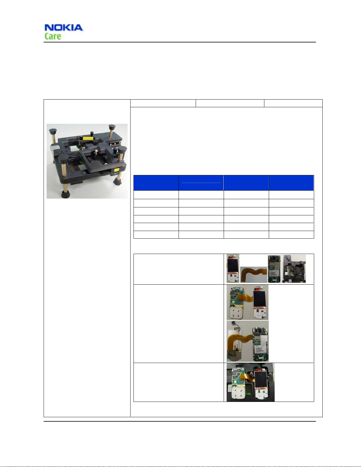
MJ-195 Module Jig
The module jig offers engine module component level repair and analysis.
Features:
connection interfaces for CDMA antenna
galvanic connection to engine module test pads
lid interconnection with test points for measurements
connection to Displays, earpiece, headset and speakers
Band (mid.
ch.)
CDMA 800 TX
CDMA 800 RX
CDMA 1900 TX 600
CDMA 1900 RX 600
GPS
Bluetooth 39
Channel Frequency
/MHz
384
384
836.52
881.52
1880 0.8+/- 0.05
1960 0.8+/- 0.05
1575.42 0.7+/- 0.05
2441 1+/- 0.05
Attenuation
Loss / dB
0.6+/- 0.05
0.6+/- 0.05
MJ set-up instruction:
1. Ready for LCM module+UI
board, jig FPC, main board and
MJ-195
, , ,
2. Connect LCM module+UI board
and main board using jig FPC
(front)
(back)
3. Unfold the MJ-195 and put 2 on
the unfolded MJ-195
Page 2-4 Company Confidential Issue1
Copyright © 2009 Nokia. All rights reserved.
Page 23
RM-384
Service Tools and Service Concepts
4. Close MJ-195. Then please follow
“service concept” to start further
testing.
Table 9 MJ-195 attenuation table
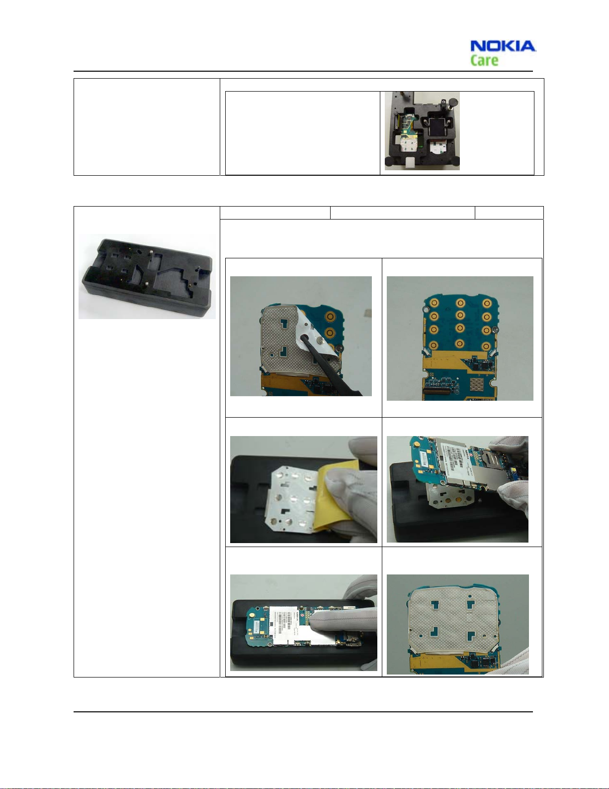
SS-175
SS-175 is a jig to align the adhesive dome sheet assembly onto the PWB in
the proper location during dome sheet replacement.
Domesheet UG:
Dome sheet exchange instruction (a)
Use tweezers to peel the dome shee t.
Dome sheet Alignment Jig
Dome sheet exchange instruction (b)
Remove the dome sheet .
Note: After using the heatgun, the dome sheet
needs to be replaced.
Dome sheet exchange instruction (c)
Place a new dome sheet to dome sheet jig.
Dome sheet exchange instruction (e)
Press firmly on the PWB to ensure correct bonding
of dome sheet.
Table 10 SS-175 attenuation table
Dome sheet exchange instruction (d)
Align the guide pins and place the PWB on the jig
Dome sheet exchange instruction (f)
Inspect to ensure proper adhesion of dome sheet to
PWB.
Issue1 Company Confidential Page 2-5
Copyright © 2009 Nokia. All rights reserved.
Page 24
RM-384
Service Tools and Service Concept
General tools
The table below gives a short overview of service tools that can be used for testing error analysis and repair of
product RM-384.
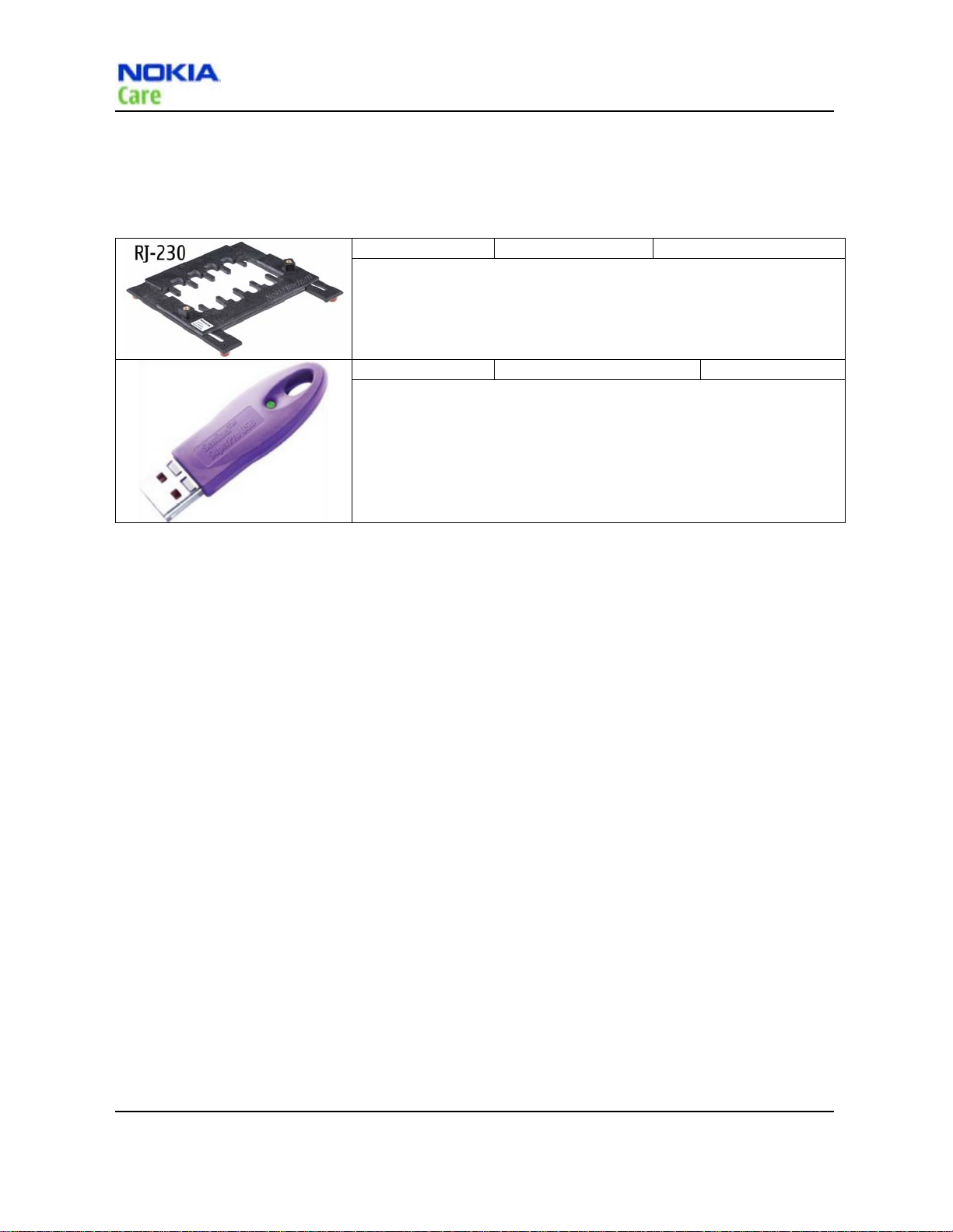
RJ-230 Soldering
RJ-230 is a jig to support component level exchange with soldering
machines for the engine module.
PK-83
PK-83 is a hardware protection key with a USB interface to enable the use
of the service software when connected to the USB port of the PC or
Notebook. It is not possible to use the service software without PK-83
Table 11 General tools table
AMS SW Protection Key (USB)
Page 2-6 Company Confidential Issue1
Copyright © 2009 Nokia. All rights reserved.
Page 25
RM-384
Service Tools and Service Concepts
Cables
The table below gives a short overview of service tools that can be used for testing, error analysis and repair of
product RM-384.
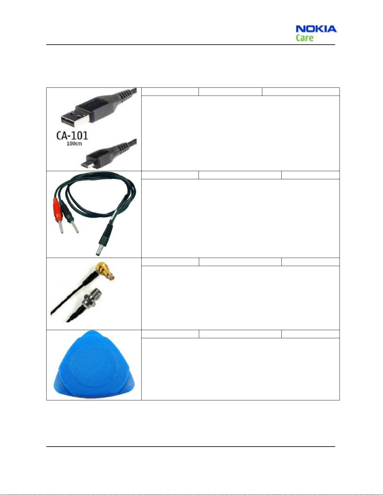
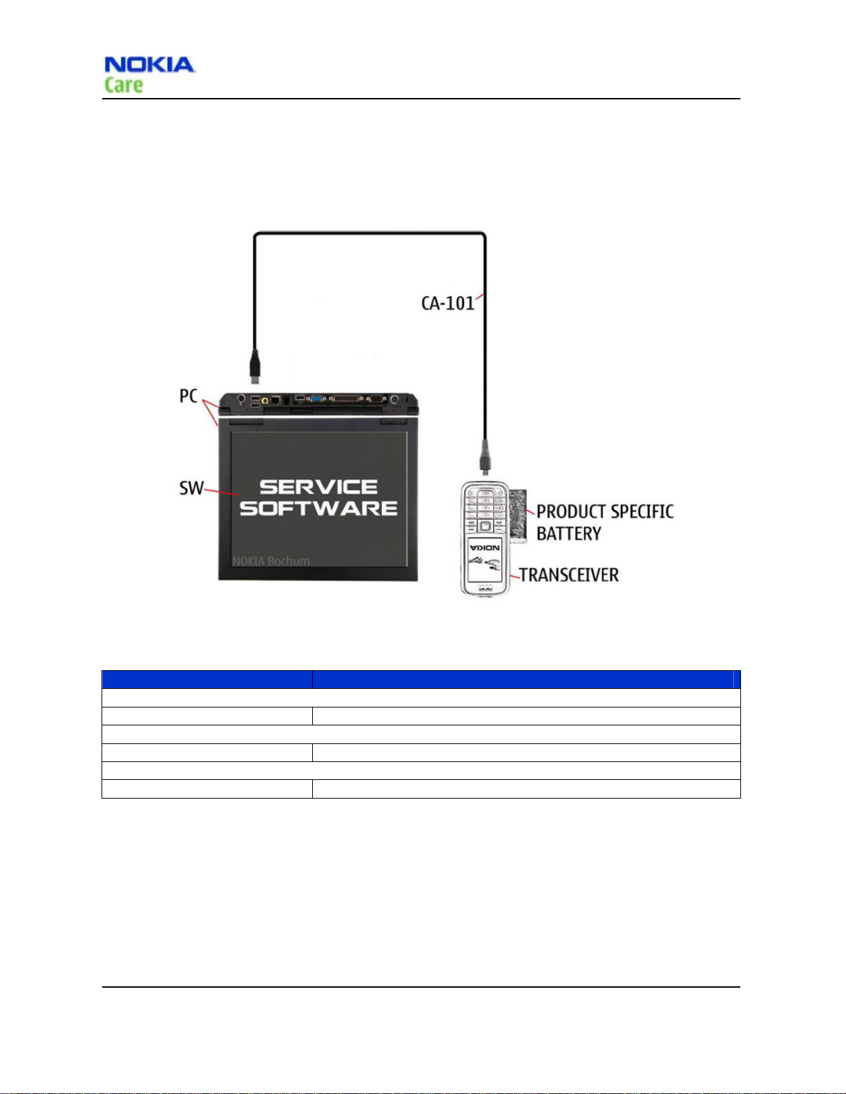
CA-101 Micro USB cable
The CA-101 is a USB-to-micro USB data cable that allows connections
between the PC and the phone.
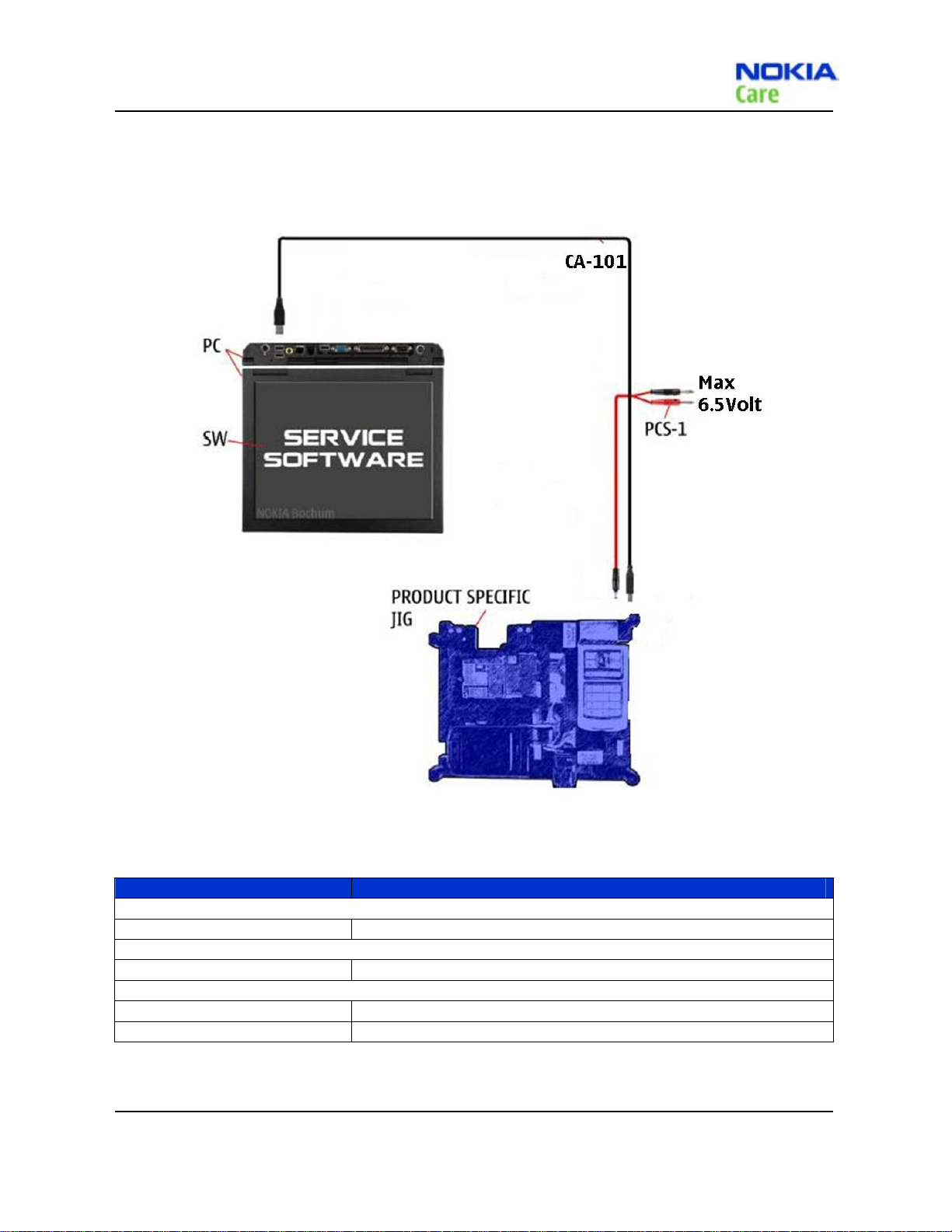
PCS-1 Power Service Cable
The PCS-1 power cable (DC) is used with a docking station, a module jig or
a control unit to supply a controlled voltage.
CA-128RS RF Test Cable
RF Test Cable for use with a Module Jig.
CA-128RS RF cable allow RF function tests and RF tuning in CDMA Cell and
PCS bands.
Features include:
most accurate RF connection to phone module under test
low attenuation and small “ripple” over the width of each band
Note: The RF Test Cable must be used for RF tuning.
SRT-6 Opening tool
SRT-6 is used to open phone covers.
Table 12 Service tools table
Issue1 Company Confidential Page 2-7
Copyright © 2009 Nokia. All rights reserved.
Page 26
Service concepts
POS (Point of Sale) flash concept
RM-384
Service Tools and Service Concept
Figure 1 POS flash concept
Type Description
Product specific tools
BL-4C Battery
Other tools
Nokia Care Suite PC with Nokia Care Suite service software
Cables
CA-101 Micro USB cable
Table 13 POW flash equipments
Page 2-8 Company Confidential Issue1
Copyright © 2009 Nokia. All rights reserved.
Page 27
RM-384
Service Tools and Service Concepts
Flash concept with Module Jig
Figure 2 Flash concept with Module Jig
Type Description
Product specific tools
MJ-195 Module Jig
Other tools
Nokia Care Suite PC with Nokia Care Suite service software
Cables
CA-101 Micro USB cable
PCS-1 Power Service Cable
Table 14 Flash with module jig equipments
Issue1 Company Confidential Page 2-9
Copyright © 2009 Nokia. All rights reserved.
Page 28
Covers-off BB/RF Troubleshooting using Module Jig
RM-384
Service Tools and Service Concept
CA-128RS
CA-128RS
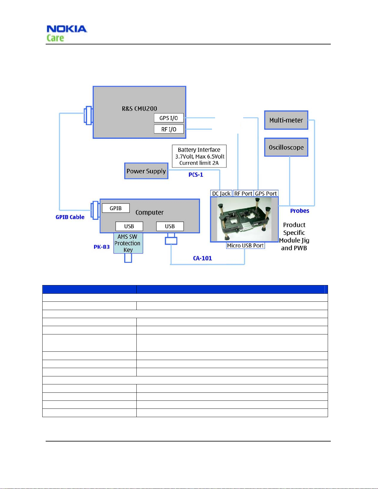
Figure 3 Cover-off BB/RF Troubleshooting using Module Jig
Type Description
Product specific tools
MJ-195 Module Jig
Other tools
PK-83 AMS SW Protection Key (USB)
Nokia Care Suite PC with Nokia Care Suite service software (L3 version)
R&S CMU200 with B89/PK800
module; Agilent8960
Oscilloscope
Multi-meter
Probes used with Oscilloscope and Multi-meter
Cables
CA-101 Micro USB cable
PCS-1 Power Service Cable
CA-128RS RF Test Cable
GPIB Cable
Table 15
CDMA CALL BOX
Covers-off BB/RF Troubleshooting equipments
Page 2-10 Company Confidential Issue1
Copyright © 2009 Nokia. All rights reserved.
Page 29
RM-384
Service Tools and Service Concepts
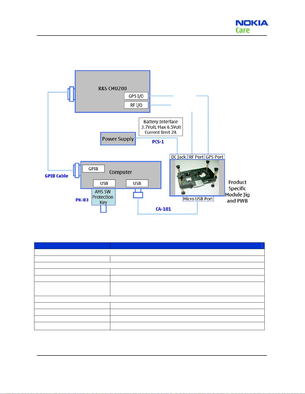
Automated Tuning and Alignment concept
CA-128RS
CA-128RS
Figure 4 Automated Tuning and Alignment concept
Type Description
Product specific tools
MJ-195 Module Jig
Other tools
PK-83 AMS SW Protection Key (USB)
Nokia Care Suite PC with Nokia Care Suite service software (L3 version)
R&S CMU200 with B89/PK800
module; Agilent8960
Cables
CA-101 Micro USB cable
PCS-1 Power Service Cable
CA-128RS RF Test Cable
Table 16 Automated Tuning and Alignment equipments
CDMA CALL BOX
GPIB Cable
Issue1 Company Confidential Page 2-11
Copyright © 2009 Nokia. All rights reserved.
Page 30

(This page left intentionally blank.)
RM-384
Service Tools and Service Concept
Page 2-12 Company Confidential Issue1
Copyright © 2009 Nokia. All rights reserved.
Page 31

Nokia Customer Care
3- Baseband
Troubleshooting
Issue1 Company Confidential Page 3-1
Copyright © 2009 Nokia. All rights reserved.
Page 32

(This page left intentionally blank.)
RM-384
Service Tools and Service Concept
Page 3-2 Company Confidential Issue1
Copyright © 2009 Nokia. All rights reserved.
Page 33

RM-384
Baseband Troubleshooting
Table of Contents
Troubleshooting overview ..................................................................................................................................................................... 3-5
Power on Faults troubleshooting ................................................................................................................................................... 3-12
Display Faults troubleshooting ......................................................................................................................................................... 3-15
Keypad Backlight Faults troubleshooting .................................................................................................................................. 3-17
Keypad Faults troubleshooting ......................................................................................................................................................... 3-19
Hall Sensor Faults troubleshooting ................................................................................................................................................. 3-21
Touch Sensor Faults troubleshooting ........................................................................................................................................... 3-23
Camera Faults troubleshooting ........................................................................................................................................................ 3-25
Flash LED Faults troubleshooting..................................................................................................................................................... 3-28
Vibrator Faults troubleshooting ....................................................................................................................................................... 3-30
Charging Faults troubleshooting ..................................................................................................................................................... 3-32
Speaker Faults troubleshooting ....................................................................................................................................................... 3-35
Receiver Faults troubleshooting ....................................................................................................................................................... 3-38
Microphone Faults troubleshooting .............................................................................................................................................. 3-40
Earphone Faults troubleshooting ................................................................................................................................................... 3-42
RUIM Faults troubleshooting .............................................................................................................................................................. 3-44
FM Fault _Headset not detected troubleshooting ................................................................................................................. 3-46
FM Fault _Can not execute FM radio function troubleshooting .................................................................................... 3-47
FM Fault _Can not hear FM radio from earphone troubleshooting ............................................................................ 3-48
IR proximity troubleshooting ............................................................................................................................................................ 3-50
IR proximity troubleshooting ............................................................................................................................................................ 3-51
IR proximity troubleshooting ............................................................................................................................................................ 3-52
IR proximity troubleshooting ............................................................................................................................................................ 3-53
Issue1 Company Confidential Page 3-3
Copyright © 2009 Nokia. All rights reserved.
Page 34

RM-384
Baseband Troubleshooting
List of Figures
Figure 13 Test components Location of display faults ................................................................................................... 3-16
Figure 14 Test components Location of keypad backlight faults ........................................................................... 3-18
Figure 15 Test components Location of keypad faults .................................................................................................. 3-20
Figure 16 Test components Location of hall sensor faults .......................................................................................... 3-22
Figure 17 Test components Location of touch sensor faults ..................................................................................... 3-24
Figure 18 Test components Location of camera faults -1 ............................................................................................ 3-26
Figure 19 Test components Location of camera faults - 2 ........................................................................................... 3-27
Figure 20 Test components Location of flash LED faults ............................................................................................... 3-29
Figure 21 Test components Location of vibrator faults ................................................................................................. 3-31
Figure 22 Test components Location of charging faults -1 ........................................................................................ 3-33
Figure 23 Test components Location of charging faults -2 ........................................................................................ 3-34
Figure 24 Test components Location of speaker faults -1 ........................................................................................... 3-36
Figure 25 Test components Location of speaker faults -2 ........................................................................................... 3-37
Figure 26 Test components Location of receiver faults ................................................................................................. 3-39
Figure 27 Test components Location of microphone faults ...................................................................................... 3-41
Figure 28 Test components Location of earphone faults ............................................................................................ 3-43
Figure 29 Test components Location of RUIM faults ....................................................................................................... 3-45
Figure 30 Test components Location of FM faults ............................................................................................................ 3-49
Figure 31 Test components Location of Rec_FPC Component Placement ........................................................ 3-55
Figure 32 Test components Location of A-cover assembly ........................................................................................ 3-56
Figure 33 Test components Location of IR-2: Pad peel off .......................................................................................... 3-57
Page 3-4 Company Confidential Issue1
Copyright © 2009 Nokia. All rights reserved.
Page 35

RM-384
Baseband Troubleshooting
Troubleshooting overview
For practical reasons, troubleshooting is divided into two sections;
Baseband troubleshooting, including camera, GPS and Bluetooth
RF troubleshooting
Issue1 Company Confidential Page 3-5
Copyright © 2009 Nokia. All rights reserved.
Page 36

General RF troubleshooting
PWB top side
MIC 1
RM-384
Baseband Troubleshooting
T flash connect
Flash LED
Phone jack
CL6100 IC
(Mp3 decode/encode ) IC
Combo memory
MSM6800A-3
Side key
MIC 2
Figure 5 PWB top side
Page 3-6 Company Confidential Issue1
Copyright © 2009 Nokia. All rights reserved.
Page 37

RM-384
Baseband Troubleshooting
PWB bottom side
Music key LED
OVP IC
Flash LED
driver IC
LP3919RLX-B (PMIC)
Audio DAC IC
LCD Backlight
driver IC
Keypad & music
key LED driver IC
Music key LED
Figure 6 PWB bottom side
Issue1 Company Confidential Page 3-7
Copyright © 2009 Nokia. All rights reserved.
Page 38

UI Board side
RM-384
Baseband Troubleshooting
Figure 7 UI Board side
Page 3-8 Company Confidential Issue1
Copyright © 2009 Nokia. All rights reserved.
Page 39

RM-384
Baseband Troubleshooting
PCB placement
Figure 8 PCB placement
Issue1 Company Confidential Page 3-9
Copyright © 2009 Nokia. All rights reserved.
Page 40

PCB UI Board Placement
RM-384
Baseband Troubleshooting
Figure 9 PCB UI board placement
Page 3-10 Company Confidential Issue1
Copyright © 2009 Nokia. All rights reserved.
Page 41

RM-384
Baseband Troubleshooting
Power on sequence
Figure 10 Power on sequence
Issue1 Company Confidential Page 3-11
Copyright © 2009 Nokia. All rights reserved.
Page 42

Power on Faults troubleshooting
Troubleshooting flow
RM-384
Baseband Troubleshooting
Page 3-12 Company Confidential Issue1
Copyright © 2009 Nokia. All rights reserved.
Page 43

RM-384
Baseband Troubleshooting
Test Components Location - 1
Figure 11 Test component location of power on faults
Issue1 Company Confidential Page 3-13
Copyright © 2009 Nokia. All rights reserved.
Page 44

Test Components Location - 2
RM-384
Baseband Troubleshooting
Figure 12 Test component location of power on faults
Page 3-14 Company Confidential Issue1
Copyright © 2009 Nokia. All rights reserved.
Page 45

RM-384
Baseband Troubleshooting
Display Faults troubleshooting
Troubleshooting flow
Issue1 Company Confidential Page 3-15
Copyright © 2009 Nokia. All rights reserved.
Page 46

Test components Location
RM-384
Baseband Troubleshooting
Figure 13 Test component location of display faults
Page 3-16 Company Confidential Issue1
Copyright © 2009 Nokia. All rights reserved.
Page 47

RM-384
Baseband Troubleshooting
Keypad Backlight Faults troubleshooting
Troubleshooting flow
Issue1 Company Confidential Page 3-17
Copyright © 2009 Nokia. All rights reserved.
Page 48

Test components Location
RM-384
Baseband Troubleshooting
Figure 14 Test component location of keypad backlight faults
Page 3-18 Company Confidential Issue1
Copyright © 2009 Nokia. All rights reserved.
Page 49

RM-384
Baseband Troubleshooting
Keypad Faults troubleshooting
Troubleshooting flow
Issue1 Company Confidential Page 3-19
Copyright © 2009 Nokia. All rights reserved.
Page 50

Test components Location
RM-384
Baseband Troubleshooting
Figure 15 Test component location of keypad faults
Page 3-20 Company Confidential Issue1
Copyright © 2009 Nokia. All rights reserved.
Page 51

RM-384
Baseband Troubleshooting
Hall Sensor Faults troubleshooting
Troubleshooting flow
Issue1 Company Confidential Page 3-21
Copyright © 2009 Nokia. All rights reserved.
Page 52

Test components Location
RM-384
Baseband Troubleshooting
Figure 16 Test component location of hall sensor faults
Page 3-22 Company Confidential Issue1
Copyright © 2009 Nokia. All rights reserved.
Page 53

RM-384
Baseband Troubleshooting
Touch Sensor Faults troubleshooting
Troubleshooting flow
Issue1 Company Confidential Page 3-23
Copyright © 2009 Nokia. All rights reserved.
Page 54

Test components Location
RM-384
Baseband Troubleshooting
Figure 17 Test component location of touch sensor faults
Page 3-24 Company Confidential Issue1
Copyright © 2009 Nokia. All rights reserved.
Page 55

RM-384
Baseband Troubleshooting
Camera Faults troubleshooting
Troubleshooting flow
Issue1 Company Confidential Page 3-25
Copyright © 2009 Nokia. All rights reserved.
Page 56

Test components Location 1
RM-384
Baseband Troubleshooting
Figure 18 Test component location of camera faults
Page 3-26 Company Confidential Issue1
Copyright © 2009 Nokia. All rights reserved.
Page 57

RM-384
Baseband Troubleshooting
Test components Location 2
Figure 19 Test component location of camera faults
Issue1 Company Confidential Page 3-27
Copyright © 2009 Nokia. All rights reserved.
Page 58

Flash LED Faults troubleshooting
Troubleshooting flow
RM-384
Baseband Troubleshooting
Page 3-28 Company Confidential Issue1
Copyright © 2009 Nokia. All rights reserved.
Page 59

RM-384
Baseband Troubleshooting
Test components Location
Figure 20 Test component location of flash LED faults
Issue1 Company Confidential Page 3-29
Copyright © 2009 Nokia. All rights reserved.
Page 60

Vibrator Faults troubleshooting
Troubleshooting flow
RM-384
Baseband Troubleshooting
Page 3-30 Company Confidential Issue1
Copyright © 2009 Nokia. All rights reserved.
Page 61

RM-384
Baseband Troubleshooting
Test components Location
Figure 21 Test component location of vibrator faults
Issue1 Company Confidential Page 3-31
Copyright © 2009 Nokia. All rights reserved.
Page 62

Charging Faults troubleshooting
Troubleshooting flow
RM-384
Baseband Troubleshooting
Page 3-32 Company Confidential Issue1
Copyright © 2009 Nokia. All rights reserved.
Page 63

RM-384
Baseband Troubleshooting
Test components Location 1
Figure 22 Test component location of charging faults
Issue1 Company Confidential Page 3-33
Copyright © 2009 Nokia. All rights reserved.
Page 64

Test components Location 2
RM-384
Baseband Troubleshooting
Figure 23 Test component location of charging faults
Page 3-34 Company Confidential Issue1
Copyright © 2009 Nokia. All rights reserved.
Page 65

RM-384
Baseband Troubleshooting
Speaker Faults troubleshooting
Troubleshooting flow
Issue1 Company Confidential Page 3-35
Copyright © 2009 Nokia. All rights reserved.
Page 66

Test components Location 1
RM-384
Baseband Troubleshooting
Figure 24 Test component location of speaker faults
Page 3-36 Company Confidential Issue1
Copyright © 2009 Nokia. All rights reserved.
Page 67

RM-384
Baseband Troubleshooting
Test components Location 2
Figure 25 Test component location of speaker faults
Issue1 Company Confidential Page 3-37
Copyright © 2009 Nokia. All rights reserved.
Page 68

Receiver Faults troubleshooting
Troubleshooting flow
RM-384
Baseband Troubleshooting
Page 3-38 Company Confidential Issue1
Copyright © 2009 Nokia. All rights reserved.
Page 69

RM-384
Baseband Troubleshooting
Test components Location
Figure 26 T e st component location of receiv er faults
Issue1 Company Confidential Page 3-39
Copyright © 2009 Nokia. All rights reserved.
Page 70

Microphone Faults troubleshooting
Troubleshooting flow
RM-384
Baseband Troubleshooting
Page 3-40 Company Confidential Issue1
Copyright © 2009 Nokia. All rights reserved.
Page 71

RM-384
Baseband Troubleshooting
Test components Location
Figure 27 Test component location of microphone faults
Issue1 Company Confidential Page 3-41
Copyright © 2009 Nokia. All rights reserved.
Page 72

Earphone Faults troubleshooting
Troubleshooting flow
RM-384
Baseband Troubleshooting
Page 3-42 Company Confidential Issue1
Copyright © 2009 Nokia. All rights reserved.
Page 73

RM-384
Baseband Troubleshooting
Test components Location
Figure 28 Test component location of earphone faults
Issue1 Company Confidential Page 3-43
Copyright © 2009 Nokia. All rights reserved.
Page 74

RUIM Faults troubleshooting
Troubleshooting flow
RM-384
Baseband Troubleshooting
Page 3-44 Company Confidential Issue1
Copyright © 2009 Nokia. All rights reserved.
Page 75

RM-384
Baseband Troubleshooting
Test components Location
Figure 29 Test component location of RUIM faults
Issue1 Company Confidential Page 3-45
Copyright © 2009 Nokia. All rights reserved.
Page 76

FM Fault _Headset not detected troubleshooting
Troubleshooting flow
RM-384
Baseband Troubleshooting
Page 3-46 Company Confidential Issue1
Copyright © 2009 Nokia. All rights reserved.
Page 77

RM-384
Baseband Troubleshooting
FM Fault _Can not execute FM radio function troubleshooting
Troubleshooting flow
Issue1 Company Confidential Page 3-47
Copyright © 2009 Nokia. All rights reserved.
Page 78

Baseband Troubleshooting
FM Fault _Can not hear FM radio from earphone troubleshooting
Troubleshooting flow
RM-384
Page 3-48 Company Confidential Issue1
Copyright © 2009 Nokia. All rights reserved.
Page 79

RM-384
Baseband Troubleshooting
Test components Location
Figure 30 Test component location of FM faults
Issue1 Company Confidential Page 3-49
Copyright © 2009 Nokia. All rights reserved.
Page 80

IR proximity troubleshooting
Troubleshooting flow
RM-384
Baseband Troubleshooting
Page 3-50 Company Confidential Issue1
Copyright © 2009 Nokia. All rights reserved.
Page 81

RM-384
Baseband Troubleshooting
IR proximity troubleshooting
Troubleshooting flow
Issue1 Company Confidential Page 3-51
Copyright © 2009 Nokia. All rights reserved.
Page 82

IR proximity troubleshooting
Troubleshooting flow
RM-384
Baseband Troubleshooting
Page 3-52 Company Confidential Issue1
Copyright © 2009 Nokia. All rights reserved.
Page 83

RM-384
Baseband Troubleshooting
IR proximity troubleshooting
Troubleshooting flow
Issue1 Company Confidential Page 3-53
Copyright © 2009 Nokia. All rights reserved.
Page 84

Page 85

RM-384
Baseband Troubleshooting
Test components Location- Rec_FPC Component Placement
Figure 31 Test component location of Rec_FPC Component
Issue1 Company Confidential Page 3-55
Copyright © 2009 Nokia. All rights reserved.
Page 86

Test components Location - A-cover assembly
RM-384
Baseband Troubleshooting
Figure 32 IR-1: A-cover assembly
Page 3-56 Company Confidential Issue1
Copyright © 2009 Nokia. All rights reserved.
Page 87

RM-384
Baseband Troubleshooting
Test components Location - A-cover assembly
Figure IR-2 Pad Peel off
Figure 33 IR-2: Pad peel off
Issue1 Company Confidential Page 3-57
Copyright © 2009 Nokia. All rights reserved.
Page 88

(This page left intentionally blank.)
RM-384
Baseband Troubleshooting
Page 3-58 Company Confidential Issue1
Copyright © 2009 Nokia. All rights reserved.
Page 89

Nokia Customer Care
4- RF Troubleshooting
Issue1 Company Confidential Page 4-1
Copyright © 2008 Nokia. All rights reserved.
Page 90

(This page left intentionally blank.)
RM-384
RF Troubleshooting
Page 4-2 Company Confidential Issue1
Copyright © 2008 Nokia. All rights reserved.
Page 91

RM-384
RF Troubleshooting
Table of Contents
General RF troubleshooting ................................................................................................................................................................... 4-4
Receiver troubleshooting ..................................................................................................................................................................... 4-14
GPS troubleshooting ................................................................................................................................................................................ 4-20
Bluetooth Troubleshooting ................................................................................................................................................................. 4-22
List of Tables
Table 17 RF TX voltage checking point information ........................................................................................................... 4-11
Table 18 Cell band Tx check shows the test points shown in Figure 41. ................................................................ 4-12
Table 19 PCS band Tx check shows the test points shown in Figure 41. ............................................................... 4-12
Table 20 Receiver check from RF to DVGA (Cellular band) ............................................................................................... 4-16
Table 21 Receiver check from RF to DVGA (PCS band) ........................................................................................................ 4-16
Table 22 shows the Tx DC test points shown in Figure 43 .............................................................................................. 4-16
Table 23 Cell band Rx RF troubleshooting test points Shown in Figure 43. ......................................................... 4-17
Table 24 PCS band Rx RF troubleshooting test points Shown in Figure 43. ......................................................... 4-17
Table 25 GPS RF troubleshooting test points Shown in Figure 46. ............................................................................ 4-22
Table 26 BT voltage checking test point ..................................................................................................................................... 4-25
List of Figures
Figure 34 Component Layout (Top) .................................................................................................................................................. 4-5
Figure 35 Component Layout (Bottom) ........................................................................................................................................ 4-6
Figure 36 RF TX key components ....................................................................................................................................................... 4-7
Figure 37 RF RX key components ....................................................................................................................................................... 4-7
Figure 38 Display of Nokia CDMA L3 PST Service Software ................................................................................................. 4-9
Figure 39 Steps of configuring FTM for RF troubleshooting ........................................................................................... 4-10
Figure 40 Tx DC checking test points ............................................................................................................................................. 4-11
Figure 41 Tx RF Test Points .................................................................................................................................................................. 4-12
Figure 42 Steps of configuring FTM for RF Troubleshooting .......................................................................................... 4-15
Figure 43 RF RX voltage checking test point ............................................................................................................................ 4-17
Figure 44 GPS system block diagram ........................................................................................................................................... 4-20
Figure 45 RF Toolkit setup for GPS troubleshooting ............................................................................................................ 4-20
Figure 46 RF GPS checking test point ............................................................................................................................................ 4-21
Figure 47 BT system block diagram .............................................................................................................................................. 4-23
Figure 48 Display of entering the Bluetooth test mode ................................................................................................... 4-24
Figure 49 RF GPS checking test point ............................................................................................................................................ 4-25
Issue1 Company Confidential Page 4-3
Copyright © 2008 Nokia. All rights reserved.
Page 92

RM-384
RF Troubleshooting
General RF troubleshooting
Introduction to RF troubleshooting
Most RF semiconductors are static discharge sensitive
ESD protection must be applied during repair (ground straps and ESD soldering irons).
Pre-baking
These parts are moisture sensitive and must be pre-baked prior to soldering:
RFIC: Qualcomm MSM6800A at U301
PA: AWT6307R at U201,AWT6308R at U204
Discrete components
In addition to the key-components, there are a number of discrete components (resistors, inductors and
capacitors) for which troubleshooting is done mainly by
Capacitors: check for short circuits.
Resistors: check value with an ohm meter.
Note: In-circuit measurements should be evaluated carefully
visual inspection.
Measuring equipment
All measurements should be done using:
An oscilloscope for low frequency and DC measurements. Recommended probe: 10:1, 10Mohm//8pF.Title of
the Document + Issue Number/Date of publication
A radio communication tester including RF generator and spectrum analyser, for example Rohde & Schwarz
CMU200. (Alternatively a spectrum analyser and an RF generator can be used. Some tests in this guide are not
possible to perform if this solution is chosen).
Note: All measurements with an RF coupler should be performed in an RF-shielded environment because
nearby base stations can disturb sensitive receiver measurements. If there is no possibility to use RF
shielded environment, testing at frequencies of nearby base stations should be avoided.
Level of repair
The scope of this guideline is to enable repairs at key-component level. Some key-components are not
accessible, i.e. not replaceable.
Page 4-4 Company Confidential Issue1
Copyright © 2008 Nokia. All rights reserved.
Page 93

RM-384
p
RF Troubleshooting
RF key components
BT/FM Module
GPS Antenna
RF connector for
GPS
GPS Rx Saw filter
32.768KHz Crystal
19.2MHz XTA L
BT Antenna feed point
MSM6800
RFR 6500
Power Detector
PCS coupler
Cell coupler
GPS Rx Saw filter
Cell Rx Saw filter
PCS Rx Saw filter
PCS Du
lexer
PCS PA M
PCS Tx Saw filter
Cell Tx Saw filter
Cell PAM
Cell Duplexer
Diplexer
RF connector for
Cell & PCS
RF Antenna feed point
Figure 34 Component Layout (Top)
Issue1 Company Confidential Page 4-5
Copyright © 2008 Nokia. All rights reserved.
Page 94

RM-384
RF Troubleshooting
Figure 35 Component Layout (Bottom)
Page 4-6 Company Confidential Issue1
Copyright © 2008 Nokia. All rights reserved.
Page 95

RM-384
RF Troubleshooting
RF TX key components
RF RX key components
Figure 36 RF TX key components
Figure 37 RF RX key components
Issue1 Company Confidential Page 4-7
Copyright © 2008 Nokia. All rights reserved.
Page 96

Troubleshooting flow
RM-384
RF Troubleshooting
Page 4-8 Company Confidential Issue1
Copyright © 2008 Nokia. All rights reserved.
Page 97

RM-384
RF Troubleshooting
RF Call Test in Nokia CDMA L3 PST Fx.x
Context
Always start the troubleshooting procedure by running the RF Call Test in Nokia CDMA L3 PST. If a test fails, please
follow the diagram below.
If the phone is dead and you cannot perform the self tests, go to Dead or jammed device troubleshooting
in the baseband troubleshooting section.
Setup for RF Troubleshooting
Use the following steps to configure FTM mode for RF troubleshooting.
1. Connect RF connector to a spectrum
2. Put PWB on the module jig, connect data service cable between PC and Module Jig and connect a power
supply
3. Launch Nokia CDMA L3 PST Fx.x Service Software and run RF Toolkit function
4. The RF and Testing box appears
5. Select “RF and Testing “.
6. Press “Start RF Connection”
Figure 38 Display of Nokia CDMA L3 PST Service Software
Issue1 Company Confidential Page 4-9
Copyright © 2008 Nokia. All rights reserved.
Page 98

Setup for TX Troubleshooting
Use the following steps to configure FTM for RF troubleshooting.
1. Connect RF test connector to a CMU200.
2. Connect the mobile terminal to PC via the Module Jig, and connect a power supply.
3. Open RF Toolkit in L3 program. The RF Toolkit appears.
4. Click “Start RF connection” in connection.
5. Select “FTM” in phone mode setting and click “set mode” .
6. Select band mode “Cellular band/PCS band” in band setting and
click “Set band” .
7. Set a channel “384/600” in RF channel setting and click “Set channel” .
Cellular Band Test channel : 384
PCS Band Test channel : 600
8. Select “On” in TX on/off and click “set Tx On/off” .
9. Select “Off” in waveform and click “Set waveform”.
10. Select “0 - R0_On R1_On” in PA Range and lick “Set PA Range”.
11. Set “110” in AGC and click “set AGC”.
12. After finish above checking, select “Online” in “ phone mode setting” and
click “Set phone mode”.
RM-384
RF Troubleshooting
Figure 39 Steps of configuring FTM for RF troubleshooting
Page 4-10 Company Confidential Issue1
Copyright © 2008 Nokia. All rights reserved.
Page 99

RM-384
RF Troubleshooting
RF TX voltage checking
Steps
1. Set up the main board in the module jig.
2. Check the following:
# Signal name Test point Voltage (all bands)
1 TX_2.85V U403 2.85V
2 MSMP_2.6V U403 2.6V
3 TX_ON U403,U301 2.6V
4 PA_RXX U403,U301 0V for high gain mode 2.4~2.5V for low gain mode
5 PA_ON0 U403,U301 2.5~2.6V for PA turning on, 0V for turning off (CELL)
6 PA_ON1 U403,U301 2.5~2.6V for PA turning on, 0V for turning off ( PCS)
Table 17 RF TX voltage checking point information
Figure 40 Tx DC checking test points
Issue1 Company Confidential Page 4-11
Copyright © 2008 Nokia. All rights reserved.
Page 100

TX RF Test Points
RM-384
RF Troubleshooting
Figure 41 Tx RF Test Points
Test
Point
1 TX_AGC_ADJ 1.85V for 5 dBm, 2.1V for 15 dBm U202
2 RFT6150 output -17 ~ -10 dBm U202
3 Cellular SAW output Max atten 7dB SAW201
4 Cellular PA output Gain 5~15dB U201
5 Cellular Coupler Output Max atten 7dB U207
6 Cellular Duplexer Output Max atten 3dB DPX102
7 Diplexer Out Max atten 3dB DPX101
13 RF connector 20 dBm J100
Test
Point
8 RFT6150 output -18 ~ -12 dBm U202
9 PCS PCS SAW output Max atten 7dB SAW202
10 PCS PA output Gain 5~15dB U204
11 PCS Coupler Output Max atten 3dB U208
12 PCS Duplexer Output Max atten 3dB DPX103
7 Diplexer Out Max atten 3dB DPX101
13 RF connector 19 dBm J100
Description Value
Table 18 Cell band Tx check shows the test points shown in Figure 41.
Description Value
Table 19 PCS band Tx check shows the test points shown in Figure 41.
Check
component
Check
component
Page 4-12 Company Confidential Issue1
Copyright © 2008 Nokia. All rights reserved.
 Loading...