

Page 1

Nokia Customer Care
Service Manual
RM-376 (Nokia 2608)
Mobile Terminal
Part No: (Issue 1)
COMPANY CONFIDENTIAL
Company Confidential
Copyright © 2009 Nokia Corporation. All rights reserved.
Page 2
Amendment Record Sheet
Amendment Record Sheet
Amendment No Date Inserted By Comments
Issue 1 06/2008 Shelly Wang
09/2008 Shelly Wang update
01/2009 Alex Huang Add product selection part
RM-376
Page II Company Confidential Issue 1
Copyright © 2009 Nokia. All rights reserved.
Page 3

RM-376
Copyright
Copyright
Copyright © 2008 Nokia. All rights reserved.
Reproduction, transfer, distribution or storage of part or all of the contents in this document in any form without the
prior written permission of Nokia is prohibited.
Nokia, Nokia Connecting People, and Nokia X and Y are trademarks or registered trademarks of Nokia
Corporation. Other product and company names mentioned herein may be trademarks or tradenames of their
respective owners.
Nokia operates a policy of continuous development. Nokia reserves the right to make changes and improvements
to any of the products described in this document without prior notice.
Under no circumstances shall Nokia be responsible for any loss of data or income or any special, incidental,
consequential or indirect damages howsoever caused.
The contents of this document are provided "as is". Except as required by applicable law, no warranties of any kind,
either express or implied, including, but not limited to, the implied warranties of merchantability and fitness for a
particular purpose, are made in relation to the accuracy, reliability or contents of this document. Nokia reserves the
right to revise this document or withdraw it at any time without prior notice.
The availability of particular products may vary by region.
IMPORTANT
This document is intended for use by qualified service personnel only.
Issue1 Company Confidential Page III
Copyright © 2009 Nokia. All rights reserved.
Page 4

RM-376
Warnings and cautions
Warnings and cautions
Warnings
z IF THE DEVICE CAN BE INSTALLED IN A VEHICLE, CARE MUST BE TAKEN ON INSTALLATION IN
VEHICLES FITTED WITH ELECTRONIC ENGINE MANAGEMENT SYSTEMS AND ANTI-SKID BRAKING
SYSTEMS. UNDER CERTAIN FAULT CONDITIONS, EMITTED RF ENERGY CAN AFFECT THEIR
OPERATION. IF NECESSARY, CONSULT THE VEHICLE DEALER/ MANUFACTURER TO DETERMINE
THE IMMUNITY OF VEHICLE ELECTRONIC SYSTEMS TO RF ENERGY.
z THE PRODUCT MUST NOT BE OPERATED IN AREAS LIKELY TO CONTAIN POTENTIALLY EXPLOSIVE
ATMOSPHERES, FOR EXAMPLE, PETROL STATIONS (SERVICE STATIONS), BLASTING AREAS ETC.
z OPERATION OF ANY RADIO TRANSMITTING EQUIPMENT, INCLUDING CELLULAR TELEPHONES,
MAY INTERFERE WITH THE FUNCTIONALITY OF INADEQUATELY PROTECTED MEDICAL DEVICES.
CONSULT A PHYSICIAN OR THE MANUFACTURER OF THE MEDICAL DEVICE IF YOU HAVE ANY
QUESTIONS. OTHER ELECTRONIC EQUIPMENT MAY ALSO BE SUBJECT TO INTERFERENCE.
z BEFORE MAKING ANY TEST CONNECTIONS, MAKE SURE YOU HAVE SWITCHED OFF ALL
EQUIPMENT.
Cautions
z Servicing and alignment must be undertaken by qualified personnel only.
z Ensure all work is carried out at an anti-static workstation and that an anti-static wrist strap is worn.
z Ensure solder, wire, or foreign matter does not enter the telephone as damage may result.
z Use only approved components as specified in the parts list.
z Ensure all components, modules, screws and insulators are correctly re-fitted after servicing and alignment.
z Ensure all cables and wires are repositioned correctly.
z Never test a mobile phone WCDMA transmitter with full Tx power, if there is no possibility to perform the
measurements in a good performance RF-shielded room. Even low power WCDMA transmitters may disturb
nearby WCDMA networks and cause problems to 3G cellular phone communication in a wide area.
z During testing never activate the GSM or WCDMA transmitter without a proper antenna load, otherwise GSM or
WCDMA PA may be damaged.
Page IV Company Confidential Issue 1
Copyright © 2009 Nokia. All rights reserved.
Page 5

RM-376
ESD protection
ESD protection
Nokia requires that service points have sufficient ESD protection (against static electricity) when servicing the
phone.
Any product of which the covers are removed must be handled with ESD protection. The SIM card can be replaced
without ESD protection if the product is otherwise ready for use.
To replace the covers ESD protection must be applied.
All electronic parts of the product are susceptible to ESD. Resistors, too, can be damaged by static electricity
discharge.
All ESD sensitive parts must be packed in metallized protective bags during shipping and handling outside any
ESD Protected Area (EPA).
Every repair action involving opening the product or handling the product components must be done under ESD
protection.
ESD protected spare part packages MUST NOT be opened/closed out of an ESD Protected Area.
For more information and local requirements about ESD protection and ESD Protected Area, contact your local
Nokia After Market Services representative.
Issue1 Company Confidential Page V
Copyright © 2009 Nokia. All rights reserved.
Page 6

RM-376
Care and maintenance
Care and maintenance
This product is of superior design and craftsmanship and should be treated with care. The suggestions below will
help you to fulfill any warranty obligations and to enjoy this product for many years.
z Keep the phone and all its parts and accessories out of the reach of small children.
z Keep the phone dry. Precipitation, humidity and all types of liquids or moisture can contain minerals that will
corrode electronic circuits.
z Do not use or store the phone in dusty, dirty areas. Its moving parts can be damaged.
z Do not store the phone in hot areas. High temperatures can shorten the life of electronic devices, damage
batteries, and warp or melt certain plastics.
z Do not store the phone in cold areas. When it warms up (to its normal temperature), moisture can form inside,
which may damage electronic circuit boards.
z Do not drop, knock or shake the phone. Rough handling can break internal circuit boards.
z Do not use harsh chemicals, cleaning solvents, or strong detergents to clean the phone.
z Do not paint the phone. Paint can clog the moving parts and prevent proper operation.
z Use only the supplied or an approved replacement antenna. Unauthorised antennas, modifications or
attachments could damage the phone and may violate regulations governing radio devices.
All of the above suggestions apply equally to the product, battery, charger or any accessory.
Page VI Company Confidential Issue 1
Copyright © 2009 Nokia. All rights reserved.
Page 7

RM-376
Company Policy
Company Policy
Our policy is of continuous development; details of all technical modifications will be included with service bulletins.
While every endeavour has been made to ensure the accuracy of this document, some errors may exist. If any
errors are found by the reader, NOKIA MOBILE PHONES Business Group should be notified in writing/email.
Please state:
z Title of the Document + Issue Number/Date of publication
z Latest Amendment Number (if applicable)
z Page(s) and/or Figure(s) in error
Please send to:
NOKIA CORPORATION
Nokia Mobile Phones Business Group
Nokia Customer Care
PO Box 86
FIN-24101 SALO
Finland
E-mail: Service.Manuals@nokia.com
Issue1 Company Confidential Page VII
Copyright © 2009 Nokia. All rights reserved.
Page 8

RM-376
Battery information
Battery information
Note: A new battery's full performance is achieved only after two or three complete charge and discharge
cycles!
The battery can be charged and discharged hundreds of times but it will eventually wear out. When the operating
time (talk-time and standby time) is noticeably shorter than normal, it is time to buy a new battery.
Use only batteries approved by the phone manufacturer and recharge the battery only with the chargers approved
by the manufacturer. Unplug the charger when not in use. Do not leave the battery connected to a charger for
longer than a week, since overcharging may shorten its lifetime. If left unused a fully charged battery will discharge
itself over time.
Temperature extremes can affect the ability of your battery to charge.
For good operation times with Li-Ion batteries, discharge the battery from time to time by leaving the product
switched on until it turns itself off (or by using the battery discharge facility of any approved accessory available for
the product). Do not attempt to discharge the battery by any other means.
Use the battery only for its intended purpose.
Never use any charger or battery which is damaged.
Do not short-circuit the battery. Accidental short-circuiting can occur when a metallic object (coin, clip or pen)
causes direct connection of the + and - terminals of the battery (metal strips on the battery) for example when you
carry a spare battery in your pocket or purse. Short-circuiting the terminals may damage the battery or the
connecting object.
Leaving the battery in hot or cold places, such as in a closed car in summer or winter conditions, will reduce the
capacity and lifetime of the battery. Always try to keep the battery between 15°C and 25°C (59°F and 77°
F). A phone with a hot or cold battery may temporarily not work, even when the battery is fully charged.
Batteries' performance is particularly limited in temperatures well below freezing.
Do not dispose of batteries in a fire!
Dispose of batteries according to local regulations (e.g. recycling). Do not dispose as household waste.
Page VIII Company Confidential Issue 1
Copyright © 2009 Nokia. All rights reserved.
Page 9
RM-376
Nokia 2608 Service Manual Structure
Nokia 2608 Service Manual Structure
1 General Information
2 Service Tools and Service Concepts
3 Baseband Troubleshooting
4 RF troubleshooting
5 System Module and User Interface
6 Glossary
Issue1 Company Confidential Page IX
Copyright © 2009 Nokia. All rights reserved.
Page 10

(This page left intentionally blank.)
RM-376
Nokia 2608 Service Manual Structure
Page X Company Confidential Issue 1
Copyright © 2009 Nokia. All rights reserved.
Page 11

Nokia Customer Care
1- General Information
Issue1 Company Confidential Page 1-1
Copyright © 2009 Nokia. All rights reserved.
Page 12

(This page left intentionally blank.)
RM-376
General Information
Page 1-2 Company Confidential Issue 1
Copyright © 2009 Nokia. All rights reserved.
Page 13

RM-376
General Information
Table of Contents
Product selection ..............................................................................................................................................1-5
Product features and sales packages ............................................................................................................ 1-5
Mobile Enhancement .......................................................................................................................................1-6
Technical specifications....................................................................................................................................1-7
Transceiver general specifications .................................................................................................. 1-7
Main RF characteristics for CDMA2000 Cell band 800................................................................1-7
Battery endurance.............................................................................................................................1-7
Issue1 Company Confidential Page 1-3
Copyright © 2009 Nokia. All rights reserved.
Page 14

(This page left intentionally blank.
RM-376
General Information
Page 1-4 Company Confidential Issue 1
Copyright © 2009 Nokia. All rights reserved.
Page 15
RM-376
General Information
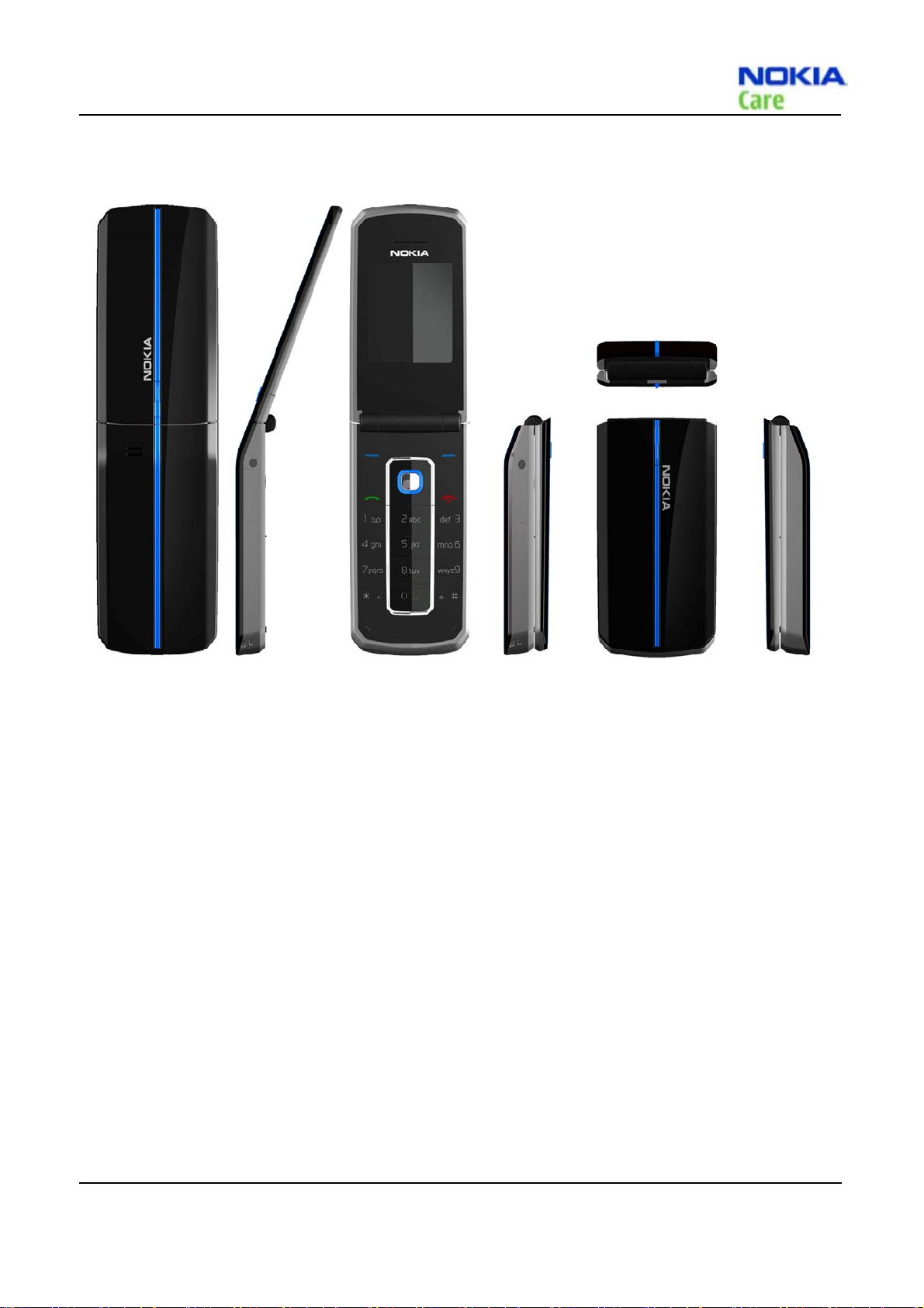
Product selection
RM-376 (Nokia 2608) is a CDMA signal band phone, supporting CDMA2000 1xRTT /Cell band
Figure 1 RM-376 (Nokia 2608) product picture
Product features and sales packages
Hardware features
z 800MHz, IS95, CDMA2000 1xRTT
z Internal RF antenna
z Internal vibrating alert
z Internal hands free/music stereo speaker
z Speech codes: QCELP and EVRC,
z Micro USB charger
Display and keys
z Main display in 1.8”/128 x 160 pixel with 262K colors
z Keys: 4-way navigation key, Menu/OK key (center select), send &end key, browser key (long-press ‘0’ key),
power key, soft keys
Connectivity
z Micro USB 1.1 Full Speed
Issue1 Company Confidential Page 1-5
Copyright © 2009 Nokia. All rights reserved.
Page 16
RM-376
General Information
Software features
z Operating system: Real-Time Executive (REX) Operating System
z UI style: custom UI with Douglas 5 reference.
z HTTP 1.1
z WAP2.0 browsing (OMA Download server access through WAP Gateway. Also must support OMA DRM)
z BREW 3.1.5
z Show GIF, JPG and PNG image
z Voice Memo recording supported time at least 90 seconds
z 64 polyphonic ring chords and 25 pre-loaded ring tones. Support for MIDI,MP3, AAC, AAC+ and QCELP is
required
z Calendar, alarm clock, calculator, stopwatch, world clock, count timer, to-do list, timers, key guard and
notes/memo pad
z 3 pre-loaded themes (1 configurable carrier branded theme, 1 Nokia theme and 1 generic theme) and 10
pre-loaded wallpapers
z Downloadable ringtones and wallpapers via BREW
z SDK for 3
rd
party application development for BREW
Memory
z Internal memory (1.5MB)
z No external memory
Sales package
z Gift box
z Box insert (if applicable, may change due to box size): standard battery, travel charger, product literature, user
guide, quick start guide, warranty information and carrier specific literature
z ATO items: engine, A-cover, key mat and battery cover
Mobile Enhancement
Data
Enhancement Type
Connectivity Cable CA-101
Power
Enhancement Type
Battery 870 mAh BL-5BT
Travel charger AC-6U
Vehicle Power Charger DC-6
Audio
Page 1-6 Company Confidential Issue1
Copyright © 2009 Nokia. All rights reserved.
Page 17
RM-376
General Information
Enhancement Type
Mono Headset HS-9
Stereo Headset HS-49
Car
Enhancement Type
Wireless plug-in car handsfree n/a
Technical specifications
T ransceiver general specifications
Unit Dimensions (L x W x T) (mm) Weight (g) Volume (cm3)
Transceiver with BL-5BT
870 mAh li-ion battery
84 x 42 x 16.25 ~70 47
Main RF characteristics for CDMA2000 Cell band 800
Parameter Unit
Cellular system CDMA2000(800 MHz band)
Rx frequency band Band class 0: 869 – 894 MHz
Tx frequency band Band class 0: 824 – 849 MHz
Output power -60 dBm ~ 30 dBm
Number of RF channels 832
Channel spacing 30 kHz
Battery endurance
Battery T alk time Stand-by
BL-5BT 870 mAh
li-ion battery
Note: Operation times may vary depending on radio access technology used, operator network
configuration and usage.
At least 210 minutes
(with standard battery)
Charging time
No more than 3 hours (from empty to full battery)
At least 240hours
(with standard battery)
AC-6U
Video call
time
NA NA
Music playback
time
Issue1 Company Confidential Page 1-7
Copyright © 2009 Nokia. All rights reserved.
Page 18

(This page left intentionally blank.)
RM-376
General Information
Page 1-8 Company Confidential Issue1
Copyright © 2009 Nokia. All rights reserved.
Page 19

Nokia Customer Care
2- Service Tools and Service
Concept
Issue1 Company Confidential Page 2-1
Copyright © 2009 Nokia. All rights reserved.
Page 20

(This page left intentionally blank.)
RM-376
Service Tools and Service Concept
Page 2-2 Company Confidential Issue1
Copyright © 2009 Nokia. All rights reserved.
Page 21

RM-376
Service Tools and Service Concept
Table of Contents
Service tools..............................................................................................................................................................2-5
Product Specific tools........................................................................................................................2-5
General tools .....................................................................................................................................2-6
Cables ................................................................................................................................................2-7
Service concepts ..............................................................................................................................................2-8
POS (Point of Sale) flash concept...................................................................................................2-8
Flash concept with Module Jig ........................................................................................................2-9
Covers-off BB/RF Troubleshooting using Module Jig .................................................................2-10
Automated Tuning and Alignment concept.................................................................................. 2-11
Issue1 Company Confidential Page 2-3
Copyright © 2009 Nokia. All rights reserved.
Page 22

RM-376
Service Tools and Service Concept
List of Tables
Table1 MJ-209 attenuation table ………………………………………………………………………2-5
List of Figures
Figure 1 POS flash concept…………………………………………………………………………….2-8
Figure 2 Flash concepts with Module Jig………………………………...…………………………….2-9
Figure 3 Cover-off BB/RF Troubleshooting using Module Jig………...………………………………2-10
Figure 4 Automated Tuning and Alignment concept …………………………………………….……2-11
Page 2-4 Company Confidential Issue1
Copyright © 2009 Nokia. All rights reserved.
Page 23
RM-376
Service Tools and Service Concept
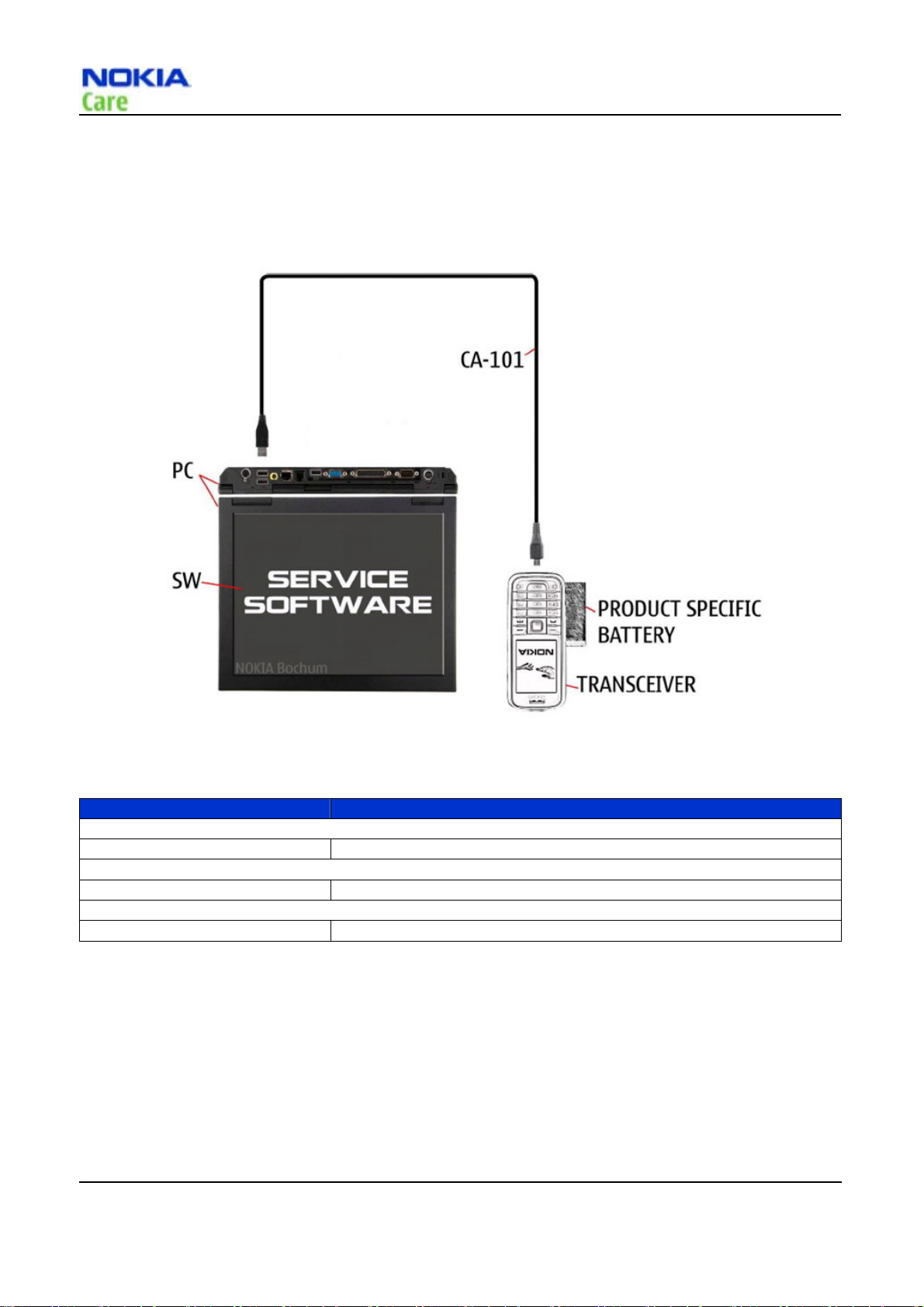
Service tools
Product Specific tools
The table below gives a short overview of service tools that can be used for testing, error analysis and repair of
product RM-376.
MJ-209 Module Jig
The module jig offers engine module component level repair and analysis.
Features:
z connection interfaces for CDMA antenna
z galvanic connection to engine module test pads
z lid interconnection with test points for measurements
z connection to Displays, earpiece, headset and speakers
Note: There is one RF connection for CDMA
Table 1 MJ-209 attenuation table
Band (mid. ch.) Channel Frequency /MHz Attenuation Loss / dB
800 TX 824 – 849 MHz
800 RX 869 – 894 MHz
Set-up Guide
1
Prepare LCM module, FPC, board and MJ-209
2
Connect LCM module and board using FPC
3
Put 2 on MJ-209
4
Close MJ-209
then start further testing
SS-190 Dome sheet Alignment Jig
SS-190 is a jig to align the adhesive dome sheet assembly onto the PWB in
the proper location during dome sheet replacement.
Issue1 Company Confidential Page 2-5
Copyright © 2009 Nokia. All rights reserved.
Page 24
RM-376
Service Tools and Service Concept
General tools
The table below gives a short overview of service tools that can be used for testing, error analysis and repair of
product RM-376
RJ-230 Soldering
RJ-230 is a jig to support component level exchange with soldering
machines for the engine module.
PK-83 AMS SW Protection Key
(USB)
PK-83 is a hardware protection key with a USB interface to enable the use
of the service software when connected to the USB port of the PC or
Notebook. It is not possible to use the service software without PK-83
Page 2-6 Company Confidential Issue1
Copyright © 2009 Nokia. All rights reserved.
Page 25
RM-376
Service Tools and Service Concept
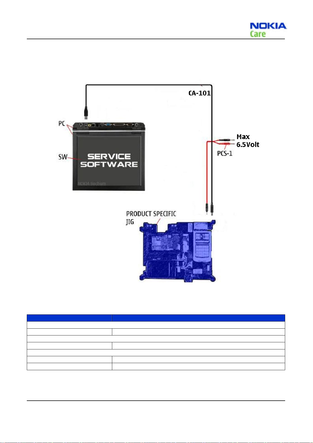
Cables
The table below gives a short overview of service tools that can be used for testing, error analysis and repair of
product RM-376.
CA-101 Micro USB cable The CA-101 is a USB-to-micro USB data cable that allows connections between the PC and the phone.
PCS-1 Power Service Cable The PCS-1 power cable (DC) is used with a docking station, a module jig or a control unit to supply a controlled voltage.
CA-128RS RF Test Cable
RF Test Cable for use with a Module Jig.
CA-128RS RF cable allow RF function tests and RF tuning in CDMA Cell
and PCS bands.
Features include:
z most accurate RF connection to phone module under test
z low attenuation and small “ripple” over the width of each band
Note: The RF Test Cable must be used for RF tuning.
SRT-6 Opening tool
SRT-6 is used to open phone covers.
Issue1 Company Confidential Page 2-7
Copyright © 2009 Nokia. All rights reserved.
Page 26
Service concepts
POS (Point of Sale) flash concept
RM-376
Service Tools and Service Concept
Figure 1 POS flash concept
Type Description
Product specific tools
BL-5BT Battery
Other tools
Nokia Care Suite PC with Nokia Care Suite service software
Cables
CA-101 Micro USB cable
Page 2-8 Company Confidential Issue1
Copyright © 2009 Nokia. All rights reserved.
Page 27
RM-376
Service Tools and Service Concept
Flash concept with Module Jig
Figure 2 Flash concept with Module Jig
Type Description
Product specific tools
MJ-209 Module Jig
Other tools
Nokia Care Suite PC with Nokia Care Suite service software
Cables
CA-101 Micro USB cable
PCS-1 Power Service Cable
Issue1 Company Confidential Page 2-9
Copyright © 2009 Nokia. All rights reserved.
Page 28
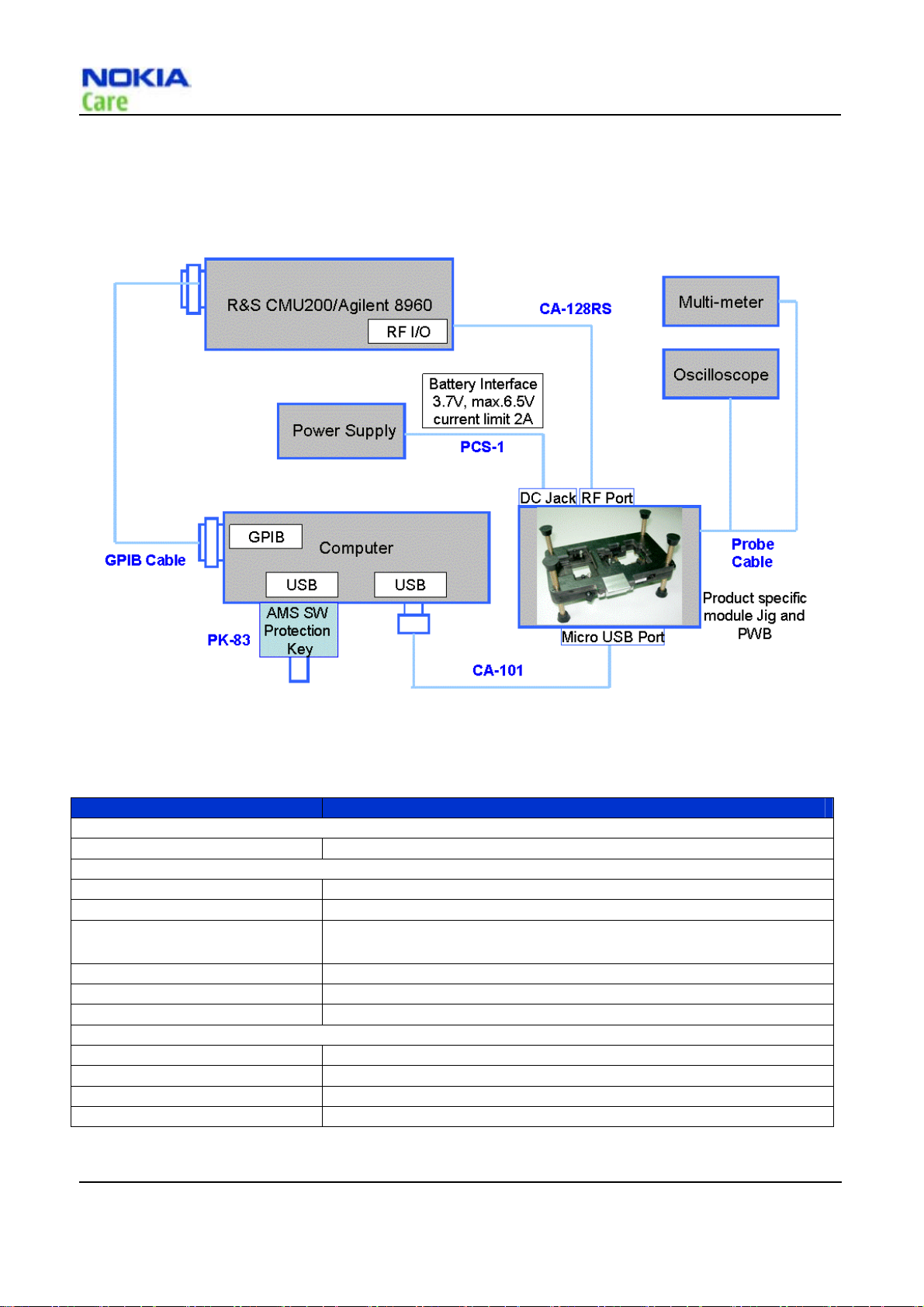
Covers-off BB/RF T roubleshooting usi ng Module Jig
RM-376
Service Tools and Service Concept
Figure 3 Cover-off BB/RF Troubleshooting using Module Jig
Type Description
Product specific tools
MJ-209 Module Jig
Other tools
PK-83 AMS SW Protection Key (USB)
Nokia Care Suite PC with Nokia Care Suite service software (L3 version)
R&S CMU200 with B89/PK800
module
Oscilloscope
Multi-meter
Probes used with Oscilloscope and Multi-meter
Cables
CA-101 Micro USB cable
PCS-1 Power Service Cable
CA-128RS RF Test Cable
GPIB Cable
CDMA CALL BOX
Page 2-10 Company Confidential Issue1
Copyright © 2009 Nokia. All rights reserved.
Page 29
RM-376
Service Tools and Service Concept
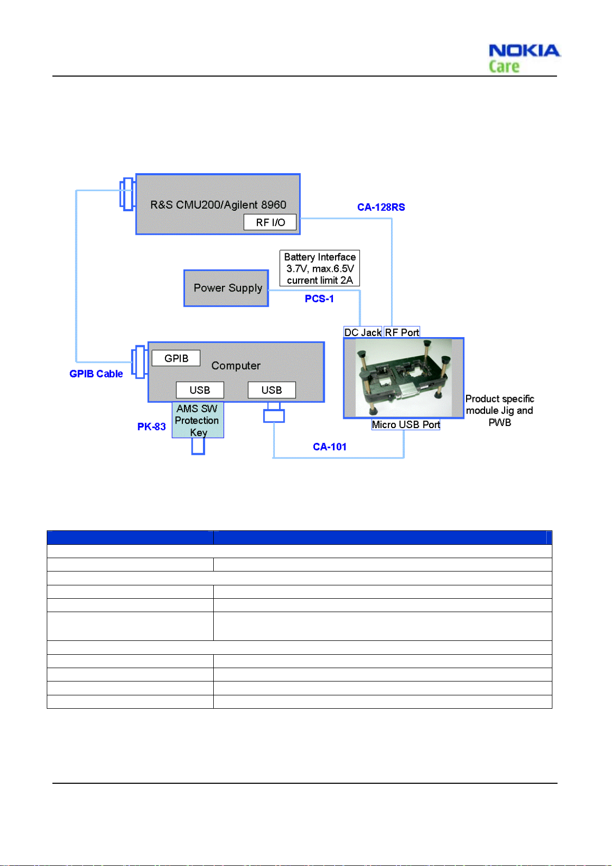
Automated T uning a nd Alignment c oncept
Figure 4 Automated Tuning and Alignment concept
Type Description
Product specific tools
MJ-209 Module Jig
Other tools
PK-83 AMS SW Protection Key (USB)
Nokia Care Suite PC with Nokia Care Suite service software (L3 version)
R&S CMU200 with B89/PK800
module
Cables
CA-101 Micro USB cable
PCS-1 Power Service Cable
CA-128RS RF Test Cable
GPIB Cable
CDMA CALL BOX
Issue1 Company Confidential Page 2-11
Copyright © 2009 Nokia. All rights reserved.
Page 30

(This page left intentionally blank.)
RM-376
Service Tools and Service Concept
Page 2-12 Company Confidential Issue1
Copyright © 2009 Nokia. All rights reserved.
Page 31

Nokia Customer Care
3- Baseband
Troubleshooting
Issue1 Company Confidential
Copyright © 2009 Nokia. All rights reserved.
Page 32

(This page left intentionally blank.)
RM-376
Baseband Troubleshooting
Company Confidential Issue1
Copyright © 2009 Nokia. All rights reserved.
Page 33

RM-376
Baseband Troubleshooting
Table of Contents
Troubleshooting overview................................................................................................................................3-3
Dead or jammed device troubleshooting .......................................................................................................3-4
General power checking..................................................................................................................................3-5
Charging troubleshooting.................................................................................................................................3-6
Keyboard troubleshooting................................................................................................................................3-7
Power key troubleshooting ..............................................................................................................................3-9
Vibra troubleshooting......................................................................................................................................3-10
Display module troubleshooting.................................................................................................................... 3-11
Audio troubleshooting.....................................................................................................................................3-12
Audio troubleshooting test instructions .........................................................................................3-12
Internal receiver troubleshooting ...................................................................................................3-17
Internal microphone troubleshooting.............................................................................................3-18
IHF speakers troubleshooting........................................................................................................3-19
External earphone troubleshooting ...............................................................................................3-20
Issue1 Company Confidential Page 3-1
Copyright © 2009 Nokia. All rights reserved.
Page 34

RM-376
Baseband Troubleshooting
Figure
Figure 1 measurement data_ receiver test................................................................................................3-13
Figure 2 measurement data_ microphone test.........................................................................................3-14
Figure 3 measurement data_ speaker test................................................................................................3-15
Figure 4 measurement data_ handset test................................................................................................3-16
Page 3-2 Company Confidential Issue1
Copyright © 2009 Nokia. All rights reserved.
Page 35

RM-376
Baseband Troubleshooting
Troubleshooting overview
For practical reasons, troubleshooting is divided into two sections;
z Baseband troubleshooting
z RF troubleshooting
Issue1 Company Confidential Page 3-3
Copyright © 2009 Nokia. All rights reserved.
Page 36

Dead or jammed device troubleshooting
Troubleshooting flow
Power on
Faults
No
Yes
· Check CN1101. Is It any SMT
Issue? If Yes ,reheat solder joints
or change a new one.
RM-376
Baseband Troubleshooting
Yes
Yes
No
No
Yes
Yes
No
No
Yes
No
Page 3-4 Company Confidential Issue1
Copyright © 2009 Nokia. All rights reserved.
Page 37

RM-376
Baseband Troubleshooting
General power checking
Check the following voltages:
Signal name Regulator Sleep Idle
VREG
2.6 V
RFRX
VREG
2.6 V
RFTX
VREG
3.3 V
USB
VREG
2.85 V
RUIM
VREG
2.85 V
TCXO
VREG
2.65 V
MSMA
VREG
1.8 V
MSME1
0 2.63 2.63 4.0
0 0 2.65 4.0
3.27 3.27 3.27 With USB Cable 4.0
2.99 2.99 3 With RUIM Card 4.0
2.89 2.89 2.87 4.0
2.67 2.67 2.68 4.0
1.83 1.83 1.81 4.0
Talk
Notes Supply
Mode
VREG
MSME2
VREG
MSMP
VREG
CORE
MIC
BIAS
2.9 V
2.6 V
1.2 V
1.8 V
2.89 2.89 2.89 4.0
2.6 2.6 2.61 4.0
1.23 1.24 1.22 4.0
0 1.83 1.84
At turning-on the audio
4.0
path
Issue1 Company Confidential Page 3-5
Copyright © 2009 Nokia. All rights reserved.
Page 38

Charging troubleshooting
Troubleshooting flow
RM-376
Baseband Troubleshooting
Page 3-6 Company Confidential Issue1
Copyright © 2009 Nokia. All rights reserved.
Page 39

RM-376
Baseband Troubleshooting
Keyboard troubleshooting
Context
There are two possible failure modes in the keyboard module:
z One or more keys can be stuck, so that the key does not react when a keydome is pressed. This kind of failure is
caused by mechanical reasons (dirt, rust)
z Malfunction of several keys at the same time; this happens when one or more rows or columns are failing
(shortcut or open connection). For a more detailed description of the keyboard and keymatrix, see section
Keyboard.
If the failure mode is not clear, start with the Keyboard Test in L3 PST.
Issue1 Company Confidential Page 3-7
Copyright © 2009 Nokia. All rights reserved.
Page 40

Troubleshooting flow
RM-376
Baseband Troubleshooting
Page 3-8 Company Confidential Issue1
Copyright © 2009 Nokia. All rights reserved.
Page 41

RM-376
Baseband Troubleshooting
Power key troubleshooting
Troubleshooting flow
Yes
No No
Yes
Yes
Issue1 Company Confidential Page 3-9
Copyright © 2009 Nokia. All rights reserved.
Page 42

Vibra troubleshooting
Troubleshooting flow
No No
RM-376
Baseband Troubleshooting
Yes
Yes
No
Yes
Page 3-10 Company Confidential Issue1
Copyright © 2009 Nokia. All rights reserved.
Page 43

RM-376
Baseband Troubleshooting
Display module troubleshooting
Troubleshooting flow
Issue1 Company Confidential Page 3-11
Copyright © 2009 Nokia. All rights reserved.
Page 44

RM-376
Baseband Troubleshooting
Audio troubleshooting
Audio troubleshooting test instructions
Single ended external earpiece and differential internal earpiece/IHF outputs can be measured either with a single
ended or a differential probe.
When measuring single ended, each output is measured against ground.
Note: Do not connect ground of single ended probe to 2nd signal of differential lines.
Internal handsfree output is measured using a current probe, if a special low-pass filter designed for measuring a
digital amplifier is not available. Note also, that when using a current probe, input signal frequency must be set to
2kHz.
The signal for input is single ended.
Required equipment
The following equipment is needed for the tests:
z Oscilloscope
z Function generator (sine waveform)
z Current probe (Internal handsfree PWM output measurement)
z service software, Nokia L3 PST Fx.xx
z Power supply 3.7V
Test procedure
Audio can be tested using MIT (*#648#). Four different audio loop paths can be activated:
• Receiver test
• Microphone test
• Speaker test
• Headset test
Correct pins an signals for each test see following table.
Audio loop tests and test results
The results presented in the table apply, when no accessory is connected. Earpiece, internal mic and speaker are
in place during measurement. Applying a headset accessory during measurement causes a significant drop in
measured levels.
Page 3-12 Company Confidential Issue1
Copyright © 2009 Nokia. All rights reserved.
Page 45

RM-376
Baseband Troubleshooting
Measurement data
Receiver test
Figure 1 measurement data_ receiver test
Issue1 Company Confidential Page 3-13
Copyright © 2009 Nokia. All rights reserved.
Page 46

Microphone test
RM-376
Baseband Troubleshooting
Figure 2 measurement data_ microphone test
Page 3-14 Company Confidential Issue1
Copyright © 2009 Nokia. All rights reserved.
Page 47

RM-376
Baseband Troubleshooting
Speaker test
Figure3 measurement data_ speaker test
Issue1 Company Confidential Page 3-15
Copyright © 2009 Nokia. All rights reserved.
Page 48

Headset test
RM-376
Baseband Troubleshooting
Figure4 measurement data_ handset test
Page 3-16 Company Confidential Issue1
Copyright © 2009 Nokia. All rights reserved.
Page 49

RM-376
Baseband Troubleshooting
Internal receiver troubleshooting
Troubleshooting flow
Issue1 Company Confidential Page 3-17
Copyright © 2009 Nokia. All rights reserved.
Page 50

Internal microphone troubleshooting
Troubleshooting flow
RM-376
Baseband Troubleshooting
Yes
Yes
No
No
Page 3-18 Company Confidential Issue1
Copyright © 2009 Nokia. All rights reserved.
Page 51

RM-376
Baseband Troubleshooting
IHF speakers troubleshooting
Troubleshooting flow
No No
Yes
No
Yes
Yes
No
Yes
Issue1 Company Confidential Page 3-19
Copyright © 2009 Nokia. All rights reserved.
Page 52

External earphone troubleshooting
Troubleshooting flow
No No
RM-376
Baseband Troubleshooting
Yes
Yes
No
Yes
Page 3-20 Company Confidential Issue1
Copyright © 2009 Nokia. All rights reserved.
Page 53

Nokia Customer Care
4- RF Troubleshooting
Issue1 Company Confidential
Copyright © 2009 Nokia. All rights reserved.
Page 54

(This page left intentionally blank.)
RM-376
RF Troubleshooting
Company Confidential Issue1
Copyright © 2009 Nokia. All rights reserved.
Page 55

RM-376
RF Troubleshooting
Table of Contents
General RF troubleshooting ............................................................................................................................4-3
Introduction to RF troubleshooting ..................................................................................................4-3
General information on RF troubleshooting ...................................................................................4-3
RF key components .........................................................................................................................4-5
General voltage checking.................................................................................................................4-6
RF CallTest in Nokia CDMA L3 PST Fx.x ....................................................................................4-10
Receiver troubleshooting ...............................................................................................................................4-12
Introduction to receiver (RX) troubleshooting...............................................................................4-12
Setup for RX Troubleshooting .......................................................................................................4-12
Cell Receiver Check from RF to DVGA .......................................................................................4-14
Receiver RF test point ....................................................................................................................4-14
CELL 800 RX Path Troubleshooting.............................................................................................4-16
Transmitter troubleshooting...........................................................................................................................4-17
Setup for TX Troubleshooting........................................................................................................4-19
Transmitter RF test point................................................................................................................4-20
CELL 800 TX Path Troubleshooting.............................................................................................4-21
FM radio troubleshooting ...............................................................................................................................4-22
RF tunings .......................................................................................................................................................4-24
Introduction to RF tunings..............................................................................................................................4-24
Autotuning ........................................................................................................................錯誤! 尚未定義書籤。
Figure
Figure 1 RF TX Path voltage checking test
points ………………………………………………………………………………4-6
Figure 2 Bottom side TX voltage checking test
point…………………………………………………………………………4-7
Figure 3 RF RX voltage checking test
point…………………………………………………………………………………………4-8
Figure 4 RF Toolkit setup for RX
troubleshooting……………………………………………………………...……………....4-12
Figure 5 RX RF test
points…………………………………………………………………………………………………………
……….4-14
Figure 6 Typical
readings………………………………………………………………………………………………………
…………..4-17
Figure 7 RF Toolkit setup for TX
troubleshooting……………………………………………………………………………...4-18
Figure 8 TX RF test
point……………………………………………………………………………………………………………
………4-19
Issue1 Company Confidential Page 4-1
Copyright © 2009 Nokia. All rights reserved.
Page 56

Figure 9 Auto tuning concept with CMU200/Agilent
8960 ………………………………………………………………4-24
RM-376
RF Troubleshooting
Page 4-2 Company Confidential Issue1
Copyright © 2009 Nokia. All rights reserved.
Page 57

RM-376
RF Troubleshooting
General RF troubleshooting
Introduction to RF troubleshooting
Most RF semiconductors are static discharge sensitive
ESD protection must be applied during repair (ground straps and ESD soldering irons).
Pre-baking
These parts are moisture sensitive and must be pre-baked prior to soldering:
z RFIC xxxx
z PA xxxx
Discrete components
In addition to the key-components, there are a number of discrete components (resistors, inductors and capacitors)
for which troubleshooting is done mainly by
Capacitors: check for short circuits.
Resistors: check value with an ohm meter.
Note: In-circuit measurements should be evaluated carefully
visual inspection.
Measuring equipment
All measurements should be done using:
z An oscilloscope for low frequency and DC measurements. Recommended probe: 10:1, 10Mohm//8pF.Title of
the Document + Issue Number/Date of publication
z A radio communication tester including RF generator and spectrum analyser, for example Rohde & Schwarz
CMU200. (Alternatively a spectrum analyser and an RF generator can be used. Some tests in this guide are not
possible to perform if this solution is chosen).
Note: All measurements with an RF coupler should be performed in an RF-shielded environment because
nearby base stations can disturb sensitive receiver measurements. If there is no possibility to use RF
shielded environment, testing at frequencies of nearby base stations should be avoided.
Level of repair
The scope of this guideline is to enable repairs at key-component level. Some key-components are not accessible,
i.e. not replaceable. Please refer to the list of Non-replaceable RF components.
General information on RF troubleshooting
The RF frontend solution has two signal paths to the antenna feed points.
Issue1 Company Confidential Page 4-3
Copyright © 2009 Nokia. All rights reserved.
Page 58

Crystal 19.2MHz
RM-376
RF Troubleshooting
FM ch ip
QSC6020 single Chip
RX SAW f i l t er
Power detector
Front-end Module RF con n ector
Antenna Pin
Page 4-4 Company Confidential Issue1
Copyright © 2009 Nokia. All rights reserved.
Page 59

RM-376
RF Troubleshooting
RF key components
Issue1 Company Confidential Page 4-5
Copyright © 2009 Nokia. All rights reserved.
Page 60

RF Troubleshooting
General voltage checking
RF TX voltage checking
Steps
1. Set up the main board in the module jig. The phone should be in local mode.
2. Check the following:
# Signal name Test point Voltage (all bands)
1 PA_ON C1801.2 On :2.35~2.85V , Off :0V
2 PA_R0 C1802.2 Low mode :2.35~2.85V , High mode :0V
3 VREG_TCXO C1809.2 On :2.85V , Off :0V
4 VPH_PWR C1807.1 3.4~4.2V
5 VREG_RFTX C814.1 2.65V
*
RM-376
Page 4-6 Company Confidential Issue1
Copyright © 2009 Nokia. All rights reserved.
Page 61

RM-376
RF Troubleshooting
Figure 1 RF TX Path voltage checking test points
Issue1 Company Confidential Page 4-7
Copyright © 2009 Nokia. All rights reserved.
Page 62

RF Troubleshooting
# Description Test Point Value RF Supply Lines Resistance to Ground
1 VREG_MSMP, C608.1 2.6V >290kΩ to ground
2 VPH_PWR,
3 VREG_MSMC,
4 VREG_MSMA,
5 VREG_TCXO,
6 VREG_RFRX,
7 VREG_RFTX,
Table 2 Bottom side TX voltage checking test points and RF Supply Line Resistance to Ground
*Note: Always measure resistance m easure resistance with the phone powered off
C514.1 3.4~4.2V >200kΩ to ground
C622.1 1.2V >18kΩ to ground
C615.1 2.6V >37kΩ to ground
C602.1 2.85V ~500kΩ to ground
C803.1 2.65V >274kΩ to ground
C808.1 2.65V ~276kΩ to ground
RM-376
1
5
3
7
6
4
2
Figure 2 Bottom side TX voltage checking test point
Page 4-8 Company Confidential Issue1
Copyright © 2009 Nokia. All rights reserved.
Page 63

RM-376
RF Troubleshooting
RF RX voltage checking
# Description Test Point Value
1 XO_19.2M X801.1, X801.3 19.2 MHz
2 VREG_RFRX C803.1 2.65V
3 Rx bias R1705.2 122mV
Figure 3 RF RX voltage checking test point
Issue1 Company Confidential Page 4-9
Copyright © 2009 Nokia. All rights reserved.
Page 64

RM-376
RF Troubleshooting
RF CallT est in Nokia CDMA L3 PST Fx.x
Context
Always start the troubleshooting procedure by running the RF CallTest in Nokia CDMA L3 PST. If a test fails,
please follow the diagram below.
If the phone is dead and you cannot perform the self tests, go to Dead or jammed device troubleshooting in the
baseband troubleshooting section.
Setup for RX T roubleshooting
Use the following steps to configure FTM mode for RF troubleshooting.
1. Connect RF connector to a spectrum
2. Put PWB on the module jig, connect data service cable between PC and Module Jig and connect a power
supply
3. Launch Nokia CDMA L3 PST Fx.x Service Software and run RF Toolkit function
4. The RF and Testing box appears
5. Select “RF and Testing “
6. Press “START” Button
Page 4-10 Company Confidential Issue1
Copyright © 2009 Nokia. All rights reserved.
Page 65

RM-376
RF Troubleshooting
Troubleshooting flow
Issue1 Company Confidential Page 4-11
Copyright © 2009 Nokia. All rights reserved.
Page 66

RM-376
RF Troubleshooting
Receiver troubleshooting
Introduction to receiver (RX) troubleshooting
RX can be tested by making a phone call or in local mode. For the local mode testing, use the RF CallTest in Nokia
CDMA L3 PST service software.
The main RX troubleshooting measurement is RSSI reading. This test measures the signal strength of the received
signal.
Setup for RX T roubleshooting
Use the following steps to configure FTM mode for RF troubleshooting.
1. Connect RF test connector to a CMU.
2. Connect mobile terminal to a PC via the Module Jig, and connect a power supply.
3. Open RF Toolkit in L3 program.
4. Set Start RF connection in “ connection ” box
5. Change to FTM in “phone mode setting” box.
6. Select a Band (Cellular) in “Band setting” box.
7. Write a channel in “RF channel setting” box.
Cellular Band Test channel : 384
< Set RF channel to 384 on CMU at the same time >
8. Select “0-LNA R0” in set LNA range box
9. Key in -92.6 in AGC box and then click “dBm to AGC” button.
< Set RF level=-92.6 dBm on CMU >
10. Click “Get DVGA “button.( DVGA value is only operated in high gain mode )
11. Select “1--LNA R1” in set LNA range box
12. Key in -81.8 in AGC box, and then click “dBm to AGC” button.
< Set RF level=-81.8 dBm on CMU >
13. Click “Get LNA offset “button.
14. Repeat 11-13 steps for getting LNA offsets of LNA2 and LNA3.
<Key in -53.8 dBm and -43.8 dBm in AGC box corresponding to LNA2 and LNA3>
After testing, it’ s necessary to change to “Online” in “Phone mode setting” box.
Page 4-12 Company Confidential Issue1
Copyright © 2009 Nokia. All rights reserved.
Page 67

RM-376
8
9 7 5
3
RF Troubleshooting
4
3
6
Figure4 RF Toolkit setup for RX troubleshooting
10
1
12
Issue1 Company Confidential Page 4-13
Copyright © 2009 Nokia. All rights reserved.
Page 68

RM-376
RF Troubleshooting
Cell Receiver Check DVGA and LNA offset value
LNA Range DVGA LNA1 LNA2 LNA3
Input RF level (dBm)
Reasonable offset value
-92.6 -81.8 -53.8 -43.8
10~70 80~152 160~277 280~430
Receiver RF test point
For the test points in below figure, an external signal source of –25 dBm was injected to the RF input. Set LNA
GAIN STATE = 0 .The signal was then traced throughout the receiver chains. A CMU200 call box is
recommended. (Open non-signaling mode, press the SG soft button, and then select CW.) Inject a continuous
wave (CW) for Cell (881.52MHz) at a fixed –25 dBm power level. Measurements were taken with the RF Probe.
Signal levels are approximate, and the accuracy may be +/- 2 dB or more depending on the probe position and
grounding.
# Test Point Description Value
1 C1806.2 RF Connector to FEM -30dBm
2 C1814.1 FEM OUTPUT -33dBm
3 L1701.1 LNA IN -30dBm
4 L1711.1 RX SAW INPUT -22dBm
5 C1711.1 RX SAW OUTPUT -23dBm
6 L1709.2, L1707.1 RX MIXER IN -27dBm
Page 4-14 Company Confidential Issue1
Copyright © 2009 Nokia. All rights reserved.
Page 69

RM-376
RF Troubleshooting
5
6
3
4 2
1
Figure 5 RX RF test points
Issue1 Company Confidential Page 4-15
Copyright © 2009 Nokia. All rights reserved.
Page 70

CELL 800 RX Path T roubleshooting
Troubleshooting flow
RX Path faults
Ge t b a d DV GA
YES
RM-376
RF Troubleshooting
Measure RX volt age.
Is it OK?
YES
Measure FEM output.
Probe RX test point 2.
YES
Measu re RX SAW INPUT
Probe RX test point 4.
No
YES
Measure RF connector
to FEM. Probe RX test
point 1.
YES
Measu re LNA I N.
Probe RX test point 3.
No
Check U100
No
Check U1801 No
No
Check C1707,
L1704, L1705,
L1711
Check C1806,
J1801
Check C1814,
L1701, L1702
YES
Measu re RX SAW
Measur e MI XER IN
Probe RX test point 6.
YES
En d
OUT PUT
Probe RX test point 5.
YES
No
YES
Get DVGA value 10~100
Check C1711,
L1710, L1700,
C1710, L1706,
L1707
No
Ch e c k U 1 7 0 1No
Go t o r el ev a n t
troubleshooting section
Page 4-16 Company Confidential Issue1
Copyright © 2009 Nokia. All rights reserved.
Page 71

RM-376
RF Troubleshooting
Note:
• QSC6020 is underfilled and can not be replaced.
• Memory IC is underfilled and can not be replaced.
• The Shielding Cover can not be reused after removal.
• After using the heatgun, the domesheet needs to be replaced.
Transmitter troubleshooting
Steps
1. Set the phone to normal mode
2. Use the following settings:
3. Check the basic TX parameters (i.e. power, phase error, modulation and switching spectrum), using a
communication analyzer (for example CMU200).
Issue1 Company Confidential Page 4-17
Copyright © 2009 Nokia. All rights reserved.
Page 72

RF Troubleshooting
Figure 6 Typical readings
4. Change the power level (RF controls) and make sure the power reading follows accordingly.
RM-376
Page 4-18 Company Confidential Issue1
Copyright © 2009 Nokia. All rights reserved.
Page 73

RM-376
RF Troubleshooting
Setup for TX T roubleshooting
Use the following steps to configure FTM mode for RF troubleshooting.
1. Connect RF connector to a spectrum
2. Put PWB on the module jig, connect data service cable between PC and Module Jig and connect a power
supply
3. Launch Nokia CDMA L3 PST Fx.x Service Software and run RF Toolkit function
4. The RF Toolkit box appears
5. Set “Start RF connection”
6. Set “Set Mode“ to “FTM”
7. Set “Set Band ” to “Cellular band 800”
8. Set “Set Channel “ to Channel “384”
9. Set “Set PA Range” to “1” --> “R0=1”
10. Set “Waveform” to “ON”
11. Set “Set TX on/off” to “ON”
12. Set “Set TX AGC” to “80”
13. Get HDET value by setting “Set ADC Channel” to “4” and “Get ADC”.
Figure 7 RF Toolkit setup for TX troubleshooting
Issue1 Company Confidential Page 4-19
Copyright © 2009 Nokia. All rights reserved.
Page 74

RF Troubleshooting
T ransmitter RF test point
# Test Point Description Value
1 L1801.1, L1802.1 U100 DA differential output -12 dBm
2 L1801.2, L1802.2,
C1803.2, C1804.2
3 C1806.2 FEM output ( PA Low Gain MODE ) 6 dBm
4 C1806.1 FEM output to RF connector ( PA Low
5 J1801 RF connector ( PA Low Gain MODE ) 13dBm
DA output to FEM input -15dBm
6dBm
Gain MODE )
RM-376
Figure 8 TX RF test point
Page 4-20 Company Confidential Issue1
Copyright © 2009 Nokia. All rights reserved.
Page 75

RM-376
RF Troubleshooting
CELL 800 TX Path T roubleshooting
Troubleshooting flow
TX Path faults
YES
Measure TX vo ltage,
En a b l e p i n .
Are t he y OK?
OK
Measure DA output to
FEM i np u t .
Probe TX test point 2.
OK
FEM o u tp u t t o RF
con nect or
Probe TX test point 4.
No
YES
Measure DA differential
output. Probe TX test
point 1.
NOK
OK
FEM o u tp u t
Probe TX test point 3.
Check U100,
L801, L802,
Check U100NOK
Check L1801,
L1802, C1803,
C1804, C1815,
C1816
Check U1801NOK
Check C1806NOK
OK
Measure RF connector
Is HDET value
resonable?
OUT PUT
Probe TX test point 5.
OK
Check U1802No
YES
En d
Check J1801NOK
Issue1 Company Confidential Page 4-21
Copyright © 2009 Nokia. All rights reserved.
Page 76

RM-376
RF Troubleshooting
FM radio troubleshooting
FM V olt age T est Point
# Test Point Description Value
1 C1602.1, C1603.1 Vph 3.4V~4.2V
2 C1604.2 Vreg_ MSMP 2.6V
Troubleshooting flow
Page 4-22 Company Confidential Issue1
Copyright © 2009 Nokia. All rights reserved.
Page 77

RM-376
RF Troubleshooting
On ly n oise i s audible?
Connect headset to
phone jack J1001 and
listen to FM signal
FM Fa u lt
YES
No
NOK
YES
Check t he solderi ng
points of C1601, B1004,
C1025, C1017, C1018 and
replace them
No FaultOK
IS FM radio function OK?OK
OK
Go to Headset
troubleshooting
NOK
Check Vph=3.4~4.2V at
C1602, C1603
OK
Check Vreg_MSMP=2.6V
at C1604
OK
Replace U1601
OK
EN D
NOK
NOK
NO
Go t o g en e r a l
power supply
troubleshooting
YES
NOK
OK
Issue1 Company Confidential Page 4-23
Copyright © 2009 Nokia. All rights reserved.
Page 78

RM-376
RF Troubleshooting
RF tunings
Introduction to RF tunings
Important: Only perform RF tunings if:
z one or more of the RF components have been replaced
z Flash memory chip is replaced or corrupted.
RF calibration is always performed with the help of a product-specific module jig, never with an RF coupler.
Using an RF coupler in the calibration phase will cause a complete mistuning of the RF part.
Important: After RF component replacements, always use autotuning. Manual tunings are only
required in rare cases.
Cable and adapter losses
RF cables and adapters have some losses. They have to be taken into account when the phone is tuned. As all RF
losses are frequency dependent, the user has to act very carefully and understand the measurement setup.
For RF attenuations of the module jig please refer to the Service tools section.
Auto tuning
This phone can be tuned automatically.
Autotune is designed to align the phone's RF part easier and faster. It performs calibrations, tunings and
measurements of RX and TX. The results are displayed and logged in a result file, if initiated.
Hardware set up
Hardware requirements for auto tuning:
z PC (Windows 2000/XP) with GPIB card
z Power supply
z Product specific module jig
z Cables: CA-128RS (RF cable), CA-101 Micro USB cable, PCS-1 Power Service Cable and GPIB cable
z PK-83 AMS SW protection key
z Service Software, Nokia CDMA L3 PST Fx.x (x.x means version number)
Page 4-24 Company Confidential Issue1
Copyright © 2009 Nokia. All rights reserved.
Page 79

RM-376
RF Troubleshooting
Figure 9 Auto tuning concept with CMU200/Agilent 8960
Service software preparations
Install the phone-specific data package. This defines the phone-specific settings.
RF cable loss setting procedure
1. Make sure the phone (in the jig) is connected to the equipment. Else, some menus will not be shown in
CDMA L3 PST Fx.x
2. Select “RF and Testing” and click “cable loss”.
3. Select Band class to BC0 for 2608.
4. If RF cable loss is kno wn, select “set ini” and enter the loss value.
5. If RF cable loss is unknown, select “calculate”.
6. In order to create a golden phone, we utilize CA-128RS as RF cable and set the loss to 0.5 dB.
7. Change RF cable (extend or replace it) and click “next” button.
8. Calculate the loss value, click “calculate” button.
Issue1 Company Confidential Page 4-25
Copyright © 2009 Nokia. All rights reserved.
Page 80

RM-376
RF Troubleshooting
Page 4-26 Company Confidential Issue1
Copyright © 2009 Nokia. All rights reserved.
Page 81

RM-376
RF Troubleshooting
Issue1 Company Confidential Page 4-27
Copyright © 2009 Nokia. All rights reserved.
Page 82

Page 83

Nokia Customer Care
5- System Module and User
Interface
Issue1 Company Confidential Page 5-1
Copyright © 2009 Nokia. All rights reserved.
Page 84

(This page left intentionally blank.)
RM-376
System Module and User Interface
Page 5-2 Company Confidential Issue1
Copyright © 2009 Nokia. All rights reserved.
Page 85

RM-376
System Module and User Interface
Table of Contents
Introduction........................................................................................................................................................5-4
Phone description .............................................................................................................................5-4
Energy management .......................................................................................................................................5-6
Battery and charging.........................................................................................................................5-6
Backup battery ..................................................................................................................................5-9
Normal and extreme voltages..........................................................................................................5-9
Power key and system power-up..................................................................................................5-10
Power off..........................................................................................................................................5-12
Modes of operation .........................................................................................................................5-13
Power distribution............................................................................................................................5-14
Clock distribution .............................................................................................................................5-16
USB ..................................................................................................................................................5-22
Charger interface ............................................................................................................................................5-22
User Interface..................................................................................................................................................5-23
Display module................................................................................................................................5-23
Keyboard and other keys...............................................................................................................5-24
Audio concept .................................................................................................................................................5-26
Audio HW architecture ...................................................................................................................5-26
Internal microphone ........................................................................................................................5-27
Internal earpiece..............................................................................................................................5-27
Internal speaker...............................................................................................................................5-28
Vibra circuitry ...................................................................................................................................5-28
AV Connector ..................................................................................................................................5-29
Baseband technical specifications................................................................................................................5-30
External interfaces ..........................................................................................................................5-30
Charger connector and charging interface connections & electrical characteristics................5-30
RF Description ................................................................................................................................................5-31
Block diagram..................................................................................................................................5-31
Receiver (RX)..................................................................................................................................5-31
Transmitter (TX) ..............................................................................................................................5-32
Frequency mappings .....................................................................................................................................5-35
CDMA 800 frequencies ..................................................................................................................5-35
Issue1 Company Confidential Page 5-3
Copyright © 2009 Nokia. All rights reserved.
Page 86

RM-376
System Module and User Interface
Introduction
Phone description
The mobile terminal using a CDMA single mode engine (Cellular/ 800) with Qualcomm baseband consists of the
following ASICs:
z Qualcomm Single Chip 6020, including RF transmitter and receiver, Baseband and Power management
these three categories
z 32Mb Flash memory with 16Mb Psram memory
The QSC60X0 device represents QCT’s next generation of chipset architecture and enhancements for voice and
entry-level multimedia handsets. The QSC60X0 device integrates the Mobile Station Modem™ (MSM™)
baseband, radioOne RF, and power management functionality into a single 15 × 15 mm mini scale package
(MSP). These functions perform all of the signal processing and power management tasks within a mobile device.
This architecture reduces handset complexity, cost, time to market, and board-space requirements while
providing many of the most popular features and functions.
3G products based on the QSC60X0 device may include:
z Voice centric phones
z Music player enabled devices and applications
z Camera phones (requires the QSC6030 device)
z Entry level multimedia phones
z Other applications and devices
QSC60X0-based products benefit from enhanced security, text, graphic and picture messaging, high quality
audio and speakerphone support, polyphonic ringtones, voice capture, MP3/AAC/AAC+ music playback,
megapixel image capture, and other applications using the core Wireless Internet Lauchpad features.
The QSC60X0 solution also provides a seamless migration path from 2G to 3G services and applications,
including the 4GV™ vocoder for increased voice capacity for CDMA2000® 1X networks. It is designed to exceed
the specifications of mobile devices for worldwide cdmaOne™ and 3G 1xMC systems, including those based
upon the IS-95A/B and IS-2000 standards.
The QSC60x0 device extends the level of integration to include radio frequency and power management
functions.
BL-5BT (870 mAh) lithium-ion battery is used as the main power source.
Key components
Function Description Item ref
Main chip Qualcomm QSC6020 U100
PA
Oscillators
Memory S71WS128PC0HF3SR0 U901
Battery BL-5BT
Battery connector CN501
RF connector
Charging IC BQ24072 U503
Page 5-4 Company Confidential Issue1
Copyright © 2009 Nokia. All rights reserved.
Page 87

RM-376
System Module and User Interface
System module block diagram
Issue1 Company Confidential Page 5-5
Copyright © 2009 Nokia. All rights reserved.
Page 88

Board and module connections
RM-376
System Module and User Interface
Energy management
Battery and charging
BL-5BT battery
The 2608 uses a Lithium-Ion cell battery with a capacity of 870 mAh. QSC6020 reads the resistor inside the battery
pack on the BSI line to identify the battery size. Different charging algorithm will be used for different battery sizes.
The resistors are connected to the BSI pin inside the battery connector.
Figure 1 BL-5BT battery pack pin order
Page 5-6 Company Confidential Issue1
Copyright © 2009 Nokia. All rights reserved.
Page 89

RM-376
System Module and User Interface
Battery connector
The battery connector is a blade connector. It has three blades;
z BSI (Battery size indicator)
z GND (Ground)
z VBAT (Battery voltage)
The BSI line is used to recognize the battery capacity by a battery internal pull down resistor.
Figure 2 Battery Connector
Charging
This phone is charged through the Micro USB interface with the AC-6U travel charger.
Figure 3 AC-6U travel charger
The PM charge control is dependent on the charger type and the battery size. External components are needed
for electromagnetic compatibility (EMC), and transient protection of the input to the baseband module. The
charger’s DC input is through the Micro USB connector. This mobile terminal supports AC-6U & DC-6 chargers.
Issue1 Company Confidential Page 5-7
Copyright © 2009 Nokia. All rights reserved.
Page 90

RM-376
System Module and User Interface
Figure 4 Simplied power flow diagram
Charger Detection
Connecting a charger creates a voltage on the DC_PWR of the Charging IC. Charging starts when the PM detects
the DC_PWR input voltage level between 4.35V~6.6V and /PGOOD pin pulls to GND (/PGOOD is pin 7of
charging IC). The charger detected when CHG_DEC_N_GPIO_53 pulls low (GND).
The battery is charged in three phases: conditioning, constant current , and constant voltage. In all charge phases,
an internal control loop monitors the IC junction temperature and reduces the charge current if the internal
temperature threshold is exceeded.
The charger power stage and charge current sense functions are fully integrated. The charger function has high
accuracy current and voltage regulation loops, charge status display, and charge termination. The input current
limit and charge current are programmable using external resistors.
GPIO_55
CBL_PWR_N
VBAT
BATID/T
GND
MGND
MGND
0
1
0
1
Charge Current (mA)
100mA (USB Mode)
500mA (USB Mode)
545mA (Wall Mode)
200uA (Standby)
CHG_EN1_GPIO_55
CHG_EN2_GPIO_54
TP503
C503
0.1uF/16 V
0402C
USB_ID
USB_DP
USB_DM
USB_VBUS
4
5
DC_PWR
R519
TBD
R-0201
R502 0R R-0201
R505 TBD 0402R
R511 3K(1%) 0402R
R512 680(1%) 0402R
R513 TBD 0402R
R514 10K R-0201
USB_ID
USB_DP
USB_DM
VCOIN
C504
1uF/10V
0402C
VPH_PWR
VBAT
C502
1uF/35V
0603C
AB16
AB17
AA17
AA15
AA16
W18
W15
W16
V15
V16
W17
13
6
5
4
15
12
16
14
1
U503
BQ24072
PQFP-N16
USB_ID
USB_DP
USB_DM
USB_VBUS
VCOIN
CHG_CNT_N
VCHG
ISNS_P
ISNS_M
VBAT
BAT_FET_N
U100-5
QSC6020
QSC6020
OUT
OUT
BAT
BAT
CHG
VSS
VSS
VDD_IN_C ORE
VPH_PWR
10
11
+
C513
15uF/10V
CASE_M_S
VBAT
2
3
CHG_PGOOD _N
7
9
17
8
AA18
VDD_I N
V14
VDD_I N
T19
VDD_I N
W14
VDD_I N
W21
VDD_I N
N15
VDD_I N
P18
VDD_I N
U19
VDD_I N
AB14
VPH_PWR
C505
0.1uF/16 V
0402C
C514
4.7uF/10 V
0603C
VREG_MSMP_2.6V
R506
TBD
0402R
VPH_PWR
C506
0.1uF/16 V
0402C
C515
1000pF/16V
C-0201
R507
100K
R-0201
C507
0.1uF/1 6V
0402C
CHG_ON_N_GPIO_56
VPH_PWR
C508
0.1uF/16V
0402C
IN
EN1
EN2
CE
TD
PGOOD
ILIM
ISET
TMR
TS
CHARGER
GPIO_54
6
5
4
C501
1uF/10V
0402C
BATT_ID
R501
TBD
R-0201
DC_PWR
0
0
1
1
R503
680K
R-0201
R504
220K
R-0201
USB_VBUS
Cable_Plug
CN501
3
2
1
BATCON-FOXLINK
CN5-BT-P3_7
USB_PWR
VBAT
R515
680K
0402R
VBAT
C509
R516
1uF/10V
1M
0402C
0402R
BATT_THERM
TP501
BATT_ID
TP502
VBAT
C518
C517
1uF/10V
0402C
100pF/50V
C-0201
F501
FUSE(1A 0603)
0603R
5
SENSE
4
VDD
U504
TPS3803-01
PDSO-G5
BATT_THERM
12
R517
1M
0402R
RESET
GND
GND
T501
PESD5V0S1BL
SOD882
DC_PWR
D501
2A/30V DIODE SC HOTTKY
SOD323F
3
CHG_DEC_N_GPIO_53
1
2
VREG_MSMA_2.6V
BATT_THERM
VREG_MSMA_2.6V
BATT_ID
VBAT
R518
100K
R-0201
R508
68K(1%)
0402R
R510
68Kohm(1%,NTC)
0402R
R509
100K
0402R
C519
100pF/50V
C-0201
CHG_PGOOD_N
1
2
Q501
NTUD3128NT5G
SOT-963-6P
1
.
T502
.
90pF/5.5V
0402C
2
S1
G1
D23S2
D1
G2
VPH_PWR
Figure 5 Mobile terminal charger circuit
Page 5-8 Company Confidential Issue1
Copyright © 2009 Nokia. All rights reserved.
Page 91

RM-376
System Module and User Interface
Charger Control
In active mode, charging is controlled by charging IC. Charging voltage and current monitoring are used to limit
charging into a safe area.
Cut Off MaxCurrent = 1.5A
MaxVoltage= 6.6V
Backup battery
When the main battery is not attached EM ASIC (N2200) goes in backup mode using back-up battery that supplies
voltage to RTC in EM ASIC (N2200).
Normal and extreme voltages
Energy management is mainly carried out in the two Application Specific Integrated Circuits (ASICs) BETTY and
AVILMA. These two circuits contain a number of regulators. In addition there are some external regulators too.
In the table below, normal and extreme voltages are shown when a BL-5BT battery is used.
Voltage Voltage [V] Condition
General Conditions
Nominal voltage 3.7
Lower extreme voltage 3.145
Higher extreme voltage 4.230
(fast charging) 4.230
HW Shutdown Voltages
Vmstr+ 2.1 ± 0.1 Off to on
Vmstr+ 2.1 ± 0.1 Off to on
SW Shutdown Voltages
Sw shutdown 3.20 In call
Sw shutdown 3.20 In idle
Min Operating Voltage
Vcoff+ 2.9 ± 0.1 Off to on
Vcoff- 2.6 ± 0.1 On to off
Issue1 Company Confidential Page 5-9
Copyright © 2009 Nokia. All rights reserved.
Page 92

RM-376
System Module and User Interface
Power key and system power-up
The QSC6020 controls the power up and reset. The baseband can power up in the following ways:
z Pressing the Power button, which means to ground the KPD_PWR_N (“KPD_PWR_N” pin in 2608
schematic) pin of the QSC6020
z Connecting the charger to the charger input.
After receiving one of the above signals, the PM will start to enter reset mode. The watchdog starts, and if the
battery voltage is greater than its threshold (3V), a 6ms delay starts to allow MSM to settle. After this delay elapses,
the VERG_MSMC regulator enables. Then, VERG_MSMP, VERG_MSMA & VERG_TCXO regulators are
enabled in sequence after MSMC. There is a 120us (4 Sleep_Clocks) delays between each regulator’s turn on.
The PON_RESET_N (“RESIN_N” pin in 2608 schematic) line holds low for another 20ms and is sent to MSM.
Resets are generated for the MSM’s internal MCU and its internal DSP, and MSM sends TCXO_ON
(“TCXO_EN” pin in 2608 schematic) signal to PM to enable TCXO. After PON_RESET_N goes high, MSM holds
PS_HOLD at low state for 200ms and then drives PS_HOLD to high state. This will keep all regulators at on
state in order to complete this power on sequence. KPD_PWR_N key can be released after PS_HOLD goes
high.
The RESOUT_N from QSC6020 is used to reset flash memory during power up and to put the flash memory in
power down during sleep mode. LCD_RS from QSC6020 is used to reset LCD module during power up. All
baseband regulators are switched on when the PM is powered on. The QSC6020s internal watchdog runs and
resets during normal operation. If the watchdog expires, it will generate a reset signal to reset to MSM status.
Then, QSC6020 drives RESOUT_N and LCD_RS low to reset flash memory and LCD module. Below figure
represents the PM start-up sequence from reset to power-on.
Figure 6 Power-on/Power-off sequence and timing
The mobile terminal can use the power key or a charger to power up.
Page 5-10 Company Confidential Issue1
Copyright © 2009 Nokia. All rights reserved.
Page 93

RM-376
System Module and User Interface
Power Key
When the power key is pressed, the PM enters the power-up sequence. Pressing the power key causes the
KPD_PWR_N (KPD_PWR_N pin in 2608 schematic) pin to GND. The KPD_PWR_N signal is not part of the
keypad matrix. The power key is only connected to the PM. This means that when the power key is pressed, an
interrupt will be generated to the MSM in order to power on the MCU. The MCU reads the QSC6020’s interrupt
register and notifies that it is a KPD_PWR_N interrupt. The MCU reads the status of the KPD_PWR_N signal
using the control bus. If the KPD_PWR_N signal stays low for a certain time, the MCU accepts this as a valid
power-on state and continues with the software baseband initialization. If the power key does not indicate a valid
power-on situation, the MCU powers off the baseband.
Charger
Charging is controlled by start-up charging circuitry in order to detect and start charging in cases the main battery
is empty and the PM has no supply.
Issue1 Company Confidential Page 5-11
Copyright © 2009 Nokia. All rights reserved.
Page 94

RM-376
System Module and User Interface
External Supply Source is detected
Power off
While the PS_HOLD signal from the MSM is high, and the PM is in one of its power-on states. Under this
condition, the PM continually monitors three events that could trigger a power-off sequence:
z The MSM drives the PS_HOLD signal low responding to the pressing of the keypad power button
z Battery voltage drops below power off threshold (Battery voltage < 3.2 V)
z The PM die temperature exceeds its “severe” over-temperature threshold
Page 5-12 Company Confidential Issue1
Copyright © 2009 Nokia. All rights reserved.
Page 95

RM-376
System Module and User Interface
Modes of operation
Mode Description
Power-off In power-off mode, power (VPH_PWR) is supplied to the PM, RF PA,
vibrator, and keypad backlight LED. During this mode, the current
consumption is approximately 8.8 uA
Sleep The mobile terminal enters sleep mode only when MSM makes the
request to PM through the SBI bus. PM then enters Power Saving Mode,
and the VREG_MSMC VREG_MSMP regulators remain in power-on
stage. The 32.768 kHz crystal is enabled. TCXO buffers are off. All other
functions and regulators are controlled individually via SBI and are typically
disabled for minimum power dissipation.
It exits the Sleep mode either by the expiration of a sleep clock counter in
the PM or by some external interrupt (generated by a charger connection,
key press, headset connection, etc.). The TCXO is shut down in sleep
mode and the 32.768 kHz sleep clock oscillator is used as a reference
clock for the baseband.
Active In active mode, the mobile terminal operates normally. It scans channels,
listens to a base station, transmits and processes information. There are
several sub-states under the active mode. Depending on the mobile
terminal’s current state, there are states such as burst reception, burst
transmission, etc.
In active mode, this is a normal operating mode for PM. VREG_MSMC,
VREG_MSMP, VREG_MSMA, VREG_RUIM, VREG_RFRX,
VREG_RFTX, and VREG_TCXO regulators are all turned on. TCXO
oscillator is enabled, and TCXO buffers are turned on. All other functions
and regulators are controlled individually via SBI.
Charging Charging mode can function in parallel with any other operating mode. A
BSI resistor inside the battery pack indicates the battery type/ size. The
resistor value corresponds to a specific battery capacity. The PM
measures the battery voltage, temperature, size, and charging current.
Charger control block inside the PM controls the charging current
delivered from the charger to the battery and mobile terminal. The
maximum battery voltage is limited by turning the PM switch off when the
battery voltage reaches 4.2 V. The charging current is monitored by
measuring the voltage drop across a 0.1 ohm resistor.
Issue1 Company Confidential Page 5-13
Copyright © 2009 Nokia. All rights reserved.
Page 96

RM-376
System Module and User Interface
Power distribution
In normal operation, the baseband is powered by the mobile terminal‘s battery pack. The battery pack consists of
one lithium-ion cell with a capacity of 870 mAh and safety and protection circuits.
The PM controls the power distribution to the whole mobile terminal, which includes the baseband and the RF
regulators, but excludes the RF power amplifier (RF PA) RF power amplifier drains power from the battery directly.
The battery provides power directly to the following parts of the system:
z PM
z RF PA
z Vibrator
z Keyboard , Electric torch light& LCD backlights
The heart of the power distribution is the power control block inside the PM. It includes all the voltage regulators
and feeds the power to the entire system. The PM handles hardware power-up functions so that the regulators
are not powered on and the power up reset (PURX) is not released if the battery voltage is less than 3 V.
The baseband is powered by the following PM regulators:
Table 1 Baseband Regulators
Regulator Rating Current Voltage Notes
MSMC 300 mA 1.3 V Always enabled except during power-off mode
MSMA 150 mA 2.60 V
Enabled only when the system is powered on (Off during sleep
and power-off modes)
MSMP 300 mA 2.60 V Always enabled except during power-off mode
RUIM 150 mA 2.85 V Enabled only when RUIM card is used
TCXO 50 mA 2.85 V
Enabled only when the system is powered on (Off during sleep
and power-off modes)
Note: All output regulators voltage accuracy +/-2%
Below table includes the PM regulators for the RF.
Table 2 RF Regulators
Regulator Rating Current Voltage Notes
RFRX1 150 mA 2.60 V Enabled when the receiver is on
RFRX2 150 mA 2.60 V Enabled when the receiver is on
RFTX 150 mA 2.60 V Enabled when the transmitter is on
Note: All output regulators voltage accuracy +/-2%
Page 5-14 Company Confidential Issue1
Copyright © 2009 Nokia. All rights reserved.
Page 97

RM-376
System Module and User Interface
USB
or
Wall charger
VPH_PWR
Charging Block
Figure 7 Power Distribution
Issue1 Company Confidential Page 5-15
Copyright © 2009 Nokia. All rights reserved.
Page 98

RM-376
System Module and User Interface
Clock distribution
The QSC6020 derives its internal clock from two clock inputs, TCXO and SLEEP_CLK.
The main clock signal for the baseband generates from TCXO (Temperature-compensated crystal oscillator). The
QSC6020’s TCXO clock input supports the frequency 19.2 MHz +/-2ppm. The SLEEP_CLK provides a 32.768
kHz +/-20ppm clock source to drive the MSM controller into sleep mode. At this mode, most of the MSM is
powered down and the TCXO is disabled.
System Clocks
The power management circuits include several clock circuits whose outputs are used for general housekeeping
functions and elsewhere within the handset system. These circuits include the 19.2 MHz TCXO source, controller,
and buffers; RC oscillator; 32 kHz crystal oscillator; SLEEP clock; and SMPS clock. The baseline configurations
are shown in Figure 47, but some circuits offer multiple implementation options. Detailed descriptions of all these
functions and their options (where applicable) are presented in the following subsections.
Figure 8 TCXO and SLEEP_XTAL Block Diagram
Page 5-16 Company Confidential Issue1
Copyright © 2009 Nokia. All rights reserved.
Page 99

RM-376
System Module and User Interface
TCXO
The MSM device integrates a phase-locked loop from the TCXO clock input.
The PM optimizes TCXO operation that enables and disables appropriate circuits in the proper sequence. The
controller is enabled by the signal from the MSM. When the selected transition occurs at TCXO_EN, the
controller quickly enables the TCXO regulator and the input buffer, and begins counting SLEEP_CLK pulses.
Within an initial power on period, the TCXO will be stabilized to its own calibrated frequency. This initial period, in
units of 32.768 kHz clock pulses, is programmed into a timer within the controller. When the timer expires, the
output buffer is enabled. It synchronizes with the TCXO input such that the TCXO_OUT signal is glitch free, only
valid TCXO pulses are output.
Figure 9 TCXO Enable Timing Diagram
The input buffer (TCXO_IN) accepts sinusoidal or square wave signals at or near 19.2 MHz. The input buffer
(TCXO_IN) is powered from the TCXO regulator while the output buffer is powered by VREG_MSMP.
The regulator of TCXO is turned off after the TCXO_EN signal is removed. Upon power-up, the PM defaults to
this SBI-controlled mode with the TCXO defaulted on. This assures the MSM will always have a clock available
immediately at power-up even if TCXO_EN is low.
Issue1 Company Confidential Page 5-17
Copyright © 2009 Nokia. All rights reserved.
Page 100

TCXO waveform (19.2MHz+/-2ppm)
RM-376
System Module and User Interface
Figure 10 TCXO Timing at 25P0PC
Page 5-18 Company Confidential Issue1
Copyright © 2009 Nokia. All rights reserved.
 Loading...