

Page 1
RM-340; RM-341
Baseband Troubleshooting Instructions
General baseband troubleshooting
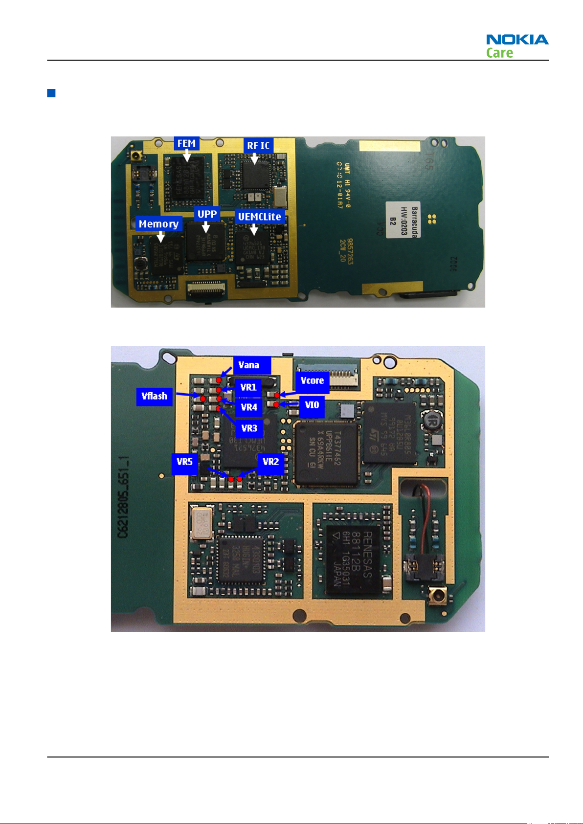
Key components
Power supply test points
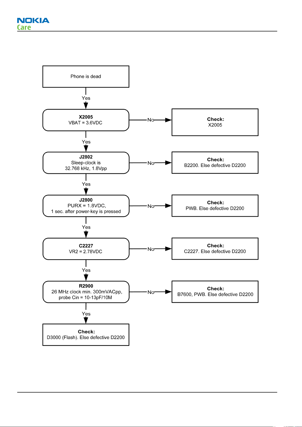
Phone cannot be powered on (I)
Context
This means that the phone does not use any current at all when the supply is connected and/or power key
is pressed. It is assumed that the voltage supplied is 3.6VDC. The UEMCLite will prevent any functionality at
battery/supply levels below 2.9VDC.
Issue 1 COMPANY CONFIDENTIAL Page 3 –5
Copyright © 2007 Nokia. All rights reserved.
Page 2
Troubleshooting flow
RM-340; RM-341
Baseband Troubleshooting Instructions
Figure 9 Troubleshooting when phone cannot be powered on
Page 3 –6 COMPANY CONFIDENTIAL Issue 1
Copyright © 2007 Nokia. All rights reserved.
Page 3
RM-340; RM-341
Baseband Troubleshooting Instructions
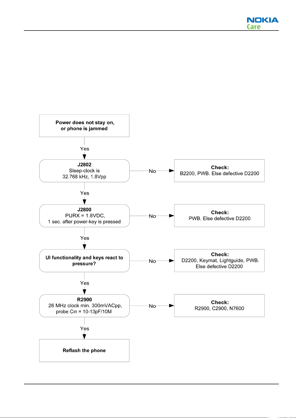
Phone cannot be powered on (II)
Context
If this kind of failure is presenting itself immediately after FLALI, it is most likely caused by ASIC's missing
contact with PWB.
If the MCU doesn’t service the watchdog register within the UEMCLite, the operations watchdog will run out
after approximately 32 seconds. Unfortunately, the service routine can not be measured.
Troubleshooting flow
Figure 10 Troubleshooting when phone does not stay on or phone is jammed
Issue 1 COMPANY CONFIDENTIAL Page 3 –7
Copyright © 2007 Nokia. All rights reserved.
Page 4

RM-340; RM-341
Baseband Troubleshooting Instructions
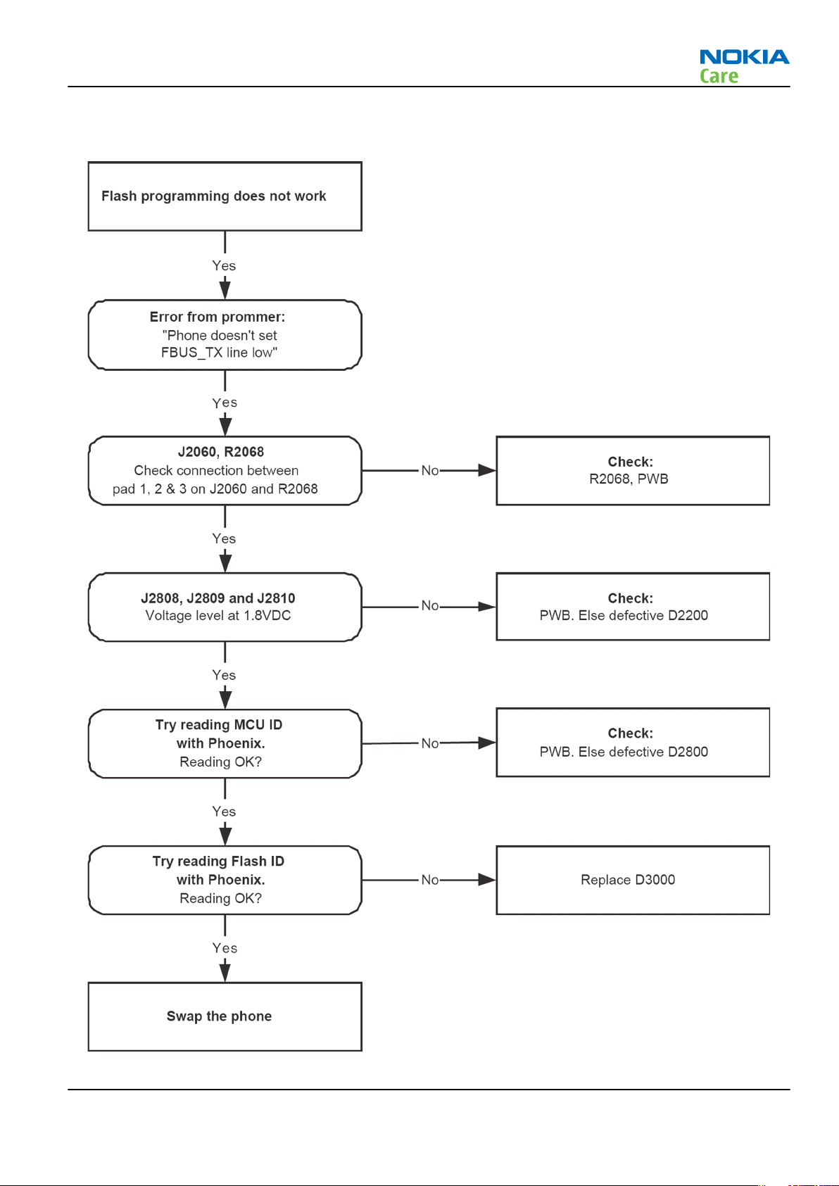
Phone cannot be flashed
Context
The flash programming can be done via the pads on the PWB (J2060). If failed, then follow up the trouble
shooting flow chart.
In case of flash failure in the FLALI station, swap the phone and send it back to the care program for further
analysis. Possible failures could be short-circuit of balls under µBGAs (UEMCLite, UPP4M, FLASH), or missing
or misaligned components.
In flash programming error cases, the flash prommer can give some information about a fault. The fault
information messages could be:
Phone doesn't set FBUS_TX line low
Because of the use of uBGA components, it is not possible to verify if there is a short circuit in the control and
address lines of MCU (UPP8M) and the memory (flash).
Page 3 –8 COMPANY CONFIDENTIAL Issue 1
Copyright © 2007 Nokia. All rights reserved.
Page 5
RM-340; RM-341
Baseband Troubleshooting Instructions
Troubleshooting flow
Figure 11 Flash programming fault
Issue 1 COMPANY CONFIDENTIAL Page 3 –9
Copyright © 2007 Nokia. All rights reserved.
Page 6

RM-340; RM-341
Baseband Troubleshooting Instructions
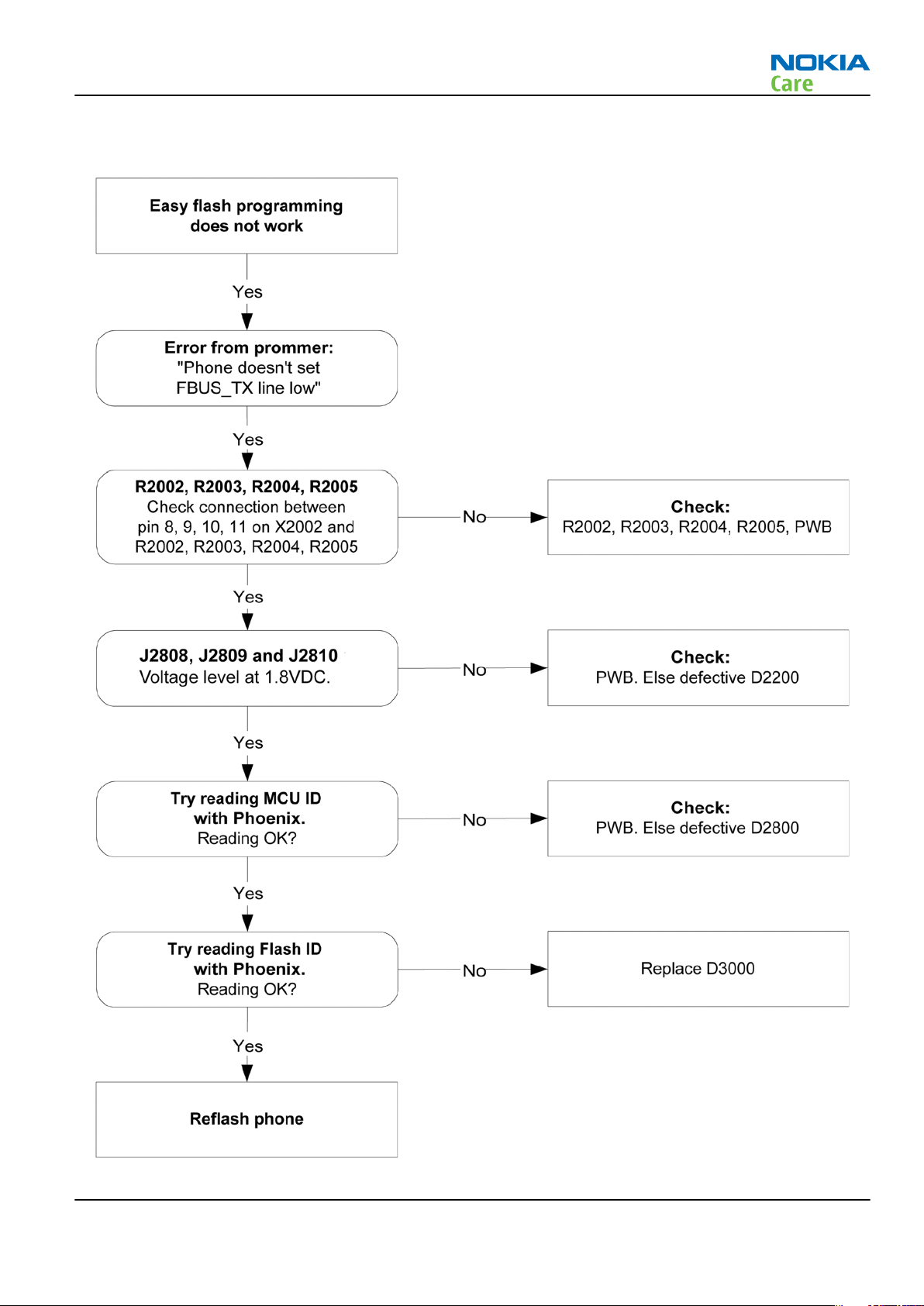
Easy flash programming does not work
Context
The flash programming can be done via the easy flash connector. If failed, then follow up the trouble shooting
below.
It is not possible to verify if there is a short circuit in control and address lines of MCU (UPP8M) and memory
(flash) because BGA package is used in RM-340/341.
Page 3 –10 COMPANY CONFIDENTIAL Issue 1
Copyright © 2007 Nokia. All rights reserved.
Page 7
RM-340; RM-341
Baseband Troubleshooting Instructions
Troubleshooting flow
Figure 12 Easy flash programming fault
Issue 1 COMPANY CONFIDENTIAL Page 3 –11
Copyright © 2007 Nokia. All rights reserved.
Page 8
RM-340; RM-341
Baseband Troubleshooting Instructions
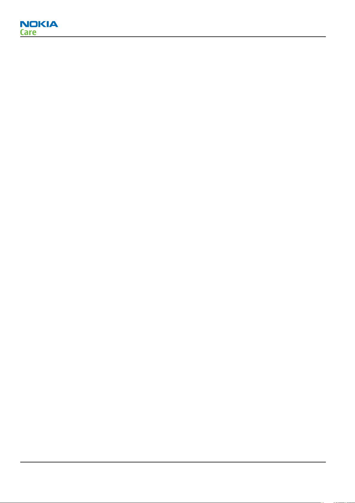
Display shows "Contact Service"
Troubleshooting flow
This error can only happen at power up where several self-tests are run. If any of these test cases fails the
display will show the message: "Contact Service".
They are individual test cases, so the below lineup of error hunting's has no chronological order. Use common
sense and experience to decide which test case to start error hunting at.
Page 3 –12 COMPANY CONFIDENTIAL Issue 1
Copyright © 2007 Nokia. All rights reserved.
Page 9
RM-340; RM-341
Baseband Troubleshooting Instructions
Figure 13 Troubleshooting when the "Contact Service" message is seen
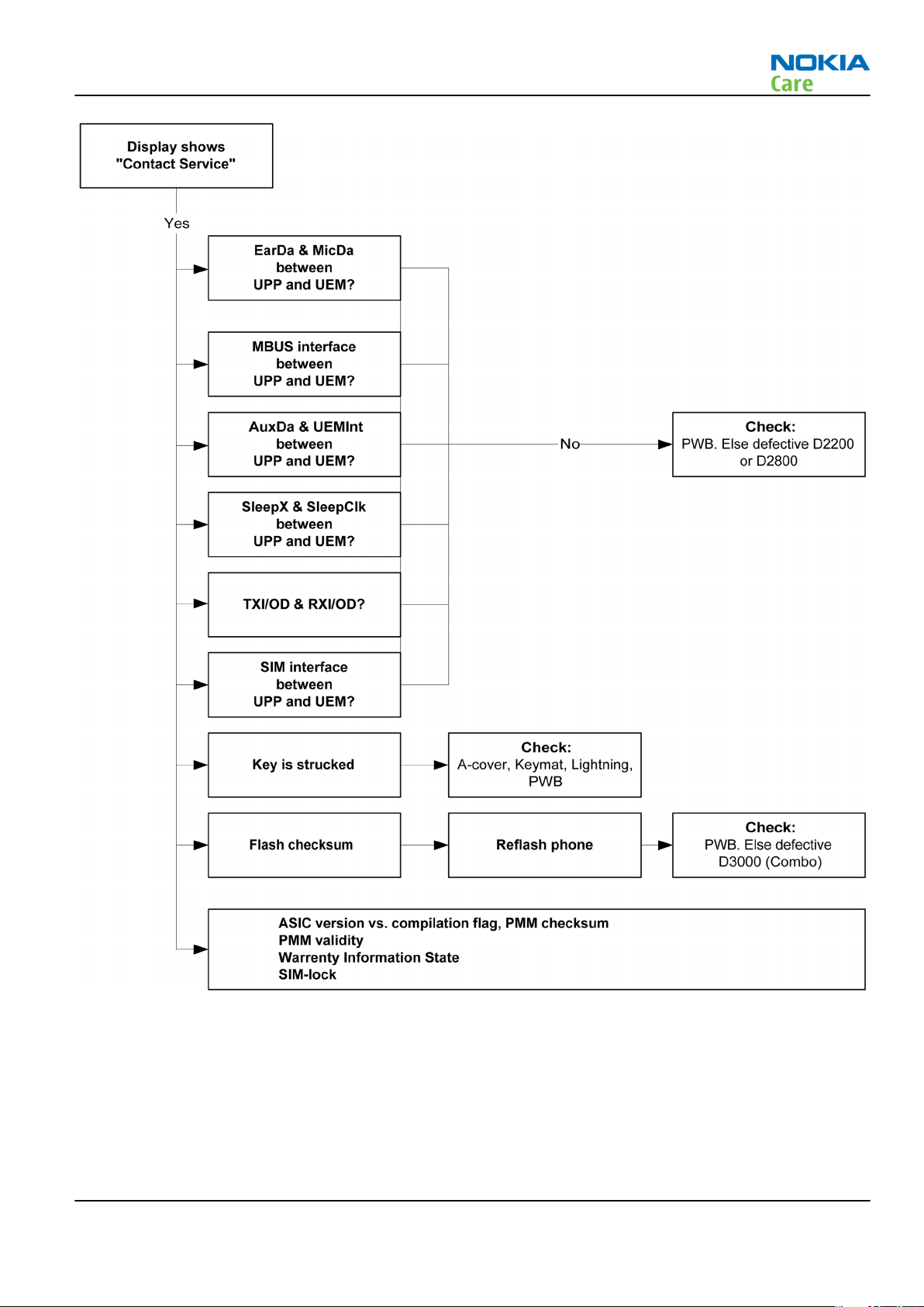
The phone does not register to the networks, or the phone cannot make a call
Context
If the phone doesn't register to the network, the fault can be in either BB or RF. Only few signals can be tested
since several signals are 'buried' in one or more of the inner layers of the PWB.
First, check that SIM LOCK is not causing the error by using a Test-SIM card and connect the phone to a tester.
Issue 1 COMPANY CONFIDENTIAL Page 3 –13
Copyright © 2007 Nokia. All rights reserved.
Page 10
Troubleshooting flow
RM-340; RM-341
Baseband Troubleshooting Instructions
Figure 14 No registering or call
Page 3 –14 COMPANY CONFIDENTIAL Issue 1
Copyright © 2007 Nokia. All rights reserved.
Page 11
RM-340; RM-341
Baseband Troubleshooting Instructions
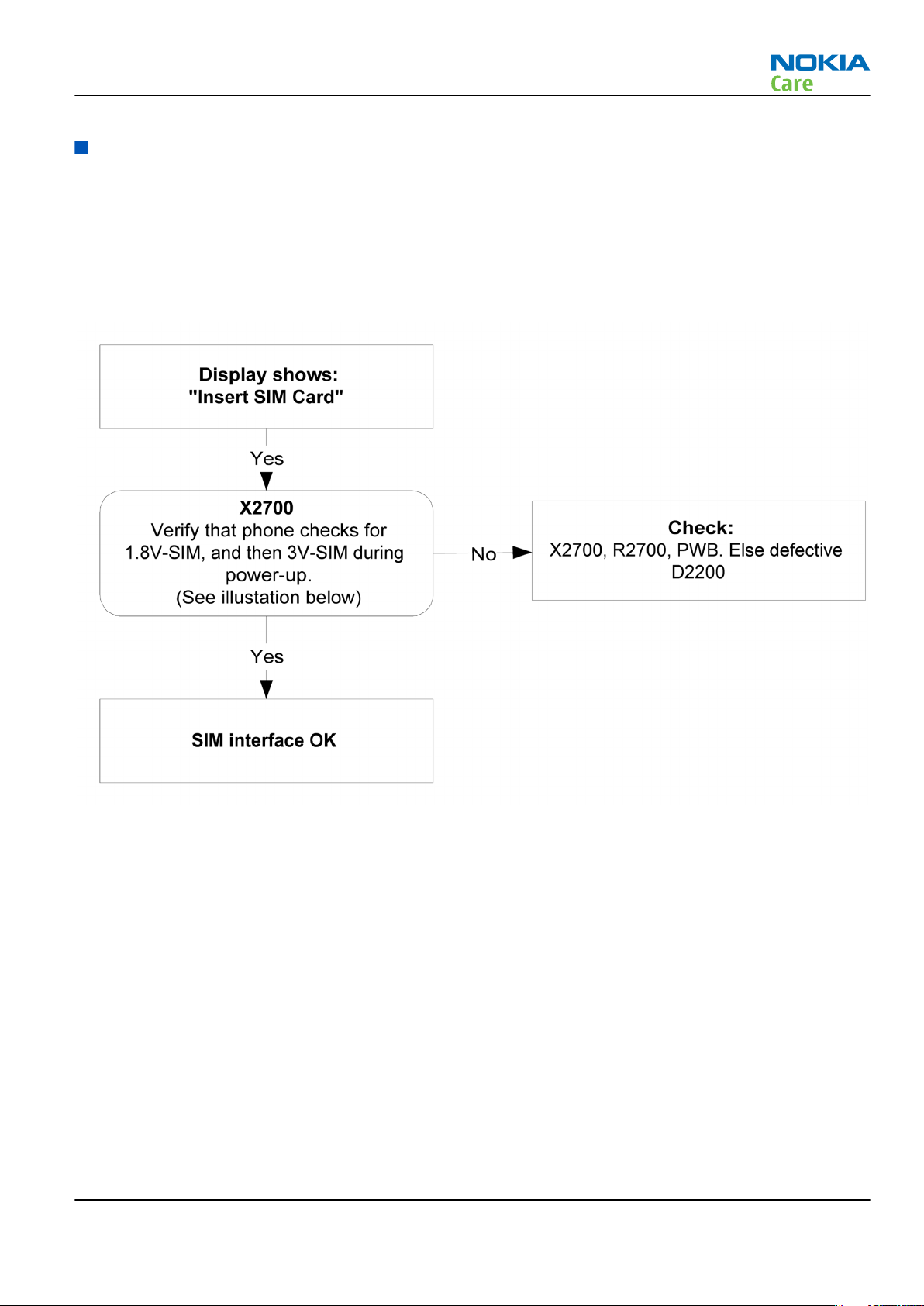
SIM related faults
Insert SIM card fault
Troubleshooting flow
The hardware of the SIM interface from UEMCLite (D2200) to the SIM connector (X2700) can be tested without
a SIM card. When the power is switched on the phone first check for a 1.8V SIM card and then a 3V SIM card.
The phone will try this four times, where after it will display ”Insert SIM card”.
Figure 15 Insert SIM card fault
Issue 1 COMPANY CONFIDENTIAL Page 3 –15
Copyright © 2007 Nokia. All rights reserved.
Page 12
RM-340; RM-341
Baseband Troubleshooting Instructions
Figure 16 Signal diagram
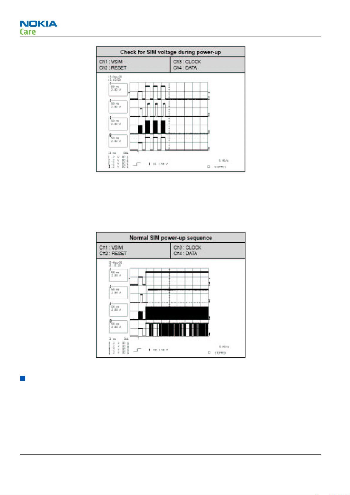
SIM card rejected
The error ”SIM card rejected” means that the ATR message received from SIM card is corrupted, e.g. data
signal levels are wrong. The first data is always ATR and it is sent from card to phone.
For reference a picture with normal SIM power-up is shown below.
Figure 17 Signal diagram
User interface
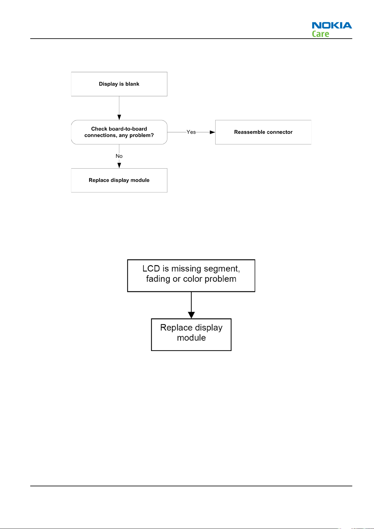
Blank display
Context
The display does not show any information at all. If there is only main or sub display blank, the problem
mostly exists in individual display. Replace related display first. For main and sub display blank, refer to
troubleshooting flow below.
Page 3 –16 COMPANY CONFIDENTIAL Issue 1
Copyright © 2007 Nokia. All rights reserved.
Page 13
RM-340; RM-341
Baseband Troubleshooting Instructions
Troubleshooting flow
Corrupted display
Context
The display contains missing or fading segments, or color presentation is incorrect.
Troubleshooting flow
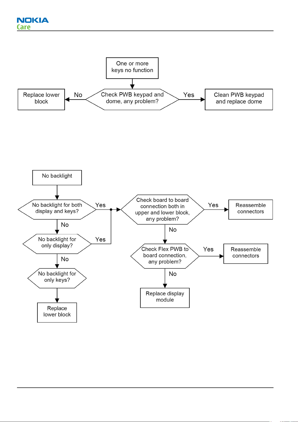
Dead keys
Context
One or more keys has no function.
Issue 1 COMPANY CONFIDENTIAL Page 3 –17
Copyright © 2007 Nokia. All rights reserved.
Page 14
RM-340; RM-341
Baseband Troubleshooting Instructions
Troubleshooting flow
No backlight for display or/and keys
Context
There are 3 kinds of statuses: No backlight for both display and keys; No backlight for only display; No
backlight for only keys.
Troubleshooting flow
Page 3 –18 COMPANY CONFIDENTIAL Issue 1
Copyright © 2007 Nokia. All rights reserved.
Page 15
RM-340; RM-341
Baseband Troubleshooting Instructions
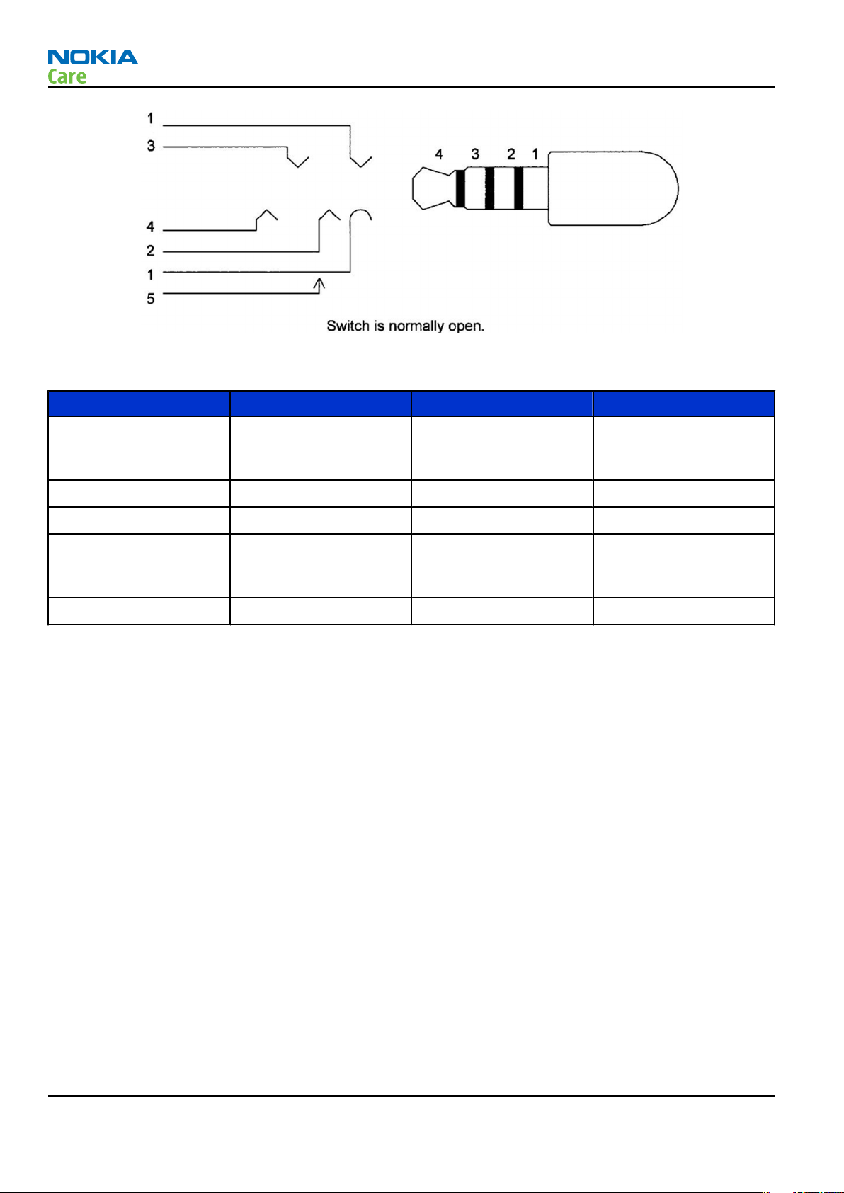
Figure 19 4-pole jack plug for audio accessory
Table 4 Connector for External Audio Accessories
Pin Signal name Direction Description
5 PLUGDET Input Terminal internal
connection, plug
detection
4 HS EAR L Output Audio output
3 HS EAR R Output Audio output
2 HS MIC Input Multiplexed
microphone audio and
control data
1 HS GND - Ground contact
Check microphone using "Hp microphone in Ext speaker out" loop
Steps
1. Connect phone with Phoenix.
2. Open “audio test” window from “Testing -> Audio test”, as shown in
above.
3. Select “Hp microphone in Ext speaker out”
4. Select "Acc. Detection" as "Off".
5. Select “Loop” as “On”
6. Input sound at microphone port, for example 94dB SPL 1kHz.
Figure Phoenix audio test window
Page 3 –20 COMPANY CONFIDENTIAL Issue 1
Copyright © 2007 Nokia. All rights reserved.
Page 16
RM-340; RM-341
Baseband Troubleshooting Instructions
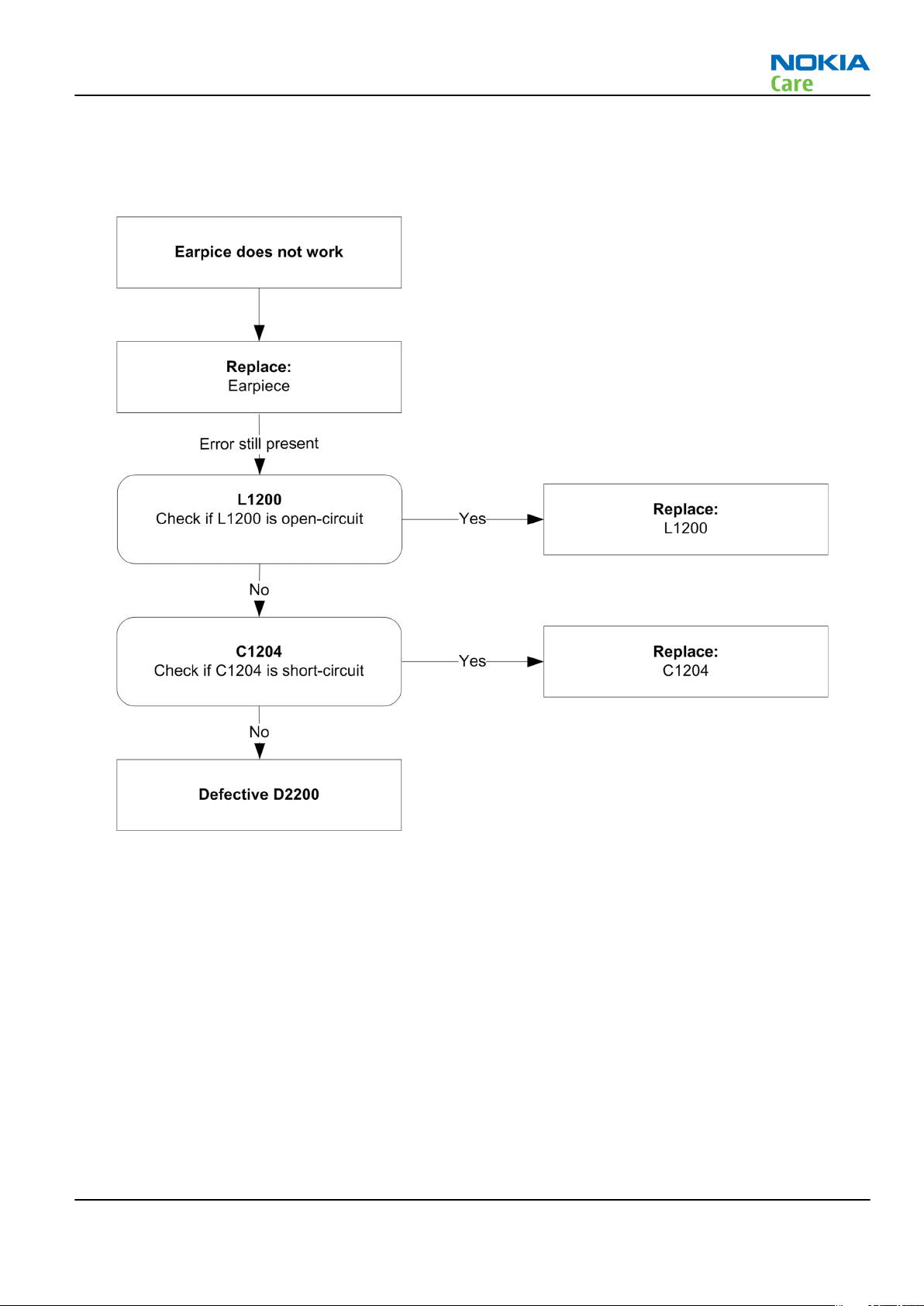
Earpiece fault
Troubleshooting flow
Figure 24 Earpiece fault flow chart
Issue 1 COMPANY CONFIDENTIAL Page 3 –23
Copyright © 2007 Nokia. All rights reserved.
Page 17
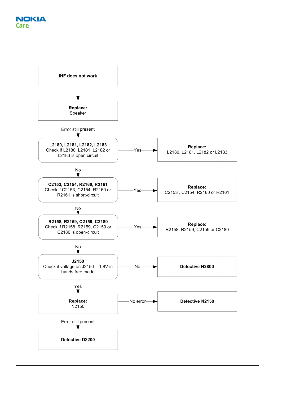
IHF/ringing tone fault
Troubleshooting flow
RM-340; RM-341
Baseband Troubleshooting Instructions
Figure 25 IHF/ringing tone fault flow chart
Page 3 –24 COMPANY CONFIDENTIAL Issue 1
Copyright © 2007 Nokia. All rights reserved.
Page 18
RM-340; RM-341
Baseband Troubleshooting Instructions
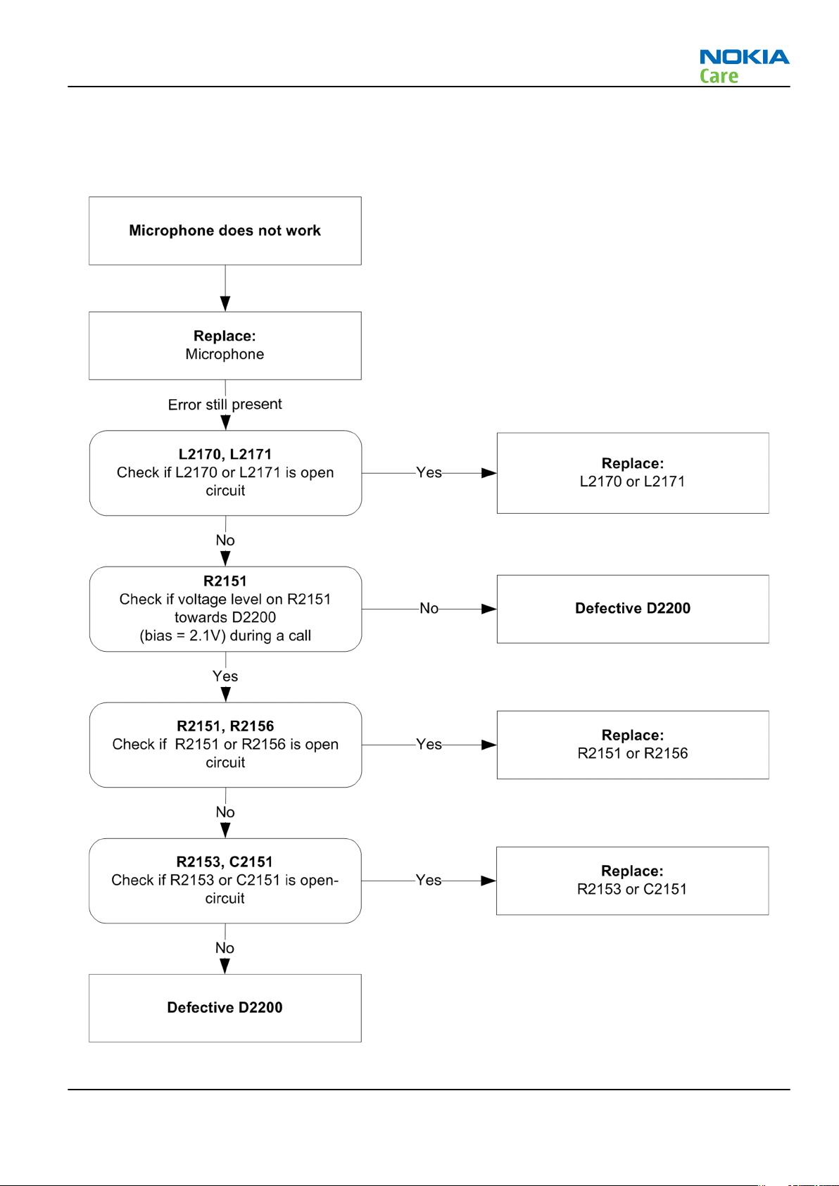
Microphone fault
Troubleshooting flow
Figure 26 Microphone fault flow chart
Issue 1 COMPANY CONFIDENTIAL Page 3 –25
Copyright © 2007 Nokia. All rights reserved.
Page 19
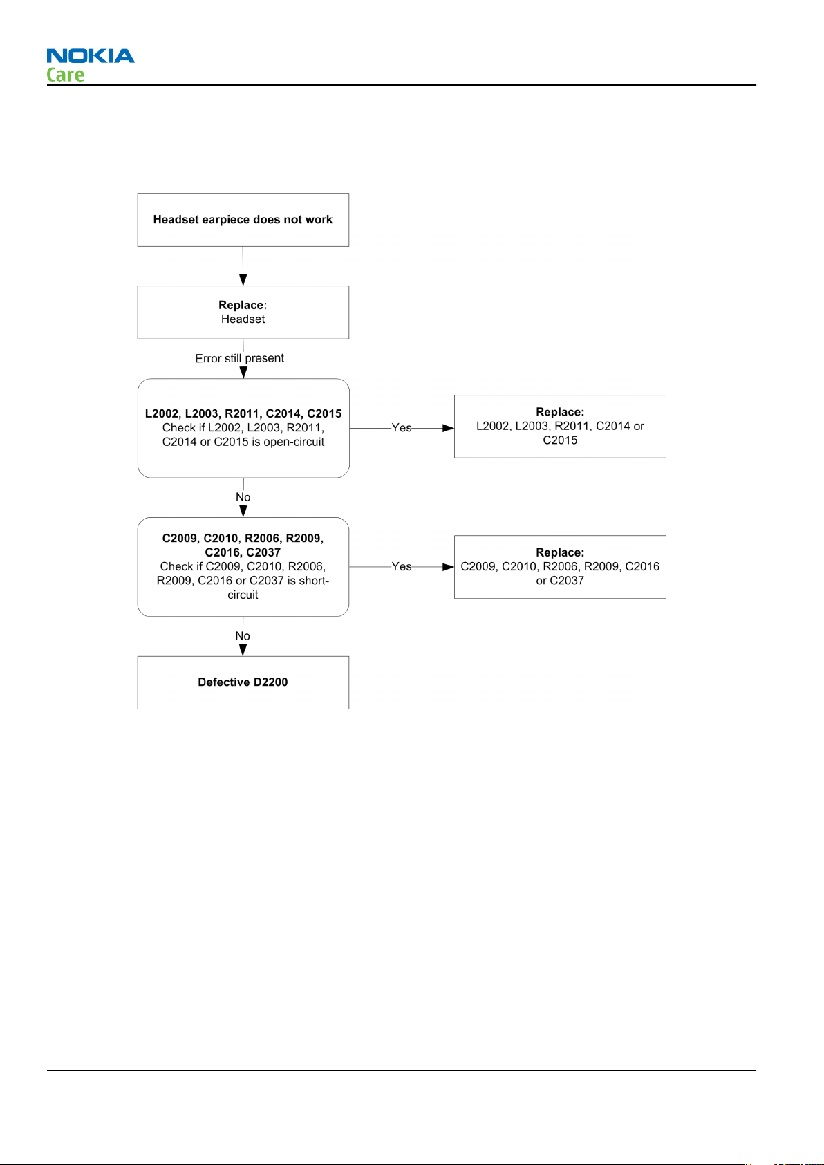
Headset earpiece fault
Troubleshooting flow
RM-340; RM-341
Baseband Troubleshooting Instructions
Figure 27 Headset earpiece fault flow chart
Page 3 –26 COMPANY CONFIDENTIAL Issue 1
Copyright © 2007 Nokia. All rights reserved.
Page 20
RM-340; RM-341
Baseband Troubleshooting Instructions
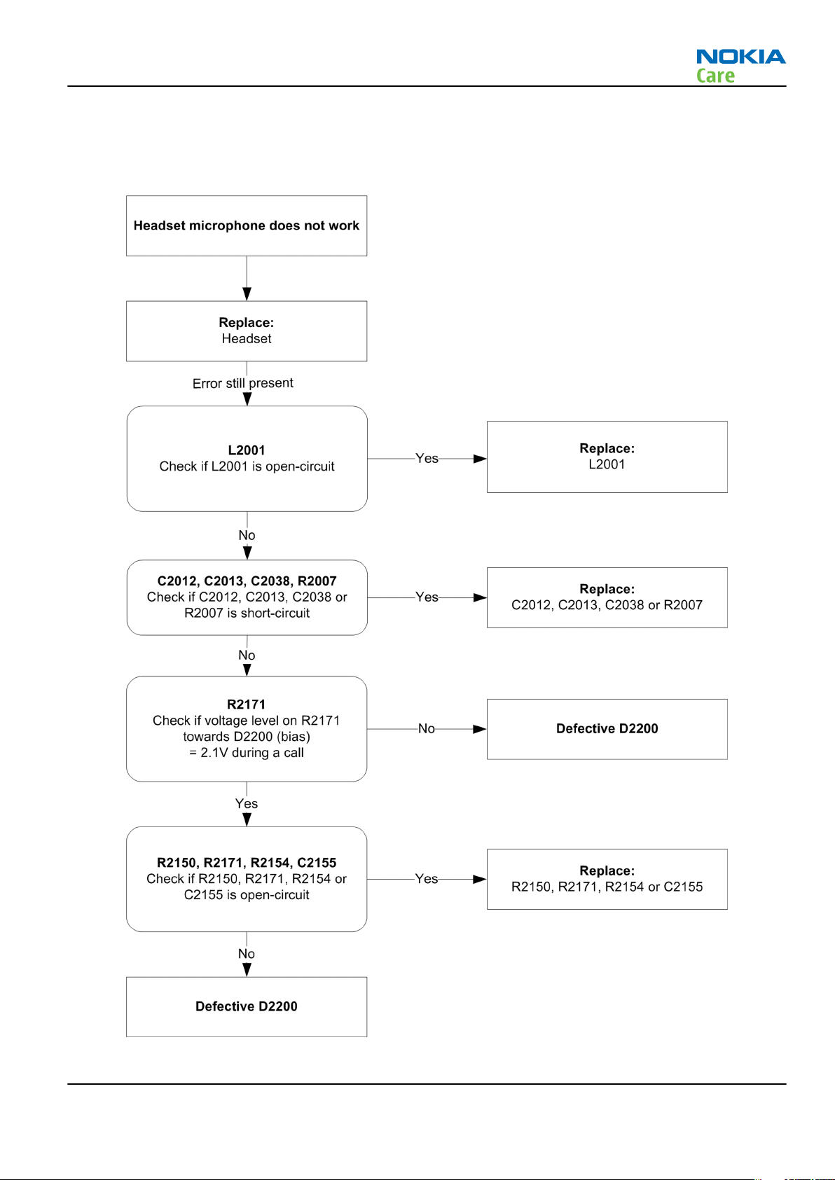
Headset microphone fault
Troubleshooting flow
Figure 28 Headset microphone fault flow chart
Issue 1 COMPANY CONFIDENTIAL Page 3 –27
Copyright © 2007 Nokia. All rights reserved.
Page 21
RM-340; RM-341
RF Troubleshooting Instructions
General RF troubleshooting
General RF troubleshooting
Most RF semiconductors are static discharge sensitive
Two types of measurements are used in the following. It will be specified if the measurement type is "RF" or
"LF".
• RF measurements are done with a Spectrum Analyzer and a high-frequency 500 ohm passive probe, for
example HP54006A. (Note that when measuring with the 500ohm probe the signal will be around 20dB
attenuated. The values in the following will have these 20dB subtracted and represent the real value seen
on the spectrum analyzer). Note that the testing have some losses which must be taken into consideration
when calibrating the test system.
• LF (Low frequency) and DC measurements should be done with a 10:1 probe and an oscilloscope. The probe
used in the following is 10Mohm/8pF passive probe. If using another probe then bear in mind that the
voltages displayed may be slightly different. Always make sure the measurement set-up is calibrated when
measuring RF parameters on the antenna pad. Remember to include the loss in the module repair jig when
realigning the phone.
So ESD protection must be applied during repair (ground straps and ESD soldering irons). Mjoelner and Bifrost
are moisture sensitive so parts must be pre-baked prior to soldering. Apart from key-components described
in this document there are a lot of discrete components (resistors, inductors and capacitors) for which
troubleshooting is done by checking if soldering of the component is done properly and checking if the
component is missing from PWB. Capacitors can be checked for short-circuiting and resistors for value by
means of an ohmmeter, but be aware in-circuit measurements should be evaluated carefully. In the following
both the name EGSM and GSM850 will be used for the lower band and both PCN and GSM1900 will be used
for the upper band.
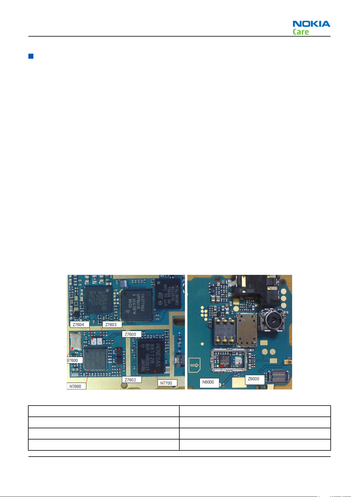
RF key components
Figure 29 RF key components on PWB
N7600 PMB3258 RF IC
N7700 FEM (PA and antenna switch)
Z7602 EGSM 850/900 RX SAW filter
Z7600 DCS 1800/PCS1900 RX SAW filter
Issue 1 COMPANY CONFIDENTIAL Page 4 –7
Copyright © 2007 Nokia. All rights reserved.
Page 22
RF Troubleshooting Instructions
Z7603 EGSM 850/900 TX filter
Z7604 DCS 1800/PCS1900 TX filter
B7600 26 MHz crystal
N6000 BT & FM IC
Z6000 BT SAW filter
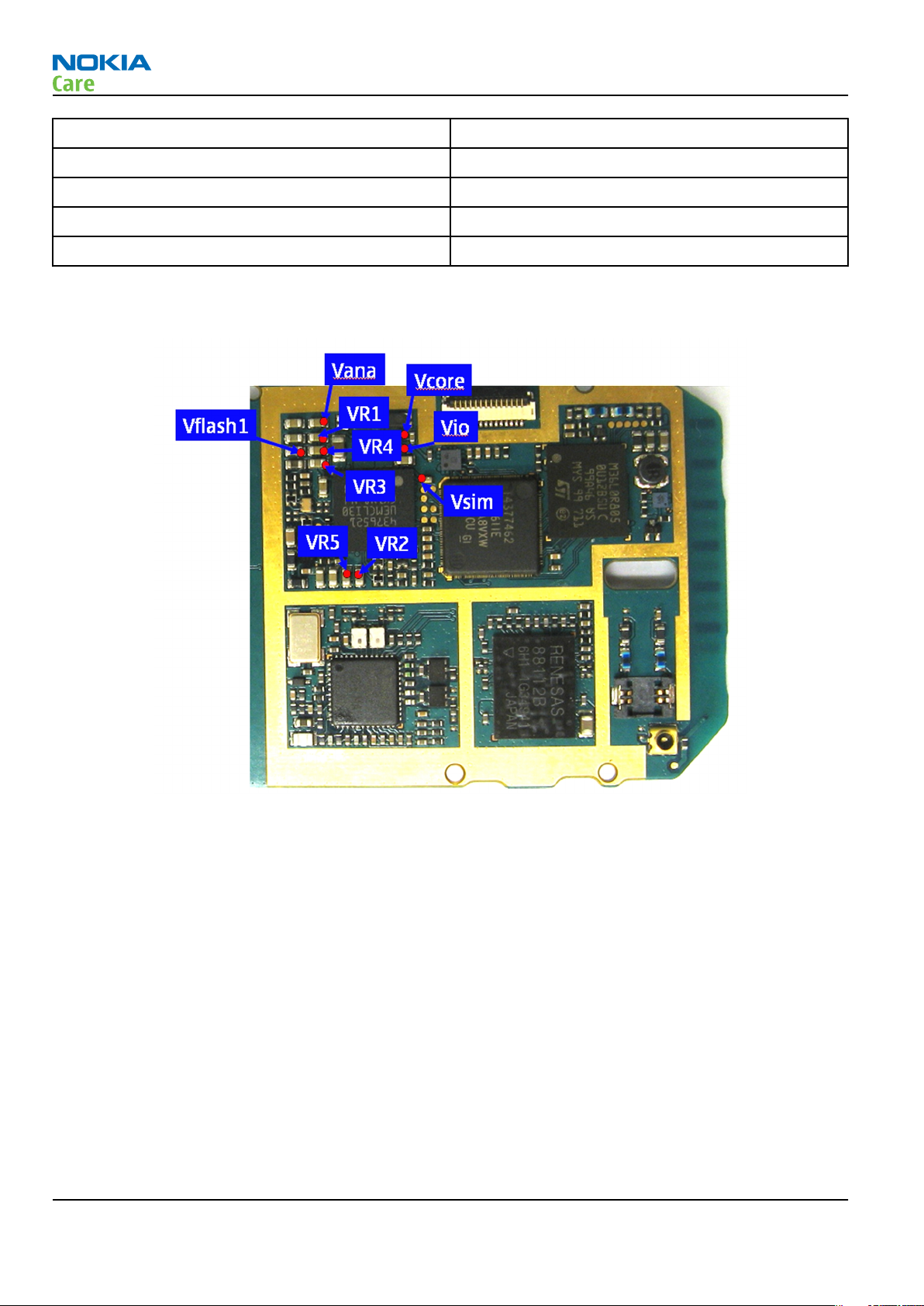
Refer to the picture below for measuring points at the UEM (D2200).
RM-340; RM-341
Figure 30 Supply points at UEM (D2200)
Page 4 –8 COMPANY CONFIDENTIAL Issue 1
Copyright © 2007 Nokia. All rights reserved.
Page 23

RM-340; RM-341
RF Troubleshooting Instructions
Figure 31 Supply point at RF IC (N7600)
Figure 32 Supply point at BT & FM IC (N6000)
Auto tuning
This phone can be tuned automatically.
Issue 1 COMPANY CONFIDENTIAL Page 4 –9
Copyright © 2007 Nokia. All rights reserved.
Page 24

RM-340; RM-341
RF Troubleshooting Instructions
Autotune is designed to align the phone's RF part easier and faster. It performs calibrations, tunings and
measurements of RX and TX. The results are displayed and logged in a result file, if initiated.
Hardware set up
Hardware requirements for auto tuning:
• PC (Windows 2000/NT) with GPIB card
• Power supply
• Product specific module jig
• Cables: 3 (alt.1) RF cable, 1 GPIB cable and DAU-9S
• Signal analyser (TX), signal generator (RX) and RF-splitter or one device including all.
Phoenix preparations
Copy the two phone specific ini-files, for example
specific folder, for example
\Phoenix\products\RM-13\
rm_13_tunings.ini
.
and
autotune_RM-13.ini,
to a phone
Auto tuning procedure
1 Make sure the phone (in the jig) is connected to the equipment. Else, some menus will not be shown in
Phoenix.
2 The first time you are using automatic tuning on this phone model, on this computer, you will have to
Set loss
3 To go to autotune, select
4 If you need more assistance, please refer to the Phoenix
for cables and jigs.
Tuning (Alt-U)
>
Auto-Tune (Alt-A)
from the menu.
Help
.
RM-340 receiver
General instructions for GSM900 RX troubleshooting
Steps
1. Connect the phone to a PC with the module repair jig.
2. Start
3. Select File and Scan product.
4. Wait a while for the PC to read the information from the phone.
5. Select Testing and RF Controls.
6. Set the parameters as follows:
Phoenix
i Active Unit: RX
ii Band: GSM 900
iii Operation Mode: Continuous mode
iv RX/TX Channel 37
v AGC: 8: FEG_ON + DTOS_ON+BB_6=Vgain_36
and establish a connection to the phone with the data cable e.g. FBUS.
Results
The setup should now look like this:
Page 4 –10 COMPANY CONFIDENTIAL Issue 1
Copyright © 2007 Nokia. All rights reserved.
Page 25

Troubleshooting diagram for GSM900 receiver
Troubleshooting flow
RM-340; RM-341
RF Troubleshooting Instructions
Figure 34 GSM900 receiver troubleshooting
Results
By measuring with an oscilloscope at RXIP or RXQP on a working GSM900 receiver this picture should be seen.
Signal amplitude peak-peak 108mV. DC offset 1.0V.
Page 4 –12 COMPANY CONFIDENTIAL Issue 1
Copyright © 2007 Nokia. All rights reserved.
Page 26

RM-340; RM-341
RF Troubleshooting Instructions
Figure 35 900 RX I/Q signal waveform
General instructions for GSM 1800 RX troubleshooting
Steps
1. Connect the phone to a PC with the module repair jig.
2. Start
3. Select File and Scan product.
4. Wait a while for the PC to read the information from the phone.
5. Select Testing and RF Controls.
6. Set the parameters as follows:
Phoenix
i Active Unit: RX
ii Band: GSM 1800
iii Operation Mode: Continuous mode
iv RX/TX Channel 700
v AGC: 8: FEG_ON + DTOS_ON+BB_6=Vgain_36
and establish a connection to the phone with the data cable e.g. FBUS.
Results
The setup should now look like this:
Issue 1 COMPANY CONFIDENTIAL Page 4 –13
Copyright © 2007 Nokia. All rights reserved.
Page 27

RM-340; RM-341
RF Troubleshooting Instructions
Troubleshooting diagram for GSM1800 receiver
Troubleshooting flow
Figure 37 GSM1800 receiver troubleshooting
Results
By measuring with an oscilloscope at RXIP or RXQP on a working GSM1800 receiver this picture should be
seen. Signal amplitude peak-peak 114mV. DC offset 1.0V.
Issue 1 COMPANY CONFIDENTIAL Page 4 –15
Copyright © 2007 Nokia. All rights reserved.
Page 28

RM-340; RM-341
RF Troubleshooting Instructions
Figure 38 1800 RX I/Q signal waveform
Measurement points in the receiver
Figure 39 RX measurements point of the control voltages to FEM N7700
Page 4 –16 COMPANY CONFIDENTIAL Issue 1
Copyright © 2007 Nokia. All rights reserved.
Page 29

RM-340; RM-341
RF Troubleshooting Instructions
Figure 40 Measurement points at the RX SAW Filters – Z7600/Z7602
Figure 41 RX I/Q signals
RM-340 transmitter
General instructions for GSM 900 TX troubleshooting
Steps
1. Apply a RF-cable to the RF-connector to allow the transmitted signal act as normal. RF-cable should be
connected to an attenuator at least 10dB before connected to the measurement equipment, otherwise
the PA may be damaged.
2. Start
3. Select File and Scan product.
4. Wait a while for the PC to read the information from the phone.
5. Select Testing and RF Controls.
6. Set the parameters as follows:
Issue 1 COMPANY CONFIDENTIAL Page 4 –17
Phoenix
i Band: GSM 900
and establish a connection to the phone with the data cable e.g. FBUS.
Copyright © 2007 Nokia. All rights reserved.
Page 30

RM-340; RM-341
RF Troubleshooting Instructions
Troubleshooting diagram for GSM900 transmitter
Troubleshooting flow
Figure 43 GSM900 tarnsmitter troubleshooting
GSM900 TX output power
Measure the output power of the phone; it should be about 32.5dBm. Remember the cable loss is about
0.3dB.
Issue 1 COMPANY CONFIDENTIAL Page 4 –19
Copyright © 2007 Nokia. All rights reserved.
Page 31

RM-340; RM-341
RF Troubleshooting Instructions
Figure 44 TX I/O signal
Figure 45 VC1, VC3 signals
Page 4 –20 COMPANY CONFIDENTIAL Issue 1
Copyright © 2007 Nokia. All rights reserved.
Page 32

RM-340; RM-341
RF Troubleshooting Instructions
Figure 46 TXP signal
Figure 47 TXC signals at PCL5
Issue 1 COMPANY CONFIDENTIAL Page 4 –21
Copyright © 2007 Nokia. All rights reserved.
Page 33

RM-340; RM-341
RF Troubleshooting Instructions
Figure 48 TXC signals at PCL19
General instructions for GSM1800 TX troubleshooting
Steps
1. Apply a RF-cable to the RF-connector to allow the transmitted signal act as normal. RF-cable should be
connected to an attenuator at least 10dB before connected to the measurement equipment, otherwise
the PA may be damaged.
2. Start
3. Select File and Scan product.
4. Wait a while for the PC to read the information from the phone.
5. Select Testing and RF Controls.
6. Set the parameters as follows:
Phoenix
i Band: GSM 1800
ii Active Unit: TX
iii TX Power Level: 0
iv TX Data Type: Random
and establish a connection to the phone with the data cable e.g. FBUS.
Results
The setup should now look like this:
Page 4 –22 COMPANY CONFIDENTIAL Issue 1
Copyright © 2007 Nokia. All rights reserved.
Page 34

RM-340; RM-341
RF Troubleshooting Instructions
Figure 49 GSM 1800 RF controls window
Issue 1 COMPANY CONFIDENTIAL Page 4 –23
Copyright © 2007 Nokia. All rights reserved.
Page 35

Troubleshooting diagram for GSM1800 transmitter
Troubleshooting flow
RM-340; RM-341
RF Troubleshooting Instructions
Figure 50 GSM1800 transmitter troubleshooting
GSM1800 TX output power
Measure the output power of the phone; it should be about 30.5dBm. Remember the cable loss is about
0.5dB.
Page 4 –24 COMPANY CONFIDENTIAL Issue 1
Copyright © 2007 Nokia. All rights reserved.
Page 36

RM-340; RM-341
RF Troubleshooting Instructions
Figure 51 TX I/O signal
Figure 52 VC1, VC2, VC3 signals
Issue 1 COMPANY CONFIDENTIAL Page 4 –25
Copyright © 2007 Nokia. All rights reserved.
Page 37

RM-340; RM-341
RF Troubleshooting Instructions
Figure 53 TXP signal
Figure 54 TXC signals at PCL0
Page 4 –26 COMPANY CONFIDENTIAL Issue 1
Copyright © 2007 Nokia. All rights reserved.
Page 38

RM-340; RM-341
RF Troubleshooting Instructions
Figure 55 TXC signals at PCL15
RM-341 receiver
General instructions for GSM 850 RX troubleshooting
Steps
1. Connect the phone to a PC with the module repair jig.
2. Start
3. Select File and Scan product.
4. Wait a while for the PC to read the information from the phone.
5. Select Testing and RF Controls.
6. Set the parameters as follows:
Phoenix
i Active Unit: RX
ii Band: GSM 850
iii Operation Mode: Continuous mode
iv RX/TX Channel 190
v AGC: 8: FEG_ON + DTOS_ON+BB_6=Vgain_36
and establish a connection to the phone with the data cable e.g. FBUS.
Results
The setup should now look like this:
Issue 1 COMPANY CONFIDENTIAL Page 4 –27
Copyright © 2007 Nokia. All rights reserved.
Page 39

RM-340; RM-341
RF Troubleshooting Instructions
Figure 56 GSM850 RF controls window
Page 4 –28 COMPANY CONFIDENTIAL Issue 1
Copyright © 2007 Nokia. All rights reserved.
Page 40

RM-340; RM-341
RF Troubleshooting Instructions
Troubleshooting diagram for GSM850 receiver
Troubleshooting flow
Figure 57 GSM850 receiver troubleshooting
Issue 1 COMPANY CONFIDENTIAL Page 4 –29
Copyright © 2007 Nokia. All rights reserved.
Page 41

RM-340; RM-341
RF Troubleshooting Instructions
Results
By measuring with an oscilloscope at RXIP or RXQP on a working GSM850 receiver this picture should be seen.
Signal amplitude 114mVp-p. DC offset 1.0V.
Figure 58 850 RX I/Q signal waveform
General instructions for GSM1900 RX troubleshooting
Steps
1. Connect the phone to a PC with the module repair jig.
2. Start Phoenix and establish a connection to the phone with the data cable e.g. FBUS.
3. Select File and Scan product.
4. Wait a while for the PC to read the information from the phone.
5. Select Testing and RF Controls.
6. Set the parameters as follows:
i Active Unit: RX
ii Band: GSM 1900
iii Operation Mode: Continuous mode
iv RX/TX Channel 661
v AGC: 8: FEG_ON + DTOS_ON+BB_6=Vgain_36
Results
The setup should now look like this:
Page 4 –30 COMPANY CONFIDENTIAL Issue 1
Copyright © 2007 Nokia. All rights reserved.
Page 42

Troubleshooting diagram for GSM1900 receiver
Troubleshooting flow
RM-340; RM-341
RF Troubleshooting Instructions
Figure 60 GSM1900 receiver troubleshooting
Page 4 –32 COMPANY CONFIDENTIAL Issue 1
Copyright © 2007 Nokia. All rights reserved.
Page 43

RM-340; RM-341
RF Troubleshooting Instructions
Results
By measuring with an oscilloscope at RXIP or RXQP on a working GSM1900 receiver this picture should be
seen. Signal amplitude 108 mVp-p. DC offset 1.0V.
Figure 61 1900 RX I/Q signal waveform
Issue 1 COMPANY CONFIDENTIAL Page 4 –33
Copyright © 2007 Nokia. All rights reserved.
Page 44

Measurement points in the receiver
RM-340; RM-341
RF Troubleshooting Instructions
Figure 62 RX measurements point of the control voltages to FEM N7700
Figure 63 Measurement points at the RX SAW Filters – Z7600/Z7602
Page 4 –34 COMPANY CONFIDENTIAL Issue 1
Copyright © 2007 Nokia. All rights reserved.
Page 45

RM-340; RM-341
RF Troubleshooting Instructions
Figure 64 RX I/Q signals
RM-341 transmitter
General instructions for GSM 850 TX troubleshooting
Steps
1. Apply a RF-cable to the RF-connector to allow the transmitted signal act as normal. RF-cable should be
connected to an attenuator at least 10dB before connected to the measurement equipment, otherwise
the PA may be damaged.
2. Start
3. Select File and Scan product.
4. Wait a while for the PC to read the information from the phone.
5. Select Testing and RF Controls.
6. Set the parameters as follows:
Phoenix
i Band: GSM 850
ii Active Unit: TX
iii TX Power Level: 5
iv TX Data Type: Random
and establish a connection to the phone with the data cable e.g. FBUS.
Results
The setup should now look like this:
Issue 1 COMPANY CONFIDENTIAL Page 4 –35
Copyright © 2007 Nokia. All rights reserved.
Page 46

RM-340; RM-341
RF Troubleshooting Instructions
Troubleshooting diagram for GSM850 transmitter
Troubleshooting flow
Figure 66 GSM850 transmitter troubleshooting
Issue 1 COMPANY CONFIDENTIAL Page 4 –37
Copyright © 2007 Nokia. All rights reserved.
Page 47

RM-340; RM-341
RF Troubleshooting Instructions
GSM850 TX output power
Measure the output power of the phone; it should be about 32.5 dBm. Remember the cable loss is about 0.3
dB.
Figure 67 TX I/O signal
Figure 68 VC1, VC3 signal
Page 4 –38 COMPANY CONFIDENTIAL Issue 1
Copyright © 2007 Nokia. All rights reserved.
Page 48

RM-340; RM-341
RF Troubleshooting Instructions
Figure 69 TXP signal
Figure 70 TXC signals at PCL5
Issue 1 COMPANY CONFIDENTIAL Page 4 –39
Copyright © 2007 Nokia. All rights reserved.
Page 49

RM-340; RM-341
RF Troubleshooting Instructions
Figure 71 TXC signals at PCL19
General instructions for GSM1900 TX troubleshooting
Steps
1. Apply a RF-cable to the RF-connector to allow the transmitted signal act as normal. RF-cable should be
connected to an attenuator at least 10dB before connected to the measurement equipment, otherwise
the PA may be damaged.
2. Start
3. Select File and Scan product.
4. Wait a while for the PC to read the information from the phone.
5. Select Testing and RF Controls.
6. Set the parameters as follows:
Phoenix
i Band: GSM 1900
ii Active Unit: TX
iii TX Power Level: 0
iv TX Data Type: Random
and establish a connection to the phone with the data cable e.g. FBUS.
Page 4 –40 COMPANY CONFIDENTIAL Issue 1
Copyright © 2007 Nokia. All rights reserved.
Page 50

Troubleshooting diagram for GSM1900 transmitter
Troubleshooting flow
RM-340; RM-341
RF Troubleshooting Instructions
Figure 73 GSM1900 transmitter troubleshooting
Page 4 –42 COMPANY CONFIDENTIAL Issue 1
Copyright © 2007 Nokia. All rights reserved.
Page 51

RM-340; RM-341
RF Troubleshooting Instructions
GSM1900 TX output power
Measure the output power of the phone; it should be about 29.1dBm. Remember the cable loss is about
0.5dB.
Figure 74 TX I/O signal
Figure 75 VC1, VC2, VC3 signals
Issue 1 COMPANY CONFIDENTIAL Page 4 –43
Copyright © 2007 Nokia. All rights reserved.
Page 52

RM-340; RM-341
RF Troubleshooting Instructions
Figure 76 TXP signal
Figure 77 TXC signals at PCL0
Page 4 –44 COMPANY CONFIDENTIAL Issue 1
Copyright © 2007 Nokia. All rights reserved.
Page 53

RM-340; RM-341
RF Troubleshooting Instructions
Figure 78 TXC signals at PCL15
Synthesizer troubleshooting
Introduction
26 MHz Reference Oscillator (VCXO)
There is only one PLL synthesizer generating Local Oscillator frequencies for both RX and TX in both bands
(PCN and EGSM). The VCO frequency is divided by 2 for PCN operation or by 4 for EGSM operation inside the
Mjoelner IC.
The 26MHz oscillator is located near the Mjoelner IC. (N7600). The coarse frequency for this oscillator is set
by an external crystal (B7600). The reference oscillator is used as a reference frequency for the PLL synthesizer
and as the system clock for the Baseband. The 26MHz signal is divided by 2 to achieve 13MHz inside the UPP
IC (D2800).
The 26MHz signal from the VCXO can be measured by probing R2900. The level at this point is approx.
770mVpp. Frequency of this oscillator is adjusted by changing the AFC-register inside the UEM IC. Example
Signal Measured at VCXO output (R2900).
Issue 1 COMPANY CONFIDENTIAL Page 4 –45
Copyright © 2007 Nokia. All rights reserved.
Page 54

RM-340; RM-341
RF Troubleshooting Instructions
Figure 79 VCXO 26 MHz waveform
Page 4 –46 COMPANY CONFIDENTIAL Issue 1
Copyright © 2007 Nokia. All rights reserved.
Page 55

RM-340; RM-341
RF Troubleshooting Instructions
Troubleshooting diagram for PLL synthesizer
Figure 80 PLL Troubleshooting diagram
Issue 1 COMPANY CONFIDENTIAL Page 4 –47
Copyright © 2007 Nokia. All rights reserved.
Page 56

Measurement points at the VCXO
Figure 81 Measurement point for VCXO
FM radio and bluetooth troubleshooting
RM-340; RM-341
RF Troubleshooting Instructions
Measurement settings
Steps
1. Connect the phone to a PC with the module repair jig.
2. Start Phoenix and establish a connection to the phone with the data cable e.g. FBUS.
3. Phoenix settings shall be as follows:
Page 4 –48 COMPANY CONFIDENTIAL Issue 1
Copyright © 2007 Nokia. All rights reserved.
Page 57

Troubleshooting diagram for FM radio
Troubleshooting flow
RM-340; RM-341
RF Troubleshooting Instructions
Page 4 –50 COMPANY CONFIDENTIAL Issue 1
Figure 83 FM circuit troubleshooting diagram
Copyright © 2007 Nokia. All rights reserved.
Page 58

RM-340; RM-341
RF Troubleshooting Instructions
Bluetooth and FM radio test points
Figure 84 Bluetooth and FM radio test points
Figure 85 XAUDIO output signal
Issue 1 COMPANY CONFIDENTIAL Page 4 –51
Copyright © 2007 Nokia. All rights reserved.
Page 59

RM-340; RM-341
RF Troubleshooting Instructions
Bluetooth circuit troubleshooting diagram
Issue 1 COMPANY CONFIDENTIAL Page 4 –55
Copyright © 2007 Nokia. All rights reserved.
Page 60

Antenna troubleshooting
Antenna troubleshooting diagram
Troubleshooting flow
RM-340; RM-341
RF Troubleshooting Instructions
Figure 89 Antenna troubleshooting
Page 4 –56 COMPANY CONFIDENTIAL Issue 1
Copyright © 2007 Nokia. All rights reserved.
Page 61

RM-340; RM-341
Camera Module Troubleshooting
Troubleshooting flow
Note: Make sure that the phone has the latest software before continuing.
Issue 1 COMPANY CONFIDENTIAL Page 5 –17
Copyright © 2007 Nokia. All rights reserved.
Page 62

Camera baseband HW troubleshooting
Troubleshooting flow
RM-340; RM-341
Camera Module Troubleshooting
Page 5 –18 COMPANY CONFIDENTIAL Issue 1
Copyright © 2007 Nokia. All rights reserved.
Page 63

RM-340; RM-341
Camera Module Troubleshooting
Camera viewfinder troubleshooting
Troubleshooting flow
Issue 1 COMPANY CONFIDENTIAL Page 5 –19
Copyright © 2007 Nokia. All rights reserved.
Page 64

Bad camera image quality troubleshooting
Troubleshooting flow
RM-340; RM-341
Camera Module Troubleshooting
Page 5 –20 COMPANY CONFIDENTIAL Issue 1
Copyright © 2007 Nokia. All rights reserved.
Page 65

RM-340; RM-341
System Module
System module block diagram
The main board consists of a radio frequency part and a baseband part. The User Interface parts are situated
at the UI side, which is on the opposite side of the engine board. The 2CP is the engine module of the mobile
device, and the 2CQ is the UI module of module of the mobile device.
Figure 106 Module block diagram
Issue 1 COMPANY CONFIDENTIAL Page 6 –5
Copyright © 2007 Nokia. All rights reserved.
Page 66

RM-340; RM-341
System Module
Energy management
Filter components
The master of EM control is UEMCLite and with SW it has the main control of the system voltages and operating
modes. The power distribution diagram is presented in the illustration below.
Figure 107 Power connection diagram
All connectors going to the “outside world” have filter components, ESD protection and EMC reduction.
The Digital/Data lines on SIM have special dedicated filter ASIP. The below figure show the SIM filtering.
Figure 108 SIM filtering
Issue 1 COMPANY CONFIDENTIAL Page 6 –7
Copyright © 2007 Nokia. All rights reserved.
Page 67

RM-340; RM-341
System Module
The Audio circuit: Earpiece, IHF, internal microphone and external speaker are filtered with discrete
components (common mode reduction coils, Varistors, caps and resistors), where as the external microphone
uses differential mode mic. ASIP
The 16 UEMECLite BB & RF regulators are specified to have a decoupling cap of 1 µF ±20%.
Modes of operation
BB4.0 LiteV2 base band has five different functional modes, which are defined in UEMCLite specification:
• No supply: In NO_SUPPLY mode, the phone has no supply voltage. This mode is due to disconnection of
main battery or low battery voltage level in battery. Phone is exiting from NO_SUPPLY mode when sufficient
battery voltage level is detected. Battery voltage can rise either by connecting a new battery with VBAT >
VMSTR+ or by connecting charger and charging the battery above VMSTR+.
• Acting Dead: If the phone is off when the charger is connected, the phone is powered on but enters a state
called ”Acting Dead”. To the user, the phone acts as if it was switched off. A battery charging alert is given
and/or a battery charging indication on the display is shown to acknowledge the user that the battery is
being charged.
• Active: In the Active mode the phone is in normal operation, scanning for channels, listening to a base
station, transmitting and processing information. There are several sub-states in the active mode
depending on if the phone is in burst reception, burst transmission, if DSP is working etc.
In Active mode the RF regulators are controlled by SW writing into UEMCLite’s registers wanted settings:
VR regulators can be disabled, enabled or forced into low quiescent current mode. VR2 is always enabled
in Active mode for system clock chain supply
• Sleep: In sleep mode VCTCXO is shut down and 32 kHz sleep clock oscillator is used as reference clock for
the base band.
• Charging: Charging can be performed in any operating mode. The battery type / size is indicated by a
resistor inside the battery pack. The resistor value corresponds to a specific battery capacity. This capacity
value is related to the battery technology as different capacity values are achieved by using different
battery technology. The battery voltage, temperature, size and current are measured by the UEMCLite and
controlled by the charging software running in the UPP. The charging control circuitry (CHACON) inside the
UEMCLite controls the charging current delivered from the charger to the battery. The battery voltage rise
is limited by turning the UEMCLite switch off when the battery voltage has reached 4.2 V. Charging current
is monitored by measuring the voltage drop across a 220 mW resistor. The PWM output doesn’t exist any
more from UEMCLite to the bottom connector
Voltage limits
Table 6 Voltage limits
Parameter Description Value/V
Vmstr+ Master reset threshold (rising) 2.1 ±0.1
Vmstr- Master reset threshold (falling) 1.9 ±0.1
Vcoff+ Hardware cutoff (rising) 3.1 ±0.1
Vcoff- Hardware cutoff (falling) 2.8 ±0.1
SW shutdown SW cutoff limit (> regulator drop-
out limit) MIN!
3.2 V
Audio function description
The basic audio structure and communication between HW-audio modules and the audio ASIC's is illustrated
in the block diagram below.
Page 6 –8 COMPANY CONFIDENTIAL Issue 1
Copyright © 2007 Nokia. All rights reserved.
Page 68

RM-340; RM-341
System Module
Figure 109 Audio block diagram
UEMcLite supports three microphone inputs and two outputs. The inputs can be used for internal, headset
or handsfree microphones. The microphone signals from different sources are connected to separate inputs
at the UEMcLite ASIC. The inputs and outputs are all differential.
Three inputs (MIC1, MIC2) and two outputs (EAR, HF) are used in the phone.
MIC1P/MIC1N inputs are used for the internal microphone, using single-ended biasing circuitry. EARP/EARN
outputs from UEMcLite are used for hand-portable mode.
Uplink external audio (headset as well as carkit) is connected to MIC2P/MIC2N, while downlink audio is
provided via the HF outputs from UEMcLite. A special situation exists since the carkit can be used with two
different microphones: either the phone's internal microphone (MIC1-inputs) or an external microphone that
connects to the carkit. In these cases UEMcLite is capable of switching between MIC1 and MIC2.
The audio control is taken care of by UEMcLite, which contains the MCU and audio codec. UPP contains DSP
blocks, and handling and processing of the audio signals.
Input and output selection, and gain control is performed inside UEMcLite. DTMF-tones and other audio tones
are generated and encoded by UPP and transmitted to UEMcLite for decoding.
External audio connector
The system connector, containing a 4-pole Jack plug, gains the access to the external audio interface. The
Jack plug, which is integrated in the system connector, contains a mechanical switch, which is used to detect
the connection of the accessories. The configuration for the 4-pole Jack-plug is shown in the following figure.
Issue 1 COMPANY CONFIDENTIAL Page 6 –9
Copyright © 2007 Nokia. All rights reserved.
Page 69

RM-340; RM-341
System Module
Figure 110 4-pole jack plug for audio accessory
Table 7 Connector for External Audio Accessories
Pin Signal name Direction Description
5 PLUGDET Input Terminal internal
connection, plug
detection
4 HS EAR L Output Audio output
3 HS EAR R Output Audio output
2 HS MIC Input Multiplexed
microphone audio and
control data
1 HS GND - Ground contact
HALL sensor
The HALL sensor is used to recognize the position of the flap.
The HALL sensor incorporates advanced chopper-stabilization techniques to provide accurate and stable
magnetic switch points. The circuit design provides an internally controlled clocking mechanism to cycle
power to the HALL element and analog signal processing circuits. This serves to place the high currentconsuming portions of the circuit into the sleep mode. Periodically the device is awakened by this internal
logic and the magnetic flux from the HALL element is evaluated against the predefined thresholds. If the flux
density is above or below the BOP/BRP thresholds, the output transistor is driven to change states accordingly.
While in the sleep cycle, the output transistor is latched in its previous state.
The output transistor of the SH248CSP is latched on at the presence of a sufficiently strong south or north
magnetic field facing the marked side of the package. The output is latched off in the absence of a magnetic
field.
The output of hall sensor is sent to GENIO24 of UPP. Baseband knows the status of the hall sensor that
represents the phone position (folded or not).
Page 6 –10 COMPANY CONFIDENTIAL Issue 1
Copyright © 2007 Nokia. All rights reserved.
Page 70

RM-340; RM-341
System Module
Figure 111 HALL sensor
Issue 1 COMPANY CONFIDENTIAL Page 6 –11
Copyright © 2007 Nokia. All rights reserved.
Page 71

RM-340; RM-341
System Module
Figure 112 Keyboard schematics
SIM interface
The UEMCLite contains the SIM interface logic level shifting. The SIM interface can be programmed to support
3V and 1.8V SIMs. SIM supply voltage is selected by with register in the UEMCLite. It is only allowed to change
the SIM supply voltage when the SIM IF is powered down.
The SIM power up/down sequence is generated in the UEMCLite. This means that the UEMCLite generates the
RST signal to the SIM. In addition, the SIMCardDet signal is connected to UEMCLite. The detection is taken from
the BSI signal, which detects the removal of the battery. The monitoring of the BSI signal is done by a
comparator inside UEMCLite. The comparator offset is such that the comparator outputs do not alter state as
long as the battery is connected. The threshold voltage is calculated from the battery size specifications.
The SIM interface is powered up when the SIMCardDet signal indicates ”card in”. This signal is derived from
the BSI signal.
Page 6 –16 COMPANY CONFIDENTIAL Issue 1
Copyright © 2007 Nokia. All rights reserved.
Page 72

PWB outline
RM-340; RM-341
System Module
RF description
Figure 115 PWB top side component placement
Figure 116 PWB bottom side component placement
Frequency band, power and multi-slot class
The requirement leads to the specification in the table below:
Table 14 Frequency bands and TX power class
System Frequency band TX power class
GSM900 Tx: 880 – 915 MHz 4 (33dBm)
Page 6 –20 COMPANY CONFIDENTIAL Issue 1
Copyright © 2007 Nokia. All rights reserved.
 Loading...