

Page 1

PAMS Technical Documentation
NHX-7 Transceiver
Chapter 3
UIF MODULE JE3
Original 10/98
Page 2
NHX-7
PAMS
UIF MODULE JE3
Amendment
Number
Date Inserted By Comments
Technical Documentation
AMENDMENT RECORD SHEET
Page 3 – 2
Original 10/98
Page 3

PAMS
NHX-7
Technical Documentation
CONTENTS
JE3 User Interfface Module Introduction 2 – 4. . . . . . . . . . . . . . . . . . .
Design 2 – 4. . . . . . . . . . . . . . . . . . . . . . . . . . . . . . . . . . . . . . . . . . . . . .
Electronics 2 – 4. . . . . . . . . . . . . . . . . . . . . . . . . . . . . . . . . . . . . . . .
Maximum Ratings 2 – 4. . . . . . . . . . . . . . . . . . . . . . . . . . . . . . . . . .
DC Characteristics 2 – 5. . . . . . . . . . . . . . . . . . . . . . . . . . . . . . . . .
The Engine Interface 2 – 5. . . . . . . . . . . . . . . . . . . . . . . . . . . . . . . . . .
Functional Description 2 – 8. . . . . . . . . . . . . . . . . . . . . . . . . . . . . . . .
Power Distribution Diagrams 2 – 8. . . . . . . . . . . . . . . . . . . . . . . . .
Keyboard 2 – 8. . . . . . . . . . . . . . . . . . . . . . . . . . . . . . . . . . . . . . . . .
Backlight 2 – 8. . . . . . . . . . . . . . . . . . . . . . . . . . . . . . . . . . . . . . . . . .
Buzzer 2 – 8. . . . . . . . . . . . . . . . . . . . . . . . . . . . . . . . . . . . . . . . . . . .
Speaker 2 – 9. . . . . . . . . . . . . . . . . . . . . . . . . . . . . . . . . . . . . . . . . .
LCD 2 – 9. . . . . . . . . . . . . . . . . . . . . . . . . . . . . . . . . . . . . . . . . . . . . .
UIF MODULE JE3
Page No
Parts list of JE3 (EDMS Issue 2.4)
Code: 0201213 2 – 10. . . . . . . . . . . . . . . . . . . . . . . . . . . . . . . . . . . . . .
Schematic Diagrams
Circuit Diagram of UIF Module (Version 05 Edit 63)
for layout version 05 4A–1. . . . . . . . . . . . . . . . . . . . . . . . . . . . . . . . . . . . .
Layout Diagram of JE3 (Version 05) 4A–2. . . . . . . . . . . . . . . . . . . . . . .
Page No
Original 10/98
Page 3 – 3
Page 4
NHX-7
PAMS
UIF MODULE JE3
Technical Documentation
JE3 User Interface Module Introduction
This document describes the UI–Module (UIM) JE3. The module is used
in handportable phone NHX–7N of Nokia Mobile Phones.
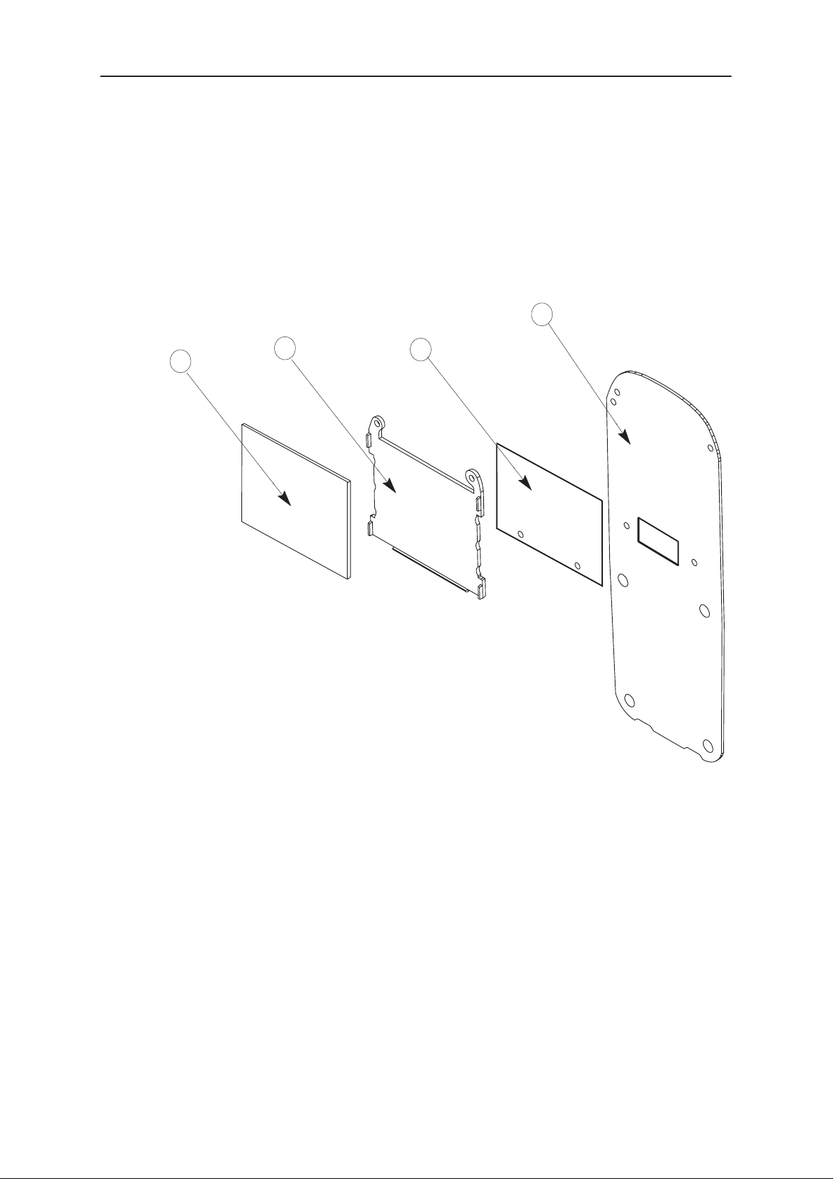
Design
1
4
3
2
1 PCB
2 Reflector tape
3 Lightguide
4 LCD, drawn without TAB
The LCD module CD20 is sub–assembly from LCD manufacturer. It includes the LCD cell and mechanical parts of the module.
Electronics
The following sections of circuitry are included on the UI–PCB.
– Speaker circuit
– Buzzer circuit
– LCD module
– Keyboard and display backlighting circuits
– EMI & ESD circuits for LCD and speaker
Maximum Ratings
Operating temperature range –10... +55 oC
Storage temperature range –40... +85
o
C
Page 3 – 4
Original 10/98
Page 5
PAMS
NHX-7
Technical Documentation
UIF MODULE JE3
DC Characteristics
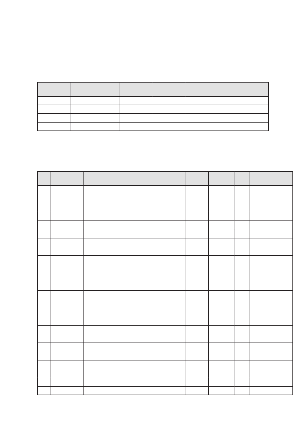
Table 1. Supply Voltages and Power Consumption
Pin / Conn. Line Symbol Minimum Typical /
Nominal
21 VL 2.7 2.85 V
13,14 VBAT 3.0 5.3 V
23, 24 GND 0 V
25, 26 DGND 0 V
Maximum Unit / Notes
The Engine Interface
Table 2. Engine interface, 28–way
Pin Line Sym-
bol
1 ROW0 Keyboard matrix row 0 0 0.2xVL V Low
Parameter Min Typ Max Unit Notes
0.7xVL VL High
2 ROW1 Keyboard matrix row 1 0 0.2xVL V Low
0.7xVL VL High
3 ROW2 Keyboard matrix row 2 0 0.2xVL V Low
0.7xVL VL High
4 ROW3 Keyboard matrix row 3 0 0.2xVL V Low
0.7xVL VL V High
5 COL0 Keyboard matrix column 0 0 0.4 V Low
VL–0.5 VL V High
6 COL1 Keyboard matrix column 1 0 0.4 V Low
VL–0.5 VL V High
7 COL2 Keyboard matrix column 2 0 0.4 V Low
VL–0.5 VL High
8 COL3 Keyboard matrix column 3 0 0.4 V Low
VL–0.5 VL High
9 XPWRON Power on/off detection line
10 GND Analog ground 0 V
11 KEYBLIGHT Illumination control VL–0.5 VL V High / Active
0 0.4 Low
12 LCDBLIGHT Illumination control VL–0.5 VL V High / Active
0 0.4 Low
13 VBATT Battery voltage 3.0 5.3 V
14 VBATT Battery voltage 3.0 5.3 V
Original 10/98
Page 3 – 5
Page 6

NHX-7
PAMS
UIF MODULE JE3
Table 2. Engine interface, 28–way
Pin
bol
15 LCDCLK Display driver clock (external) 80 kHz
VL–0.5 VL V High
0 0.4 V Low
16 SCLK Mux’d LCD serial dataclock Hz
VL–0.5 VL V High
0 0.4 V Low
17 LCDENX Display driver enable 0 0.4 V Low
VL–0.5 VL V High
18 LCDDC Mux’d LCD data or command VL–0.5 VL V High
0 0.4 V Low
19 LCDSDA Mux’d LCD driver serial data 0 0.4 V Low
VL–0.5 VL V High
Technical Documentation
NotesUnitMaxTypMinParameterLine Sym-
20 LCDRES Reset for display driver 0 0.4 V Low
VL–0.5 VL V High
21 VL LCD voltage 2.7 2.85 V
LCD current 5 mA
22 BUZZER Buzzer PWM control 0 2.85 V
23 GND Analog ground 0 V
24 GND Analog ground 0 V
25 DGND Digital ground 0 V
26 DGND Digital ground 0 V
27 EARN Speaker negative 0 1.78 Vpp
28 EARP Speaker positive 0 1.78 Vpp
UIM Connector pads seen from the rear (2/2)
LCD
Page 3 – 6
2815
114
Original 10/98
Page 7
PAMS
NHX-7
Technical Documentation
Functional Description
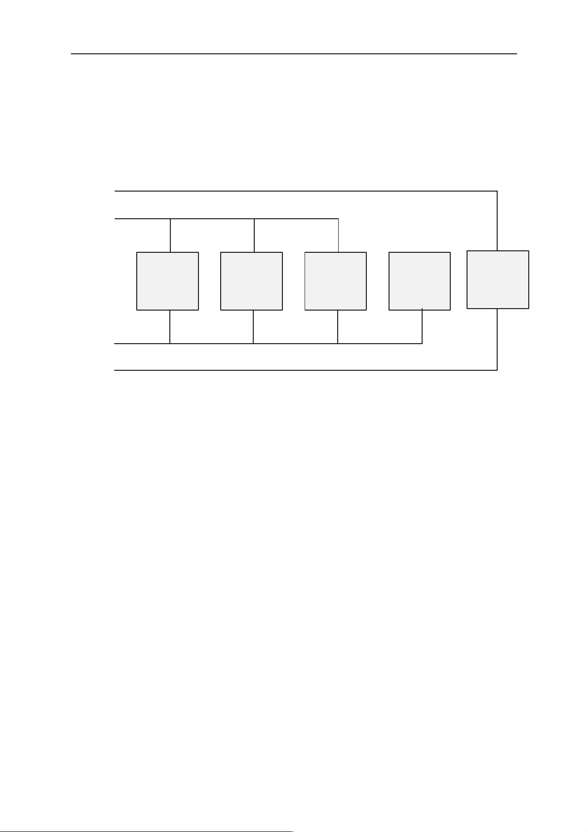
Power Distribution Diagrams
VL
VBATT
Buzzer
GND
LEDs of
Display
LEDs of
Keybord
UIF MODULE JE3
PWR
Display
DGND
Keyboard
Backlight
Figure 1. Power distribution diagram
The keyboard is typed as a matrix pattern. The size of the matrix is 4
rows and 4 columns. The powerkey is separated from matrix. Rows are
connected with pull–up resistors at the MCU.
Switching circuits for backlighting are located on UI board. Display and
keyboard light controls are separated. On system board there is a possibility to control keyboard backlight illumination by i/o line state. Basically
when both lines are in HIGH–state output and lights are bright, black keymat is used. Keyboard control I/O line can be set to INPUT–state to dim
keyboard backlight for white keymat. Dimming scale is controlled at the
system board by resistors.
The leds used for display backlights (6 pc) are side illuminating and are
compatible with CL270–YG. Color of LEDs is yellow–green ( λ 570
nm).
The leds used for keyboard backlights (6 pc) are top illuminating and are
compatible with CL190–YG. Color of LEDs is yellow–green ( λ 570
nm).
Buzzer
The buzzer used is SMD type and controlled by PWM signal, produced by
MCU. Same buzzer is used in DCT3 generation phones.
Original 10/98
Page 3 – 7
Page 8

NHX-7
PAMS
UIF MODULE JE3
Speaker
The speaker circuit includes pads for speaker and a few resistors and
spark caps for EMC circuits. The speaker used is partly open air model
speaker. The most part of the leak holes behind the capsule are closed by
support ring designed. The speaker with the support ring shall be assembled to A–covers specified well. The front resonance well with the
hole of 1.2 mm and partly leaking back cavitation the frequency response
is more constant. Tight contact with the UI–board is needed to ensure
stabile back leak tolerant. Outer ring leak holes are not needed.
LCD
Technical Documentation
Page 3 – 8
Viewing area: ca. 35x24mm
Original 10/98
Page 9

PAMS
NHX-7
Technical Documentation
UIF MODULE JE3
Parts list of JE3 (EDMS Issue 2.4) Code: 0201213
ITEM CODE DESCRIPTION VALUE TYPE
R901 1430035 Chip resistor 1.0 k 5 % 0.063 W 0603
R902 1430087 Chip resistor 100 k 5 % 0.063 W 0603
R903 1430087 Chip resistor 100 k 5 % 0.063 W 0603
R904 1430167 Chip resistor 47 5 % 0.063 W 0603
R911 1430033 Chip resistor 150 k 1 % 0.063 W 0603
R912 1430033 Chip resistor 150 k 1 % 0.063 W 0603
R920 1430043 Chip resistor 2.2 k 5 % 0.063 W 0603
R921 1430053 Chip resistor 5.6 k 5 % 0.063 W 0603
R922 1430155 Chip resistor 15 5 % 0.063 W 0603
R930 1430155 Chip resistor 15 5 % 0.063 W 0603
R931 1430047 Chip resistor 3.3 k 5 % 0.063 W 0603
R932 1430043 Chip resistor 2.2 k 5 % 0.063 W 0603
R950 1430159 Chip resistor 22 5 % 0.063 W 0603
R951 1430144 Chip jumper 0603
R952 1430159 Chip resistor 22 5 % 0.063 W 0603
C904 2320045 Ceramic cap. 27 p 5 % 50 V 0603
C910 2312401 Ceramic cap. 1.0 u 10 % 10 V 0805
C911 2320779 Ceramic cap. 100 n 10 % 16 V 0603
C912 2320779 Ceramic cap. 100 n 10 % 16 V 0603
C913 2320779 Ceramic cap. 100 n 10 % 16 V 0603
C914 2320779 Ceramic cap. 100 n 10 % 16 V 0603
C915 2320779 Ceramic cap. 100 n 10 % 16 V 0603
C916 2312401 Ceramic cap. 1.0 u 10 % 10 V 0805
C917 2312401 Ceramic cap. 1.0 u 10 % 10 V 0805
C918 2320107 Ceramic cap. 10 n 5 % 50 V 0603
B904 5140087 Buzzer 85db 2600hz 3.6v 10x10x3.5
Z001 3640035 Filt z>450r/100m 0r7max 0.2a 0603
Z002 3640035 Filt z>450r/100m 0r7max 0.2a 0603
H910 4850061 LCD display module 5x7dotmx30+cui+driver
V001 4864388 Led Green 0603
V002 4864388 Led Green 0603
V003 4864388 Led Green 0603
V004 4860005 Led Green 0603
V005 4860005 Led Green 0603
V009 4864388 Led Green 0603
V010 4864388 Led Green 0603
V012 4864388 Led Green 0603
V017 4860005 Led Green 0603
V020 4860005 Led Green 0603
V021 4860005 Led Green 0603
V022 4860005 Led Green 0603
V901 4210100 Transistor BC848W npn 30 V SOT323
V902 4200875 Transistor BCX54–16 npn 45 V 1.5 A SOT89
Original 10/98
Page 3 – 9
Page 10

NHX-7
PAMS
UIF MODULE JE3
V904 4100278 Diode x 2 BAV7070 V 200 mA COMCAT .SOT23
V920 4200836 Transistor BCX19 npn 50 V 0.5 A SOT23
V930 4200836 Transistor BCX19 npn 50 V 0.5 A SOT23
9854321 PCB JE3 41.0X113.1X0.8 D 4/PA
Technical Documentation
Page 3 – 10
Original 10/98
Page 11

PAMS
NHX-7
Technical Documentation
UIF MODULE JE3
This page intentionally left blank.
Original 10/98
Page 3 – 11
Page 12

NHX-7
PAMS
UIF MODULE JE3
Technical Documentation
This page intentionally left blank.
Page 3 – 12
Original 10/98
 Loading...