

Page 1

After Sales Technical Documentation
NHN–3N Series Transceivers
Chapter 1
RF Block
Original 43/96
Page 2

NHN–3N
After Sales
RF Block
Technical Documentation
CONTENTS
Introduction 4 – 3. . . . . . . . . . . . . . . . . . . . . . . . . . . . . . . . . . . . . . . . . . . . . . . . . . . . . .
Technical Summary 4 – 3. . . . . . . . . . . . . . . . . . . . . . . . . . . . . . . . . . . . . . . . . . . .
Functional Description 4 – 3. . . . . . . . . . . . . . . . . . . . . . . . . . . . . . . . . . . . . . . . .
Basic Specifications 4 – 3. . . . . . . . . . . . . . . . . . . . . . . . . . . . . . . . . . . . . . . .
Module Characteristics 4 – 4. . . . . . . . . . . . . . . . . . . . . . . . . . . . . . . . . . . . . . . . .
Maximum ratings 4 – 4. . . . . . . . . . . . . . . . . . . . . . . . . . . . . . . . . . . . . . . . . . .
DC Characteristics 4 – 4. . . . . . . . . . . . . . . . . . . . . . . . . . . . . . . . . . . . . . . . .
Connections 4 – 4. . . . . . . . . . . . . . . . . . . . . . . . . . . . . . . . . . . . . . . . . . . . . . . . . .
Connections to Baseband module 4 – 4. . . . . . . . . . . . . . . . . . . . . . . . . . . .
Digital control signal values 4 – 5. . . . . . . . . . . . . . . . . . . . . . . . . . . . . . . . . .
Block diagram 4 – 9. . . . . . . . . . . . . . . . . . . . . . . . . . . . . . . . . . . . . . . . . . . . .
RF components 4 – 10. . . . . . . . . . . . . . . . . . . . . . . . . . . . . . . . . . . . . . . . . . . .
Receiver 4 – 10. . . . . . . . . . . . . . . . . . . . . . . . . . . . . . . . . . . . . . . . . . . . . . . . . .
RX Synthesizer 4 – 10. . . . . . . . . . . . . . . . . . . . . . . . . . . . . . . . . . . . . . . . . . . .
RX loop filter 4 – 11. . . . . . . . . . . . . . . . . . . . . . . . . . . . . . . . . . . . . . . . . . . . . . .
TX Synthesizer 4 – 11. . . . . . . . . . . . . . . . . . . . . . . . . . . . . . . . . . . . . . . . . . . .
TX Loop Filter 4 – 11. . . . . . . . . . . . . . . . . . . . . . . . . . . . . . . . . . . . . . . . . . . . .
Transmitter 4 – 11. . . . . . . . . . . . . . . . . . . . . . . . . . . . . . . . . . . . . . . . . . . . . . . .
Regulators 4 – 12. . . . . . . . . . . . . . . . . . . . . . . . . . . . . . . . . . . . . . . . . . . . . . . .
AFC function 4 – 12. . . . . . . . . . . . . . . . . . . . . . . . . . . . . . . . . . . . . . . . . . . . . .
Parts List of JR8 EDMS Issue 3.2 4 – 13. . . . . . . . . . . . . . . . . . . . . . . . . . . . . . .
Page 1 – 2
Original 43/96
Page 3
After Sales
NHN–3N
Technical Documentation
Introduction
Technical Summary
Functional Description
The RF module is designed for handportable cellular phone which operates in the NMT900 system. The purpose of the module is to receive and
demodulate the radio frequency signal from base station and transmit
modulated RF signal to base station.
RF module is constructed on a 1.0 mm thick FR4 four–layer Printed Wire
Board. Dimensions of the PWB are 142 mm x 48 mm.
EMC leakage is prevented with magnesium shield on component side.
RF Block
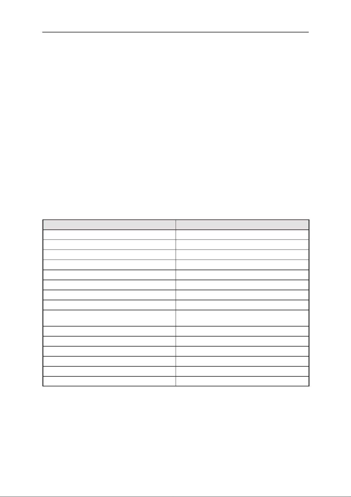
Basic Specifications
Parameter Value
RX frequency band 935.0125 – 959.9875 MHz
TX frequency band 890.0125 – 914.9875 MHz
RX LO frequency band 980.0125 – 1004.9875 MHz
Duplex spacing 45 MHz
Channel numbers 1 – 1000, 1025 – 2023
Number of channels 1999
Channel spacing 12.5/25 kHz
TX output power 0.1 W low power, 0.55 W high power
Method of frequency synthesis Dual PLL with two UHF signals for RX LO and
TX
Frequency control AFC with +/– 2.5 kHz limits
Receiver type Superheterodyne with double IF
Modulator type FM–modulator
Current consumption, reception 63 mA
Current consumption, standby
Current consumption, transmission 570 mA
Original 43/96
Page 1 – 3
Page 4
NHN–3N
After Sales
RF Block
Technical Documentation
Module Characteristics
Maximum ratings
The maximum battery voltage during transmission should not exceed 6.0
V. Higher battery voltages may destroy the power amplifier module.
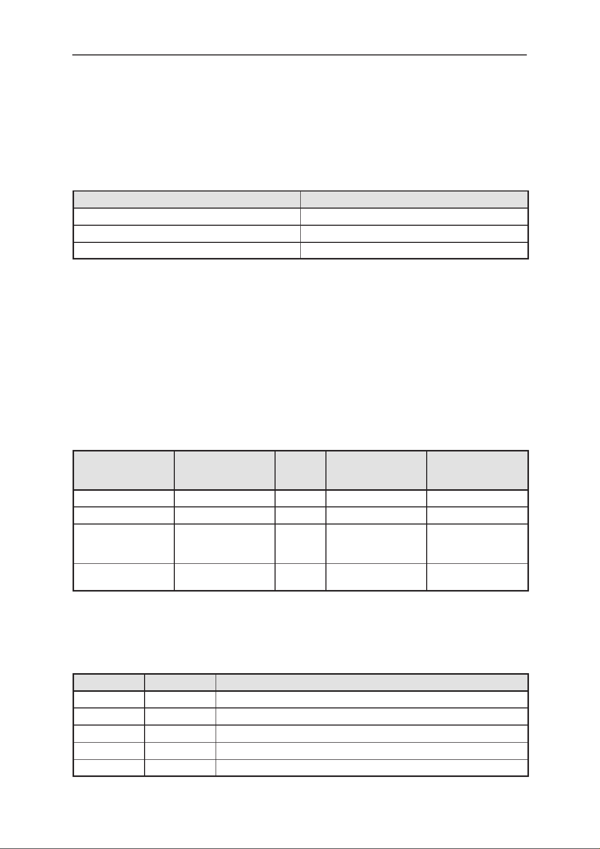
Parameter Value
Battery voltage nom. 4.8 V, min. 4.5 V, max. 6.0 V,
Regulated supply voltage 3.6 V +/– 5 %
Operating temperature range –25 ... +55 deg.C
DC Characteristics
Regulators
There are two regulators in the RF unit. Regulators get their reference
voltages 3.3 V (Vref) from BB unit. Regulators regulate the battery voltage
to the fixed 3.6 V level.
Control Signals
In the following table the RF current consumption can be seen with different status of the control signals. RX and TX synthesizer phase locked
loops are switched on/off by a control byte of PLL circuit.
RXE + SW powerup for RX synthe-
sizer
H H H 550 mA Power Level 2
H H L 84 mA
H L L 47 mA Synthesizer TX part
L L L 1 mA All RF parts have
TXS + SW powerup for TX synthe-
sizer
TXE Typical Current
Consumption /mA
has been powered
off
been powered off
Connections
Connections to Baseband module
Signal Name Type Function
Note
AFC Analog out The reference oscillator frequency adjust.
AGC Digital out Receiver gain control. Active state: High
DAF Analog in Demodulated received signal (audio + fii+ data)
GND Power Common ground
IF Analog out 2nd IF signal (450 kHz)
Page 1 – 4
Original 43/96
Page 5
After Sales
NHN–3N
Technical Documentation
FunctionTypeSignal Name
MOD Analog out Modulation signal for transmitter (audio + fii + data)
RFTEMP Analog in Main crystal temperature.
RSSI Analog in Received signal strength indicator. Voltage measurement.
RXE Digital out Receiver enable, Active state: High
SCLK Digital out Serial clock for synthesizer. Active state: Rising edge
SDAT Digital out Serial data for synthesizer. Active state: High
SLE Digital out Synthesizer latch enable
TXC PWM out Transmitter power control
TXE Digital out Transmitter enable. Active state: High
TXI Analog in ”TX power on” –indicator
TXS Digital out TX synthesizer enable. Active state: High
VBAT Power Battery voltage to transmitter
VRF Power Battery voltage to regulator
RF Block
VREF Power Reference voltage
Digital control signal values
Supply voltage VDD 3.3 V
Logical 1 VOH >VDD*0,7
Logical 0 VOL <VDD*0,3
Logical 1 IOH <1mA , 1A (typical)
Logical 0 IOL <1mA , 1A (typical)
AFC VCTCXO control voltage
Type analog signal (DC–level)
Level 0.3...3,0 V DC
Source impedance Zs < 1.5 kohm
Load impedance ZL > 10 kohm
Control step size for TX freq. 100 Hz (typical)
AGC Receiver gain control
Type Digital signal
Function 0 = AGC off
1 = AGC on
Original 43/96
Page 1 – 5
Page 6
NHN–3N
After Sales
RF Block
DAF Demodulated audio and data
signal
Type analog signal
Nominal level 50 mVrms @3,0 kHz deviation
Unit to unit variation 35 mV...65 mV
Source impedance ZS < 5 kohm
Load impedance ZL > 50 kohm
IF 450 kHz 2nd IF signal
Level 250 mVpp (typical) not speci-
Source impedance < 10 k W
Load impedance > 50 k W
Technical Documentation
fied by manufacturer
MOD Modulation signal for trans-
mitter (Audio + data)
Type Analog signal
Nominal level 300 mVpp @3,0 kHz deviation
Load impedance ZL > 10 kW
Source impedance Zs < 5 kW
RFTEMP VCTCXO temperature
Type analog signal
Level 0...3,3 V DC
Temp. range –25...+55 degrees centigrade
RSSI Received signal strength in-
dicator
DC–level 0.2...3.0 V
Source impedance 56 kW (typical)
RXE Receiver enable
Type Digital signal
Function 0 = RX off
1 = RX on
On–state current 150 mA (typical) (300 mA max.)
Page 1 – 6
Original 43/96
Page 7
After Sales
NHN–3N
Technical Documentation
SCLK Serial clock for synthesizer
Type digital signal
Pulse width > 1 us
SLE Synthesizer enable
Type Digital signal
TXC Transmitter power control
Type PWM signal
Function Duty cycle of the TXC signal
defines the TX power level
PWM frequency 5 kHz
RF Block
Level 0...3.3 V DC
Number of duty cycle steps 256
Load impedance > 100 kohm
TXE Transmitter on/off control
Type Digital signal
Function 0 = TX off
1 = TX on
TXI ”TX power on” –indicator
Type Analog signal
Source impedance > 47 kW
Level < 1 V = TX off
> 1 V = TX on
TXS TX synthesizer on/off
Type Digital signal
Function 0 = Supply off
1 = Supply on
Original 43/96
Page 1 – 7
Page 8

NHN–3N
After Sales
RF Block
VBAT Battery voltage
Nominal value 4.8 V
Minimum value 4.5 V
Absolute maximum 6.9 V
Max. current 700 mA
VRF Battery voltage for RX regula-
tor
Nominal value 4.8 V
Minimum value 4.5 V
Absolute maximum 6.9 V
Max. current 100 mA
Technical Documentation
VREF Reference voltage
Level 3.3 V 4%
Page 1 – 8
Original 43/96
Page 9

After Sales
NHN–3N
Technical Documentation
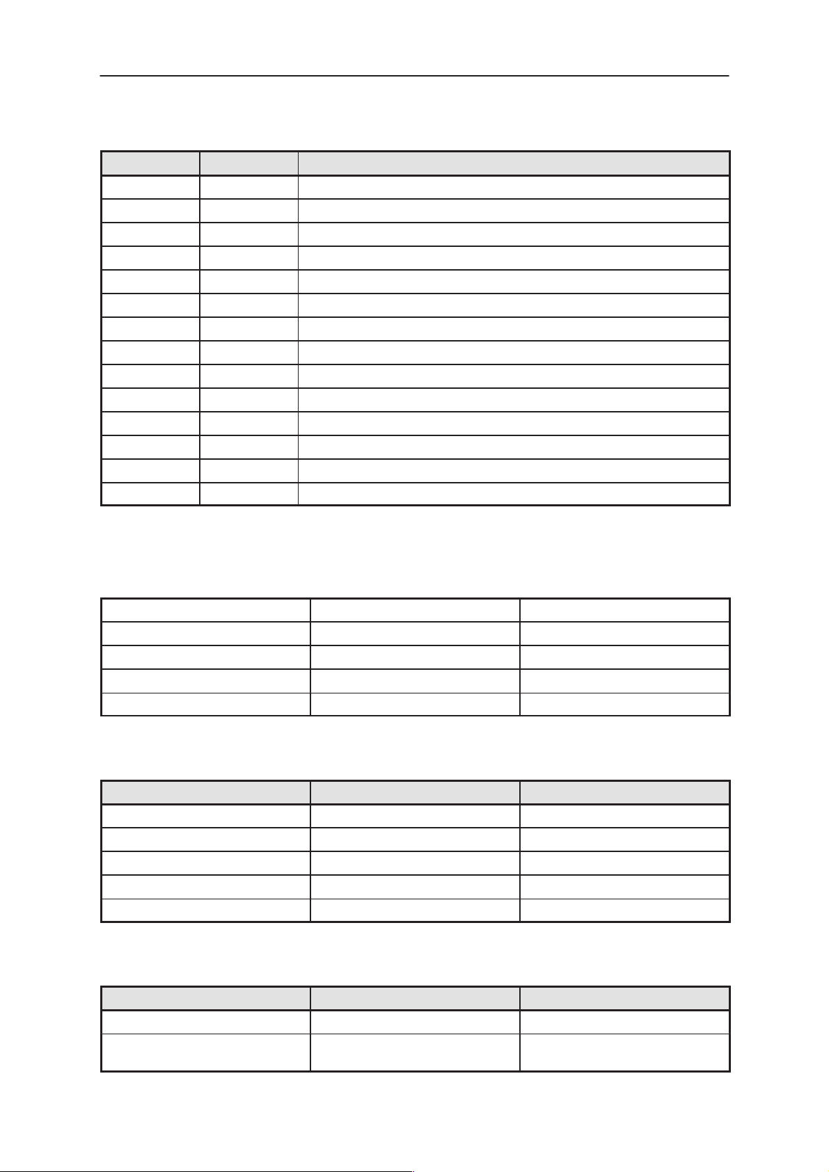
Block diagram
DAF
IF
RSSI
450 kHz FILTER
IF CIRCUIT
TX LO BUFFER
PHASE SHIFTER
TX VCO
LOOP FILTER
MOD
SLE
SCLK
AGC
SDATA
RF TEMP
AFC
TXC
VCTCXO 14.85 MHz
TXE
TXI
VBAT
REGULATOR
3.6 V
VCCR
VTSYN TSYN SWITCH
RF Block
VREF
REGULATOR
3.6 V
VSYN
TXS
IF AMPLIFIER
45 MHz
CRYSTAL FILTER
DIODE MIXER
RX–FILTER
LNA
UMA 1015
SYNTHESIZER IC
TANK CIRCUIT FOR 2.ND LO
PLL
PLL
LOOP FILTER
RX LO BUFFER
RX VCO
RF2131
AMPLIFIER MODULE
TX POWER CONTROL
POWER DETECTOR
Original 43/96
ANTENNA
DUPLEX–FILTER
DIR_COUPLER
Page 1 – 9
Page 10

NHN–3N
After Sales
RF Block
Receiver
Technical Documentation
The receiver is a dual–conversion superheterodyne using two intermediate
frequencies, 45 MHz and 450 kHz.
The RF signal from the duplexer RX port is applied to the RF amplifier. The
amplifier has 18 dB gain and 1,5 dB noise figure.
Next the signal is filtered with Z321. The filter is followed by a single balanced
diode mixer, which has 6 dB conversion loss.
After the mixer signal is filtered with the crystal filter Z350, which has 7,5 kHz
bandwidth. Next the IF signal is amplified by V380. From the amplifier the
IF–signal is applied to the second mixer.
The second mixer, the LO buffer transistor, IF amplifier and quadrature
detector are all integrated in the circuit N370. The second LO frequency,
44.55 MHz, is third harmonic of the VCTCXO frequency . LO signal is realized
with tank circuit C372 and L371. After the mixer the 450kHz IF signal is
filtered with ceramic filter Z370. The IF amplifier output signal is phase
shifted by resonance circuit. After this the signal is fed to a quadrature
detector.
Signal DAF is low pass filtered by R372 and C379. The DAF, RSSI and 2nd
IF signal (450 kHz) are fed to the audio/logic unit.
RX Synthesizer
The first injection frequency for receiver is generated by a digital phase
locked loop (PLL). The output frequency of the loop (LO) is obtained from
a voltage–controlled oscillator (VCO) G530. The VCO output signal is
amplified by RX–LO–buffer and fed to the receiver mixer . The injection level
required by the receiver mixer is about +3 dBm. In addition, the signal is
feeded back to the dualsynthesizer circuit N820.
The overall divisor of the chain is selected according to the desired channel.
The internal dividers of N820 are programmed with 17 bits, which are
transferred serially on the SDAT (synthesizer data) line from the processor
into an internal shift register also located in N820. Data transfer is timed with
SCLK clock pulses.
The divided frequency is compared with a highly stable reference frequency
by a phase comparator in the PLL circuit. The phase comparator controls the
VCO frequency by means of a DC voltage through the loop filter so as to keep
the divided frequency applied to the phase comparator equal to the fixed
reference frequency.
The reference frequency is 12,5 kHz. This reference frequency is obtained
from voltage controlled crystal oscillator (VCXO or VCTCXO). Oscillator
frequency is 14.85 MHz. The VCXO frequency is divided by 1188.
RX loop filter
Phase comparator output is pin 3. If the VCO frequency is too high, the
output goes low and discharge integrator capacitor C521. After this, the DC
control voltage and the VCO frequency will decrease.
Page 1 – 10
Original 43/96
Page 11

After Sales
NHN–3N
Technical Documentation
If the VCO frequency is too low, the output goes high and charge the
integrator capacitor C521. Thereafter the DC control voltage and the VCO
frequency will go up.
Output pulses from the phase detector have to be supplied to the loop filter.
The function of the integrator is to convert positive and negative pulses to DC
voltage. The remaining ripple and AC components are filtered in the lowpass
filter.
TX Synthesizer
The transmitter synthesizer generates a frequency modulated transmitter
signal for the transmitter section. The modulated TX injection frequency is
generated in TX–VCO (G430). The TX modulated TX signal is amplified in
TX–buffer before the transmitter.
TX Loop Filter
Output pulses from the phase detector N820 pin 17 have to be supplied to
the loop filter. The integrator, which is constituted of R420 and C421,
converts positive and negative pulses to DC voltage. The remaining ripple
is filtered in the low–pass filter.
RF Block
Transmitter
The transmitter is realized with a power amplifier module. The modulated RF
signal from the TX synthesizer is applied to the 50 ohm input of the module.
The power level is controlled by the voltage supplied to the pin 1. Zener diode
V642 protects the module against too high control voltages (>4.5 V).
Amplifier module has two pairs of output pins ( pins 10, 11 and 14,15 ).
Amplified RF signals are compined symmetrically and fed through a
low–pass filter to the duplex filter. The harmonics of the transmitter are
reduced by the duplex filter. A voltage proportional to the output power is
rectified from a directional coupler by DC–biased Schottky diode V640. This
rectified voltage is fed to a differential amplifier which consists of transistor
V650. The reference voltage is filtered from the PWM signal by TXC line. The
differential amplifier adjusts the control voltage so that the reference voltage
and the voltage proportional to the output power are equal. The transmitter
is switched on when TXE goes high (logic 1), which enables the transmitter
power control circuit by transistor V653. When the transmitter is inactive
(TXE low) the RF level from the transmitter is reduced below –57 dBm.
Regulators
The voltage regulators for RF parts consist of the transistors V310, 31 1, 313
and 314. The first regulator (V310, 311) provides the operating voltage for
the receiver, PLL circuit and RX–VCO buffer. The other one is used to
regulate the operating voltage of the RX–VCO. These regulators are
realized using discrete transistors because the output noise has to be very
low. The 3.3 V reference voltage (VREF) is fed from the logic module. TX
synthesizer gets the supply voltage via a switch which is realized using
transistors V411 and V410. The switch is controlled by the digital TXS–line
from the logic module.
Original 43/96
Page 1 – 11
Page 12

NHN–3N
After Sales
RF Block
AFC function
The transceiver unit is equipped with AFC function, i.e. it uses the incoming
receive signal from base station as a frequency reference. The control loop
consists of the receiver, the IF counter in the NIPA, CPU, an 8–bit D/A
converter in the NIPA and the VCTCXO, which is used as a reference
oscillator for the synthesizer.
The 2nd IF signal (450 kHz) from receiver is fed to the NIP A. The IF counter
counts the received frequency. If the frequency differs from programmed
value, CPU adjusts the frequency of the VCXO by changing output voltage
of the D/A converter. This adjustment continues until the desired receive
frequency is achieved. AFC is not active during a channel scan and below
–90 dBm RX signal level.
Technical Documentation
Page 1 – 12
Original 43/96
Page 13

After Sales
NHN–3N
Technical Documentation
RF Block
Parts List of JR8 EDMS Issue 3.5 (for layout version 06) Code: 0200863
ITEM CODE DESCRIPTION VALUE TYPE
R111 1430804 Chip resistor 100 k 5 % 0.063 W 0402
R112 1430786 Chip resistor 18 k 5 % 0.063 W 0402
R113 1430796 Chip resistor 47 k 5 % 0.063 W 0402
R114 1430754 Chip resistor 1.0 k 5 % 0.063 W 0402
R115 1430738 Chip resistor 270 5 % 0.063 W 0402
R116 1430804 Chip resistor 100 k 5 % 0.063 W 0402
R117 1430788 Chip resistor 22 k 5 % 0.063 W 0402
R118 1430770 Chip resistor 4.7 k 5 % 0.063 W 0402
R119 1430730 Chip resistor 150 5 % 0.063 W 0402
R120 1430764 Chip resistor 3.3 k 5 % 0.063 W 0402
R121 1430778 Chip resistor 10 k 5 % 0.063 W 0402
R122 1430780 Chip resistor 12 k 5 % 0.063 W 0402
R123 1430780 Chip resistor 12 k 5 % 0.063 W 0402
R124 1430778 Chip resistor 10 k 5 % 0.063 W 0402
R151 1430754 Chip resistor 1.0 k 5 % 0.063 W 0402
R155 1430754 Chip resistor 1.0 k 5 % 0.063 W 0402
R161 1430770 Chip resistor 4.7 k 5 % 0.063 W 0402
R162 1430770 Chip resistor 4.7 k 5 % 0.063 W 0402
R163 1430740 Chip resistor 330 5 % 0.063 W 0402
R171 1430726 Chip resistor 100 5 % 0.063 W 0402
R202 1430796 Chip resistor 47 k 5 % 0.063 W 0402
R203 1430778 Chip resistor 10 k 5 % 0.063 W 0402
R204 1430796 Chip resistor 47 k 5 % 0.063 W 0402
R205 1430778 Chip resistor 10 k 5 % 0.063 W 0402
R208 1430770 Chip resistor 4.7 k 5 % 0.063 W 0402
R242 1430792 Chip resistor 33 k 5 % 0.063 W 0402
R243 1430792 Chip resistor 33 k 5 % 0.063 W 0402
R245 1430770 Chip resistor 4.7 k 5 % 0.063 W 0402
R247 1430804 Chip resistor 100 k 5 % 0.063 W 0402
R251 1430792 Chip resistor 33 k 5 % 0.063 W 0402
R252 1430792 Chip resistor 33 k 5 % 0.063 W 0402
R263 1800673 NTC resistor 15 k 10 % 0.12 W 0805
R310 1430778 Chip resistor 10 k 5 % 0.063 W 0402
R311 1430778 Chip resistor 10 k 5 % 0.063 W 0402
R312 1430778 Chip resistor 10 k 5 % 0.063 W 0402
R313 1430758 Chip resistor 1.5 k 5 % 0.063 W 0402
R314 1430778 Chip resistor 10 k 5 % 0.063 W 0402
R315 1430776 Chip resistor 8.2 k 5 % 0.063 W 0402
R317 1430778 Chip resistor 10 k 5 % 0.063 W 0402
R318 1430786 Chip resistor 18 k 5 % 0.063 W 0402
R320 1430754 Chip resistor 1.0 k 5 % 0.063 W 0402
R321 1430786 Chip resistor 18 k 5 % 0.063 W 0402
R322 1430726 Chip resistor 100 5 % 0.063 W 0402
Original 43/96
Page 1 – 13
Page 14

NHN–3N
After Sales
RF Block
R325 1430778 Chip resistor 10 k 5 % 0.063 W 0402
R326 1430758 Chip resistor 1.5 k 5 % 0.063 W 0402
R327 1430776 Chip resistor 8.2 k 5 % 0.063 W 0402
R328 1430778 Chip resistor 10 k 5 % 0.063 W 0402
R330 1430754 Chip resistor 1.0 k 5 % 0.063 W 0402
R331 1430808 Chip resistor 150 k 5 % 0.063 W 0402
R332 1430734 Chip resistor 220 5 % 0.063 W 0402
R333 1430700 Chip resistor 10 5 % 0.063 W 0402
R334 1430710 Chip resistor 22 5 % 0.063 W 0402
R335 1430764 Chip resistor 3.3 k 5 % 0.063 W 0402
R340 1430780 Chip resistor 12 k 5 % 0.063 W 0402
R341 1430832 Chip resistor 2.7 k 5 % 0.063 W 0402
R342 1430700 Chip resistor 10 5 % 0.063 W 0402
R343 1430734 Chip resistor 220 5 % 0.063 W 0402
R350 1430726 Chip resistor 100 5 % 0.063 W 0402
R360 1430744 Chip resistor 470 5 % 0.063 W 0402
R361 1430778 Chip resistor 10 k 5 % 0.063 W 0402
R362 1430778 Chip resistor 10 k 5 % 0.063 W 0402
R363 1430756 Chip resistor 1.2 k 5 % 0.063 W 0402
R365 1430690 Chip jumper 0402
R366 1430714 Chip resistor 33 5 % 0.063 W 0402
R370 1430758 Chip resistor 1.5 k 5 % 0.063 W 0402
R371 1430770 Chip resistor 4.7 k 5 % 0.063 W 0402
R372 1430754 Chip resistor 1.0 k 5 % 0.063 W 0402
R373 1430714 Chip resistor 33 5 % 0.063 W 0402
R374 1430804 Chip resistor 100 k 5 % 0.063 W 0402
R381 1430770 Chip resistor 4.7 k 5 % 0.063 W 0402
R411 1430778 Chip resistor 10 k 5 % 0.063 W 0402
R412 1430786 Chip resistor 18 k 5 % 0.063 W 0402
R413 1430778 Chip resistor 10 k 5 % 0.063 W 0402
R414 1430778 Chip resistor 10 k 5 % 0.063 W 0402
R420 1430766 Chip resistor 3.9 k 5 % 0.063 W 0402
R421 1430754 Chip resistor 1.0 k 5 % 0.063 W 0402
R422 1430770 Chip resistor 4.7 k 5 % 0.063 W 0402
R423 1430778 Chip resistor 10 k 5 % 0.063 W 0402
R430 1430718 Chip resistor 47 5 % 0.063 W 0402
R431 1430734 Chip resistor 220 5 % 0.063 W 0402
R432 1430788 Chip resistor 22 k 5 % 0.063 W 0402
R433 1430786 Chip resistor 18 k 5 % 0.063 W 0402
R434 1430700 Chip resistor 10 5 % 0.063 W 0402
R440 1430762 Chip resistor 2.2 k 5 % 0.063 W 0402
R441 1430772 Chip resistor 5.6 k 5 % 0.063 W 0402
R442 1430734 Chip resistor 220 5 % 0.063 W 0402
R443 1430700 Chip resistor 10 5 % 0.063 W 0402
R520 1430764 Chip resistor 3.3 k 5 % 0.063 W 0402
R521 1430754 Chip resistor 1.0 k 5 % 0.063 W 0402
R522 1430770 Chip resistor 4.7 k 5 % 0.063 W 0402
Technical Documentation
Page 1 – 14
Original 43/96
Page 15

After Sales
NHN–3N
Technical Documentation
R523 1430778 Chip resistor 10 k 5 % 0.063 W 0402
R530 1430724 Chip resistor 82 5 % 0.063 W 0402
R531 1430734 Chip resistor 220 5 % 0.063 W 0402
R532 1430700 Chip resistor 10 5 % 0.063 W 0402
R601 1430700 Chip resistor 10 5 % 0.063 W 0402
R632 1430700 Chip resistor 10 5 % 0.063 W 0402
R641 1430726 Chip resistor 100 5 % 0.063 W 0402
R642 1430796 Chip resistor 47 k 5 % 0.063 W 0402
R643 1430786 Chip resistor 18 k 5 % 0.063 W 0402
R644 1430754 Chip resistor 1.0 k 5 % 0.063 W 0402
R646 1430776 Chip resistor 8.2 k 5 % 0.063 W 0402
R647 1430744 Chip resistor 470 5 % 0.063 W 0402
R649 1430806 Chip resistor 120 k 5 % 0.063 W 0402
R651 1430796 Chip resistor 47 k 5 % 0.063 W 0402
R652 1430786 Chip resistor 18 k 5 % 0.063 W 0402
R653 1430754 Chip resistor 1.0 k 5 % 0.063 W 0402
R654 1430778 Chip resistor 10 k 5 % 0.063 W 0402
R656 1430796 Chip resistor 47 k 5 % 0.063 W 0402
R657 1430796 Chip resistor 47 k 5 % 0.063 W 0402
R659 1430778 Chip resistor 10 k 5 % 0.063 W 0402
R660 1430690 Chip jumper 0402
R721 1430754 Chip resistor 1.0 k 5 % 0.063 W 0402
R722 1430776 Chip resistor 8.2 k 5 % 0.063 W 0402
R731 1430762 Chip resistor 2.2 k 5 % 0.063 W 0402
R741 1430770 Chip resistor 4.7 k 5 % 0.063 W 0402
R742 1430796 Chip resistor 47 k 5 % 0.063 W 0402
R743 1430796 Chip resistor 47 k 5 % 0.063 W 0402
R767 1430778 Chip resistor 10 k 5 % 0.063 W 0402
R768 1430786 Chip resistor 18 k 5 % 0.063 W 0402
R771 1430762 Chip resistor 2.2 k 5 % 0.063 W 0402
R772 1430151 Chip resistor 10 5 % 0.063 W 0603
R773 1430151 Chip resistor 10 5 % 0.063 W 0603
R800 1800673 NTC resistor 15 k 10 % 0.12 W 0805
R811 1430778 Chip resistor 10 k 5 % 0.063 W 0402
R812 1430754 Chip resistor 1.0 k 5 % 0.063 W 0402
R816 1430700 Chip resistor 10 5 % 0.063 W 0402
R820 1430786 Chip resistor 18 k 5 % 0.063 W 0402
R821 1430714 Chip resistor 33 5 % 0.063 W 0402
R822 1430714 Chip resistor 33 5 % 0.063 W 0402
R826 1430786 Chip resistor 18 k 5 % 0.063 W 0402
R829 1430778 Chip resistor 10 k 5 % 0.063 W 0402
R830 1430778 Chip resistor 10 k 5 % 0.063 W 0402
R831 1430778 Chip resistor 10 k 5 % 0.063 W 0402
R840 1430714 Chip resistor 33 5 % 0.063 W 0402
R900 1430087 Chip resistor 100 k 5 % 0.063 W 0603
R901 1430077 Chip resistor 39 k 5 % 0.063 W 0603
R902 1430087 Chip resistor 100 k 5 % 0.063 W 0603
RF Block
Original 43/96
Page 1 – 15
Page 16

NHN–3N
After Sales
RF Block
R903 1800673 NTC resistor 15 k 10 % 0.12 W 0805
R904 1430051 Chip resistor 4.7 k 5 % 0.063 W 0603
R909 1430151 Chip resistor 10 5 % 0.063 W 0603
R920 1430762 Chip resistor 2.2 k 5 % 0.063 W 0402
R921 1430762 Chip resistor 2.2 k 5 % 0.063 W 0402
R922 1430718 Chip resistor 47 5 % 0.063 W 0402
R923 1430710 Chip resistor 22 5 % 0.063 W 0402
R924 1430710 Chip resistor 22 5 % 0.063 W 0402
R930 1430804 Chip resistor 100 k 5 % 0.063 W 0402
C101 2611668 Tantalum cap. 4.7 u 20 % 10 V 3.2x1.6x1.6
C102 2320620 Ceramic cap. 10 n 5 % 16 V 0402
C103 2310791 Ceramic cap. 33 n 20 % 50 V 0805
C104 2320620 Ceramic cap. 10 n 5 % 16 V 0402
C105 2604199 Tantalum cap. 2.2 u 20 % 3.2x1.6x1.6
C106 2604199 Tantalum cap. 2.2 u 20 % 3.2x1.6x1.6
C107 2604199 Tantalum cap. 2.2 u 20 % 3.2x1.6x1.6
C108 2320620 Ceramic cap. 10 n 5 % 16 V 0402
C109 2320620 Ceramic cap. 10 n 5 % 16 V 0402
C111 2320620 Ceramic cap. 10 n 5 % 16 V 0402
C112 2604209 Tantalum cap. 1.0 u 20 % 16 V 3.2x1.6x1.6
C113 2320620 Ceramic cap. 10 n 5 % 16 V 0402
C120 2320546 Ceramic cap. 27 p 5 % 50 V 0402
C121 2320546 Ceramic cap. 27 p 5 % 50 V 0402
C122 2320546 Ceramic cap. 27 p 5 % 50 V 0402
C123 2320546 Ceramic cap. 27 p 5 % 50 V 0402
C140 2320620 Ceramic cap. 10 n 5 % 16 V 0402
C141 2320584 Ceramic cap. 1.0 n 5 % 50 V 0402
C142 2604209 Tantalum cap. 1.0 u 20 % 16 V 3.2x1.6x1.6
C143 2320546 Ceramic cap. 27 p 5 % 50 V 0402
C161 2320546 Ceramic cap. 27 p 5 % 50 V 0402
C191 2320584 Ceramic cap. 1.0 n 5 % 50 V 0402
C192 2320584 Ceramic cap. 1.0 n 5 % 50 V 0402
C193 2320584 Ceramic cap. 1.0 n 5 % 50 V 0402
C194 2320584 Ceramic cap. 1.0 n 5 % 50 V 0402
C195 2320584 Ceramic cap. 1.0 n 5 % 50 V 0402
C201 2307816 Ceramic cap. 47 n 20 % 25 V 0805
C202 2307816 Ceramic cap. 47 n 20 % 25 V 0805
C203 2307816 Ceramic cap. 47 n 20 % 25 V 0805
C205 2320620 Ceramic cap. 10 n 5 % 16 V 0402
C206 2320620 Ceramic cap. 10 n 5 % 16 V 0402
C228 2320620 Ceramic cap. 10 n 5 % 16 V 0402
C229 2320620 Ceramic cap. 10 n 5 % 16 V 0402
C241 2307816 Ceramic cap. 47 n 20 % 25 V 0805
C242 2307816 Ceramic cap. 47 n 20 % 25 V 0805
C251 2307816 Ceramic cap. 47 n 20 % 25 V 0805
C312 2320598 Ceramic cap. 3.9 n 5 % 50 V 0402
C313 2604209 Tantalum cap. 1.0 u 20 % 16 V 3.2x1.6x1.6
Technical Documentation
Page 1 – 16
Original 43/96
Page 17

After Sales
NHN–3N
Technical Documentation
C314 2611668 Tantalum cap. 4.7 u 20 % 10 V 3.2x1.6x1.6
C315 2611668 Tantalum cap. 4.7 u 20 % 10 V 3.2x1.6x1.6
C320 2320546 Ceramic cap. 27 p 5 % 50 V 0402
C322 2320546 Ceramic cap. 27 p 5 % 50 V 0402
C323 2320518 Ceramic cap. 1.8 p 0.25 % 50 V 0402
C324 2320546 Ceramic cap. 27 p 5 % 50 V 0402
C325 2320534 Ceramic cap. 8.2 p 0.25 % 50 V 0402
C326 2320546 Ceramic cap. 27 p 5 % 50 V 0402
C327 2320526 Ceramic cap. 3.9 p 0.25 % 50 V 0402
C328 2611668 Tantalum cap. 4.7 u 20 % 10 V 3.2x1.6x1.6
C331 2320620 Ceramic cap. 10 n 5 % 16 V 0402
C332 2320584 Ceramic cap. 1.0 n 5 % 50 V 0402
C333 2320584 Ceramic cap. 1.0 n 5 % 50 V 0402
C340 2320520 Ceramic cap. 2.2 p 0.25 % 50 V 0402
C341 2320546 Ceramic cap. 27 p 5 % 50 V 0402
C342 2320520 Ceramic cap. 2.2 p 0.25 % 50 V 0402
C343 2320526 Ceramic cap. 3.9 p 0.25 % 50 V 0402
C344 2320546 Ceramic cap. 27 p 5 % 50 V 0402
C345 2320546 Ceramic cap. 27 p 5 % 50 V 0402
C350 2320544 Ceramic cap. 22 p 5 % 50 V 0402
C351 2320584 Ceramic cap. 1.0 n 5 % 50 V 0402
C354 2320532 Ceramic cap. 6.8 p 0.25 % 50 V 0402
C360 2320620 Ceramic cap. 10 n 5 % 16 V 0402
C361 2320620 Ceramic cap. 10 n 5 % 16 V 0402
C362 2320620 Ceramic cap. 10 n 5 % 16 V 0402
C370 2320584 Ceramic cap. 1.0 n 5 % 50 V 0402
C371 2320584 Ceramic cap. 1.0 n 5 % 50 V 0402
C372 2320546 Ceramic cap. 27 p 5 % 50 V 0402
C373 2320620 Ceramic cap. 10 n 5 % 16 V 0402
C374 2320598 Ceramic cap. 3.9 n 5 % 50 V 0402
C375 2611668 Tantalum cap. 4.7 u 20 % 10 V 3.2x1.6x1.6
C376 2320598 Ceramic cap. 3.9 n 5 % 50 V 0402
C377 2310490 Ceramic cap. 360 p 2 % 50 V 0805
C378 2320556 Ceramic cap. 68 p 5 % 50 V 0402
C379 2320584 Ceramic cap. 1.0 n 5 % 50 V 0402
C380 2320620 Ceramic cap. 10 n 5 % 16 V 0402
C381 2320620 Ceramic cap. 10 n 5 % 16 V 0402
C382 2320560 Ceramic cap. 100 p 5 % 50 V 0402
C411 2604209 Tantalum cap. 1.0 u 20 % 16 V 3.2x1.6x1.6
C420 2320620 Ceramic cap. 10 n 5 % 16 V 0402
C421 2604209 Tantalum cap. 1.0 u 20 % 16 V 3.2x1.6x1.6
C422 2307816 Ceramic cap. 47 n 20 % 25 V 0805
C423 2320120 Ceramic cap. 22 n 10 % 25 V 0603
C424 2320620 Ceramic cap. 10 n 5 % 16 V 0402
C430 2611668 Tantalum cap. 4.7 u 20 % 10 V 3.2x1.6x1.6
C431 2320546 Ceramic cap. 27 p 5 % 50 V 0402
C432 2320546 Ceramic cap. 27 p 5 % 50 V 0402
RF Block
Original 43/96
Page 1 – 17
Page 18

NHN–3N
After Sales
RF Block
C433 2320584 Ceramic cap. 1.0 n 5 % 50 V 0402
C434 2320584 Ceramic cap. 1.0 n 5 % 50 V 0402
C440 2320532 Ceramic cap. 6.8 p 0.25 % 50 V 0402
C441 2320518 Ceramic cap. 1.8 p 0.25 % 50 V 0402
C442 2320546 Ceramic cap. 27 p 5 % 50 V 0402
C443 2320526 Ceramic cap. 3.9 p 0.25 % 50 V 0402
C520 2320620 Ceramic cap. 10 n 5 % 16 V 0402
C521 2604209 Tantalum cap. 1.0 u 20 % 16 V 3.2x1.6x1.6
C522 2307816 Ceramic cap. 47 n 20 % 25 V 0805
C523 2320120 Ceramic cap. 22 n 10 % 25 V 0603
C524 2320620 Ceramic cap. 10 n 5 % 16 V 0402
C530 2611668 Tantalum cap. 4.7 u 20 % 10 V 3.2x1.6x1.6
C531 2320546 Ceramic cap. 27 p 5 % 50 V 0402
C532 2320546 Ceramic cap. 27 p 5 % 50 V 0402
C601 2320620 Ceramic cap. 10 n 5 % 16 V 0402
C602 2320546 Ceramic cap. 27 p 5 % 50 V 0402
C603 2320546 Ceramic cap. 27 p 5 % 50 V 0402
C604 2320520 Ceramic cap. 2.2 p 0.25 % 50 V 0402
C605 2320620 Ceramic cap. 10 n 5 % 16 V 0402
C608 2307816 Ceramic cap. 47 n 20 % 25 V 0805
C625 2611668 Tantalum cap. 4.7 u 20 % 10 V 3.2x1.6x1.6
C631 2320524 Ceramic cap. 3.3 p 0.25 % 50 V 0402
C633 2320620 Ceramic cap. 10 n 5 % 16 V 0402
C634 2320546 Ceramic cap. 27 p 5 % 50 V 0402
C635 2320546 Ceramic cap. 27 p 5 % 50 V 0402
C641 2320524 Ceramic cap. 3.3 p 0.25 % 50 V 0402
C642 2320544 Ceramic cap. 22 p 5 % 50 V 0402
C643 2320546 Ceramic cap. 27 p 5 % 50 V 0402
C644 2320546 Ceramic cap. 27 p 5 % 50 V 0402
C645 2320546 Ceramic cap. 27 p 5 % 50 V 0402
C646 2320598 Ceramic cap. 3.9 n 5 % 50 V 0402
C648 2320620 Ceramic cap. 10 n 5 % 16 V 0402
C650 2307816 Ceramic cap. 47 n 20 % 25 V 0805
C651 2307816 Ceramic cap. 47 n 20 % 25 V 0805
C660 2320532 Ceramic cap. 6.8 p 0.25 % 50 V 0402
C701 2320544 Ceramic cap. 22 p 5 % 50 V 0402
C702 2320540 Ceramic cap. 15 p 5 % 50 V 0402
C703 2320107 Ceramic cap. 10 n 5 % 50 V 0603
C704 2320107 Ceramic cap. 10 n 5 % 50 V 0603
C705 2320107 Ceramic cap. 10 n 5 % 50 V 0603
C706 2320530 Ceramic cap. 5.6 p 0.25 % 50 V 0402
C711 2320620 Ceramic cap. 10 n 5 % 16 V 0402
C712 2320620 Ceramic cap. 10 n 5 % 16 V 0402
C713 2320620 Ceramic cap. 10 n 5 % 16 V 0402
C714 2320620 Ceramic cap. 10 n 5 % 16 V 0402
C715 2320620 Ceramic cap. 10 n 5 % 16 V 0402
C716 2307816 Ceramic cap. 47 n 20 % 25 V 0805
Technical Documentation
Page 1 – 18
Original 43/96
Page 19

After Sales
NHN–3N
Technical Documentation
C717 2307816 Ceramic cap. 47 n 20 % 25 V 0805
C721 2310791 Ceramic cap. 33 n 20 % 50 V 0805
C731 2320546 Ceramic cap. 27 p 5 % 50 V 0402
C732 2307816 Ceramic cap. 47 n 20 % 25 V 0805
C733 2320536 Ceramic cap. 10 p 5 % 50 V 0402
C741 2307816 Ceramic cap. 47 n 20 % 25 V 0805
C742 2307816 Ceramic cap. 47 n 20 % 25 V 0805
C753 2320584 Ceramic cap. 1.0 n 5 % 50 V 0402
C762 2307816 Ceramic cap. 47 n 20 % 25 V 0805
C763 2604209 Tantalum cap. 1.0 u 20 % 16 V 3.2x1.6x1.6
C764 2320536 Ceramic cap. 10 p 5 % 50 V 0402
C765 2320536 Ceramic cap. 10 p 5 % 50 V 0402
C766 2320107 Ceramic cap. 10 n 5 % 50 V 0603
C772 2320045 Ceramic cap. 27 p 5 % 50 V 0603
C781 2307816 Ceramic cap. 47 n 20 % 25 V 0805
C783 2320620 Ceramic cap. 10 n 5 % 16 V 0402
C811 2320598 Ceramic cap. 3.9 n 5 % 50 V 0402
C812 2604209 Tantalum cap. 1.0 u 20 % 16 V 3.2x1.6x1.6
C813 2320534 Ceramic cap. 8.2 p 0.25 % 50 V 0402
C814 2320598 Ceramic cap. 3.9 n 5 % 50 V 0402
C815 2320598 Ceramic cap. 3.9 n 5 % 50 V 0402
C821 2611668 Tantalum cap. 4.7 u 20 % 10 V 3.2x1.6x1.6
C823 2604209 Tantalum cap. 1.0 u 20 % 16 V 3.2x1.6x1.6
C824 2320598 Ceramic cap. 3.9 n 5 % 50 V 0402
C825 2611668 Tantalum cap. 4.7 u 20 % 10 V 3.2x1.6x1.6
C826 2320598 Ceramic cap. 3.9 n 5 % 50 V 0402
C900 2611668 Tantalum cap. 4.7 u 20 % 10 V 3.2x1.6x1.6
C901 2611668 Tantalum cap. 4.7 u 20 % 10 V 3.2x1.6x1.6
C902 2611668 Tantalum cap. 4.7 u 20 % 10 V 3.2x1.6x1.6
C903 2604431 Tantalum cap. 10 u 20 % 16 V 6.0x3.2x2.5
C904 2320045 Ceramic cap. 27 p 5 % 50 V 0603
C909 2604431 Tantalum cap. 10 u 20 % 16 V 6.0x3.2x2.5
L101 3641262 Ferrite bead 30r/100mhz 2a 1206 1206
L102 3641262 Ferrite bead 30r/100mhz 2a 1206 1206
L320 3643003 Chip coil 12 n 5 % Q=30/250 MHz 0805
L350 3641602 Chip coil 560 n 5 % Q=30/25 MHz 1008
L370 3640103 Chip coil 320 u 2 % Q=40/796 kHz 1812
L371 3641302 Chip coil 470 n 5 % Q=30/25 MHz 1008
L631 3641262 Ferrite bead 30r/100mhz 2a 1206 1206
B700 5469031 SM, conn chp2502–0101 1x2 m p1.2 P1.25
B701 4510099 Crystal 3.6864 M +–35PPM
B731 5469031 SM, conn chp2502–0101 1x2 m p1.2 P1.25
B771 5140029 SM, d buzzer 94db 5vdc40r 14x11 14x11x3
G430 4350011 SM, vco 890–915mhz4.3v/10ma tx nm NMT9
G530 4350015 SM, vco980–1005mhz3.4v/10ma rx n NMT
G810 4510043 SM, VCTCXO112cb 14.85mhz+–2ppm3.3v
F101 5119002 Fuse f2a 32v smd 1206
RF Block
Original 43/96
Page 1 – 19
Page 20

NHN–3N
After Sales
RF Block
F102 5119002 Fuse f2a 32v smd 1206
Z321 4511016 Saw filter 947.5+–12.5 M 5.4x5.2
Z350 4510085 XTAL filter 45 M +–7.5KHZ 4POLE
Z370 4500001 Cer.filt 450+–6khz/6db 9.5x6.5 9.5x6.5
Z660 4512059 Dupl 890–915/935–960mhz 44.7x15 44.7x15
V030 4864388 Led Green 0603
V031 4864388 Led Green 0603
V032 4864388 Led Green 0603
V033 4864388 Led Green 0603
V035 4864388 Led Green 0603
V036 4864388 Led Green 0603
V037 4864388 Led Green 0603
V038 4864388 Led Green 0603
V039 4864388 Led Green 0603
V043 4200917 Transistor BC848B/BCW32 npn 30 V 100 mA SOT23
V045 4200917 Transistor BC848B/BCW32 npn 30 V 100 mA SOT23
V110 4113828 Trans. supr. SMBJ28A DO214AA
V111 4219904 Transistor x 2 UMX1 npn 40 V SOT363
V113 4210102 Transistor BC858W pnp 30 V 100 mA
V114 4200226 Darl. transistor BCV27 npn 30 V 300 mA SOT23
V115 4200226 Darl. transistor BCV27 npn 30 V 300 mA SOT23
V116 4210020 Transistor BCP69–25 pnp 20 V 1 A SOT223
V117 4210100 Transistor BC848W npn 30 V SOT323
V118 4110034 Schottky diode MBRS140 40 V 1 A DO214AA
V140 4340337 Mm1165imr reg 4v 100ma 4% mmp4p MMP4P
V310 4210054 Transistor FMMT589 pnp 30 V 1 A SOT23
V311 4219904 Transistor x 2 UMX1 npn 40 V SOT363
V312 4210100 Transistor BC848W npn 30 V SOT323
V313 4210102 Transistor BC858W pnp 30 V 100 mA
V314 4219904 Transistor x 2 UMX1 npn 40 V SOT363
V320 4210074 Transistor BFP420 npn 4. V SOT343
V330 4210102 Transistor BC858W pnp 30 V 100 mA
V331 4219922 Transistor x 2 UM6
V340 4115802 Sch. diode x 2 4V 30 mA SOT23
V341 4210090 Transistor BFG540/X npn 15 V 129 mA SOT143
V380 4210066 Transistor BFR93AW npn 12 V 35 mA SOT323
V410 4210102 Transistor BC858W pnp 30 V 100 mA
V411 4210100 Transistor BC848W npn 30 V SOT323
V440 4210090 Transistor BFG540/X npn 15 V 129 mA SOT143
V640 4100567 Sch. diode x 2 BAS70–04 70V15 mA SERSOT23
V641 4116536 Zener diode BZX84 5 % 2.4 V 0.3 W SOT23
V642 4110126 Zener diode BZX84 5 % 4.3 V 0.3 W SOT23
V650 4219904 Transistor x 2 UMX1 npn 40 V SOT363
Technical Documentation
200MWSOT323
200MWSOT323
200MWSOT323
200MWSOT323
Page 1 – 20
Original 43/96
Page 21

After Sales
NHN–3N
Technical Documentation
V651 4210054 Transistor FMMT589 pnp 30 V 1 A SOT23
V653 4210100 Transistor BC848W npn 30 V SOT323
V741 4100285 Diode x 2 BAV99 70 V 200 mA SER.SOT23
V770 4200226 Darl. transistor BCV27 npn 30 V 300 mA SOT23
V771 4110070 Diode BAS16W 75 V 0.25 A SOT323
V930 4119902 Diode x 4 IMP11 80 V 0.3 A IMD
D100 4340011 LCD display driv nju6428lfg dtmtr sqfp10 SQFP100
D241 4370029 IC, ASIC PQFP64
D253 4343258 IC, EEPROM 2kx8 bit
N101 4370084 IC, stt203d muumi ssopNMP70084 SSOP24
N370 4349694 IC, if amp+fm detector sso TA31136 SSO16
N601 4340163 IC, pow.amp. SO16SB
N701 4375081 Nipa1 nmt audio/signalling sqfp64 SQFP64
N761 4340331 IC, Power amp. LM4862 P W SO8S
N820 4349616 IC, 2xsynth 1.1ghz 3v ssoUMA1015M SSO20
X100 5460011 SM, conn cgp4505–0101 1x5 m p1.5
X102 5409003 SM, jack 3.0mm f dc 9v 1a
5140051 Cond.mic –42+– 2DB 2.2K WIRES+CON
WIRES+CONN
5140580 Rec.caps+conn dyn 95db 32r d20x2 d20x2
9855030 JR8 135.9X161.9X1.0 M4 2/PA
9855030 Jr8 135.9x161.9x1.0 m4 2/pa
RF Block
0240361 IC, SWMCU SW PROGR.
Original 43/96
Page 1 – 21
Page 22

NHN–3N
After Sales
RF Block
Technical Documentation
[This page intentionally left blank]
Page 1 – 22
Original 43/96
 Loading...