

Page 1

PAMS Technical Documentation
NHX–4N
DISASSEMBLY &
TROUBLESHOOTING
INSTRUCTIONS
Original 01/98
Copyright 1998 Nokia Mobile Phones. All rights reserved.
Page 2
Disassembly & Troubleshooting Instructions
PAMS
NHX–4N
Amendment
Number
Technical Documentation
AMENDMENT RECORD SHEET
Date Inserted By Comments
Page 2
Original, 01/98
Page 3

PAMS
Disassembly & Troubleshooting Instructions
Technical Documentation
CONTENTS
Disassembly instructions Page 4. . . . . . . . . . . . . . . . . . . . . . . . . . . . . . .
General Trobleshooting Page 6. . . . . . . . . . . . . . . . . . . . . . . . . . . . . . . . .
General Troubleshooting Page 7. . . . . . . . . . . . . . . . . . . . . . . . . . . . . . . . .
Logic fault Page 8. . . . . . . . . . . . . . . . . . . . . . . . . . . . . . . . . . . . . . . . . . . . . .
Receiver fault Page 9. . . . . . . . . . . . . . . . . . . . . . . . . . . . . . . . . . . . . . . . . . .
Transmitter fault Page 10. . . . . . . . . . . . . . . . . . . . . . . . . . . . . . . . . . . . . . . . .
Audio fault Page 11. . . . . . . . . . . . . . . . . . . . . . . . . . . . . . . . . . . . . . . . . . . . . .
Display or keyboard fault Page 12. . . . . . . . . . . . . . . . . . . . . . . . . . . . . . . . .
Call set–up fault Page 13. . . . . . . . . . . . . . . . . . . . . . . . . . . . . . . . . . . . . . . . .
NHX–4N
Page No
Original, 01/98
Page 3
Page 4
Disassembly & Troubleshooting Instructions
PAMS
NHX–4N
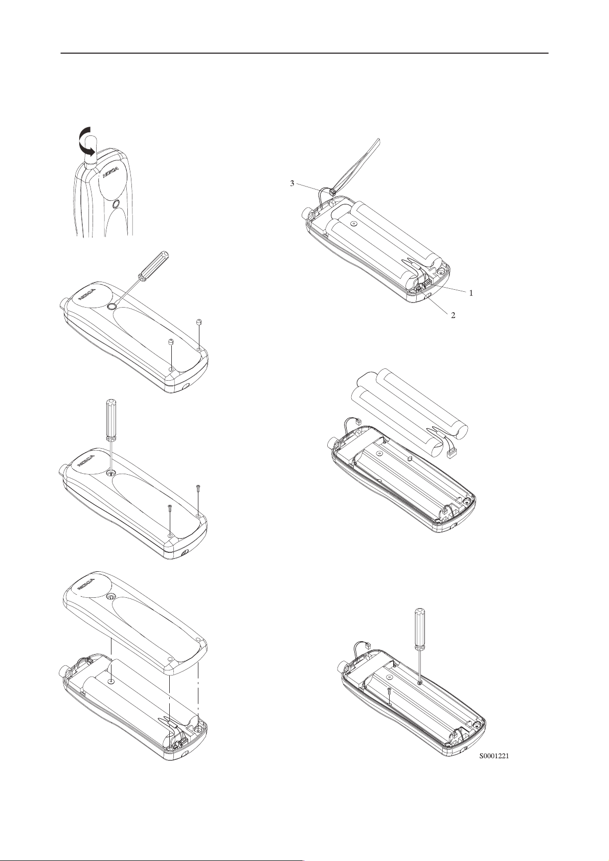
Disassembly instructions
1) Remove the
antenna
2) Remove screw
covers (3 pcs) with
screwdriver
Technical Documentation
5) Disconnect:
battery connector (1),
microphone connector (2),
and earphone connector (3)
with tweezers
3) Remove back
cover screws (3 pcs)
4) Remove
back cover
6) Remove
battery
7) Remove
chassis screws
Page 4
Original, 01/98
Page 5
PAMS
Disassembly & Troubleshooting Instructions
Technical Documentation
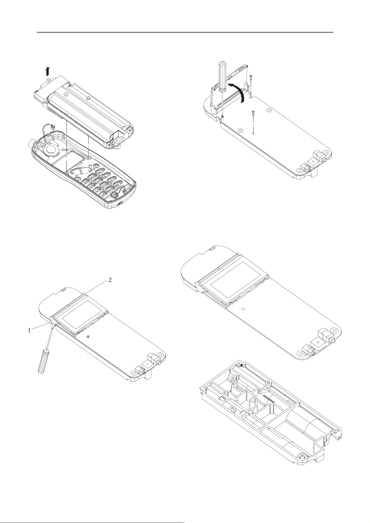
8) Remove
transceiver
module
NHX–4N
10) Lift display carefullly
Remove screws (3 pcs)
9) Turn around,
Loosen the light guide carefully
from both sides of the PCB with
flat headed tool
11) Chassis and module
can now be separated
Original, 01/98
Page 5
Page 6

Disassembly & Troubleshooting Instructions
PAMS
NHX–4N
General Trobleshooting
The object of troubleshooting is to define the faulty module block, and then to
locate the faulty component. The troubleshooting diagram has been planned so
that the fault, whatever it is, can be found as simply as possible.
The flow charts give you the overview of the blocks. The purpose is that you
proceed through the flow diagram so that, if your answer is YES for the asked
question, go straight to the next level, but if your answer is NO, go the subbranch.
Required servicing equipment:
– PC for Service Software
– Power supply (2.0A)
– Digital multimeter
– Oscilloscope
– Signal generator
– Spectrum analyzer
Technical Documentation
– RF cables
– Service cable SCN–3
– RF–adapter AAT–4X
– Test jig JBS–3N
– RS232/MBUS adapter
Page 6
Original, 01/98
Page 7

PAMS
Disassembly & Troubleshooting Instructions
Technical Documentation
General Troubleshooting
START
Will turn into
local mode ?
OK
Receiver OK ?
(SINAD OK)
The General troubleshooting chart shows
the most common fault areas These seven
fault types can be used to define the possible fault.
Logic fault
FAIL
Receiver fault
NHX–4N
OK
Transmitter operating
(RF power OK) ?
OK
Earphone level/
modulation
(nom, max)
OK
Is display/keypad
module working ?
OK
FAIL
FAIL
FAIL
Transmitter fault
Earphone level or
modulation fault
Display or keypad fault
Original, 01/98
END
OK
FAIL
Call set–up faultCall set–up ?
Page 7
Page 8

Disassembly & Troubleshooting Instructions
PAMS
NHX–4N
Logic fault
Logic fault
Power drops off or does
not assume local mode
OK
Check clock signal
of CLKMCU ~3.3 Vpp
FAIL
VL, VL2, VA and
VREF ~3.3 V or only
momentarily on
FAIL
Technical Documentation
Voltages always 3.3 V
FAIL
OK
XRES ~ 0 V
FAIL
OK
Check d.c. voltages
of N101;
– pin 17 ~1.75 V if
VBAT ~4.8 V
– pin 1, 5, 22 ~VBAT
Check;
– D201 pins 51 (CLKMCU), 21 and 53
(VL2), 67 and 68 (VREF), 12, 30,
50 and 58 (GND)
Check MBUS connection
d.c. voltages;
– D201/9 TXD ~3.3 V
– D201/10 RXD ~3.3 V
– X100/2 M2BUS ~3.3 V
Above lines are to show
to 3.3V all the time.
N101/14 XPWROFF line
at least 1 microsec. pulse to 3.3 V
3 sec. intervals (momentarily)
OK
OK
OK
FAIL FAIL
N101/13 PWRONX
line 0 V pulse (momentarily)
Check;
– solderings of MUUMI N101
– loading of supply voltages
– if OK, change N101
– Check load on VL2,
VA and VREF lines
Check;
– PWR button
– V930
– ROW0
– XPWROFF line (COL0) load
– If OK, change D201
Page 8
Original, 01/98
Page 9

PAMS
Disassembly & Troubleshooting Instructions
Technical Documentation
Receiver fault
Receiver fault
Simplex sens.
(TX off)
FAIL
See earphone level fault
N370/9 (DAF) OK?
OK
AF signal at
FAIL
VCCR, VREF,VSYN
OK?
FAIL
NHX–4N
Check: V310, V311
V313, V314,
N101/4
OK
TX spectrum
OK
Replace duplex
filter Z660
FAIL
Transmitter
fault
RX–VCO
oscillating
OK
VCO–freq
OK
FAIL
Check: operating voltage of
G530
Check: resistance through
N820/3, R521, R522, R523
FAIL
voltage N820/4,14
Connections of R530, C532
VCTCXO operating voltage
and frequency = 14.85 MHz.
Check SCLK, SDAT and SLE
lines.
OK
RXINJ
OK at V341
collector
FAIL
OK
at N370/16
FAIL
IF level
after Z350
FAIL
Check: solderings of
Z660, Z321, Z350
operation of V320
1. IF
OK?
OK
Check: voltage of N370/4,
components C378, R371,C377,
Z370, L370,
if OK replace N370
OK
Check operation
of V380
Check: RXINJ level at V341
collector (5–10 dBm), V341
operating voltage and bias, C341
Original, 01/98
Page 9
Page 10

Disassembly & Troubleshooting Instructions
PAMS
NHX–4N
Transmitter fault
Check: resistance through N820/17,R421, R422, R423
Transmitter fault
Transmitter
frequency
OK
OK
Connections of R430, C432.VCTCXO operating
voltage and freq. =14.85 MHz. Check SCLK,SDAT
and SLE lines.
FAIL
FAIL
TX–VCO
freq and spectrum
OK (TXE OFF)
OK
Technical Documentation
Buffer V430
output freq. and
spectrum OK
(TXE OFF)
OK
FAIL
Check: V430 operating
voltage and bias, C440
R440, C443
590<Pout<980 mW
(level High) at C642
OK
Check Z660 TX–pin
soldering. If OK replace
Z660
Check: R647, V642,R660
C643, VTSYN, TXE, TXC
R641, R655, R649, R640,
V650, V641, V640
FAIL
FAIL
Power OK after
tuning
FAIL
Vpc N601/1
2.5–3.5 V (level 1,2,3)
OK
TXINJ level
6–12 dBm after
Z601
FAIL
OK
OK
OK
Buffer V440
output freq. and
spectrum OK
(TXE ON)
OK
N601 freq.
and spectrum OK
when duplex filt.
not connected
FAIL
Check: C631, C641, C660
C642, C634, C635, C608
C625, C602. If Ok
replace N601.
FAIL
OK
Check: V440 operating
voltage and bias, C450,
R455, C454, TXE
Check soldering of duplex
filter Z660. If OK replace
filter.
Replace G430
Page 10
FAIL
VCO output
level –3...+3 dBm
OK
Check operation of V430
and V440
Original, 01/98
Page 11

PAMS
Disassembly & Troubleshooting Instructions
Technical Documentation
Audio fault
EARPHONE LEVEL / MODULATION LEVEL FAULT
SIGNAL LEVELS OF AUDIO CIRCUiT N701
MIC
PIN 46
XMIC
MICAM
50 mVrms
TXMUX+TXAAF
TXATT
MICTRI
ATTO
TXBP
ATTO
COMI
COMO
EMPI
EMPO
LPIN
COMI
PIN 47
PIN 49
PIN 50
PIN 51
PIN 52
PIN 53
COMPR
COMO
EMPI
50 mVrms
50 mVrms
70 mVrms
70 mVrms
95 mVrms
95 mVrms
EMPO LPIN
PREEM TXLP
LIM1 LIM2
TXTRI+TXPOSTFIL
WTRFIL+WPOSFIL
SUM
NHX–4N
MOD
PIN 55
170 mVrms
Signal levels are measured by oscilloscope and input signal frequency is 1 kHz. Transmitted signal deviation is 2.3 kHz.
HF CONTROL
VOL
RXTRI
PIN 27
DAF
125 mVrms
Signal levels are measured by oscilloscope. Received signal audio frequency is 1 kHz, deviation 5.7 kHz and power level –53dBm.
RXAAF EXP
RXMUX+AAFIL
DEEMP+RXFIL
FILOEXPI
EAMPBO
EXPO
VOLI
RXATT
EAR
ACC
FILO
EXPI
EAMPBO
EWCI PIN 31 100 mVrms
EXPO
VOLI
EARP
EARM
XEAR PIN 35 130 mVrms
PIN 28
PIN 29
PIN 30
PIN 32
PIN 34
PIN 38
PIN 37
EARP
EARM
EVGND
XEAR
180 mVrms
180 mVrms
100 mVrms
330 mVrms
330 mVrms
120 mVrms
120 mVrms
Original, 01/98
Page 11
Page 12

Disassembly & Troubleshooting Instructions
PAMS
NHX–4N
Display or keyboard fault
Display or keypad fault
FAIL
Lights OK ?
OK
KEYBOARD
FAULT
Display does’nt work
D201/29 LIGHTS
line at + V with
lights on
OK
Check operation of
switches V43 and V45
Pulses to 3.3V
on COL0–4 lines at
~50 ms intervals
FAIL
FAIL
Technical Documentation
Check load in lights line
(R920, R921, R922, R923, R924)
Check COL0–4 lines from
keyboard to D201
OK
Check pins
Pin 33 V5OUT ~–6.5 V
Pin 38 VCI ~3.3V
OK
Check pin
Pin 31 V5 ~–5.0V
OK
FAIL
FAIL
OK
ROW0–2 lines are to carry 3.3V
and pulses to 0 V at ~50 ms
intervals when corresponding
key depressed
clock signals
Pin 37 C1+ 3.3V/7.2kHz
Pin 35 C2+ 6.6V/7.2kHz
OK
Check soldered joints of D100
Check R901–904 and C902, C903
FAIL
Check components;
– C900, C901
Page 12
Check;
Display foil solder joints;
D100/40/LCDRES 3.3V
Original, 01/98
Page 13

PAMS
Disassembly & Troubleshooting Instructions
Technical Documentation
Call set–up fault
Call set–up fault
Phone will not
assume SERV – mode
Subscriber data OK ?
OK
OK
FAIL
NHX–4N
Check subscriber data and country codes and
correct them if needed.
RSSI operative ?
OK
Data
detection of N701
operative ?
OK
Replace N701
FAIL
FAIL
Check RSSI tunings and tune if needed.
Check N370/12/RSSI–line and the operation
Inspect the signal path from test point DAF
to N701/27
Check also other lines to N701.
Original, 01/98
D0000123
Page 13
Page 14

Disassembly & Troubleshooting Instructions
PAMS
NHX–4N
Technical Documentation
This page intentionally left blank.
Page 14
Original, 01/98
 Loading...