

Page 1

CCS Technical Documentation
RH-41 Series Transceivers
Troubleshooting Instructions
Issue 2 09/2003 Confidential Nokia Corporation
Page 2
RH-41
Troubleshooting Instructions CCS Technical Documentation
Page 2 Nokia Corporation Confidential Issue 2 09/2003
Page 3

RH-41
CCS Technical Documentation Troubleshooting Instructions
Contents
Page No
Transceiver Troubleshooting ......................................................................................... 5
Baseband Troubleshooting ..........................................................................................5
General testing........................................................................................................... 5
Troubleshooting ........................................................................................................ 5
Power up faults.......................................................................................................... 6
Flash Programming does not work.......................................................................... 10
Charging .................................................................................................................. 12
Audio failures.......................................................................................................... 13
Accessory detection................................................................................................. 16
Sleep Clock ............................................................................................................. 17
Display/Keyboard lights do not work ..................................................................... 18
Display does not work............................................................................................. 19
Buzzer does not work.............................................................................................. 20
Keyboard does not work ......................................................................................... 20
Receiver Troubleshooting ..........................................................................................20
General instructions for RX troubleshooting .......................................................... 20
Path of the received signal ...................................................................................... 20
Fault-finding charts for receiver chain .................................................................... 21
Transmitter Troubleshooting .....................................................................................26
General instructions for TX troubleshooting .......................................................... 26
Path of the transmitted signall................................................................................. 27
Fault-finding charts for the transmitter ................................................................... 27
Synthesizer Troubleshooting .....................................................................................33
19.44 MHz reference oscillator............................................................................... 33
RX VHF .................................................................................................................. 34
Fault-finding chart for RX VHF VCO ................................................................... 35
TX VHF................................................................................................................... 35
UHF Synthesizer ..................................................................................................... 36
Issue 2 09/2003 Nokia Corporation Confidential Page 3
Page 4

RH-41
Troubleshooting Instructions CCS Technical Documentation
Page 4 Nokia Corporation Confidential Issue 2 09/2003
Page 5
RH-41
CCS Technical Documentation Troubleshooting Instructions
Transceiver Troubleshooting
First, carry out a thorough visual check of the module. Make sure that:
• there are no mechanical damages
• the solder joints are OK
Note: Before changing anything, ALL SUPPLY VOLTAGES AND THE SYSTEM CLOCK / SLEEP
CLOCK should be checked.
Baseband Troubleshooting
General testing
The phone has three different modes for testing and/or repairing the phone. The modes
can be selected with suitable resistors connected to BSI- and BTEMP- lines as illustrated
in the following table:
Mode BSI-resistor BTEMP resistor Remarks
Local mode 0 - 1k 0 - 1k
Test mode >1k 0 - 1k
Normal mode 68k 47k Recommended for baseband
testing. Same as local mode, but
making a phone call is possible.
If the corresponding resistors are connected, the MCU software automatically enters into
the local or test mode when the supply voltage is connected to the phone.
The power can be switched on by:
1 Pressing the power key.
2 Connecting the local/test mode resistors to the bsi/btemp lines and connecting
the battery voltage to the phone.
3 Connecting a charger.
4 Phone’s internal functions (Real time clock alarm)
In the local and test mode, the baseband can be controlled through MBUS or FBUS (FBUS
is recommended) connections using Phoenix service software.
Troubleshooting
Note: Most of the baseband repair actions require removing the baseband shield. The shield must not
be removed unless separately authorized by the program.
Note: The phone’s ESN has to re-written to the UEM, if the UEM is replaced. This can be done only in
Central Service.
Issue 2 09/2003 Nokia Corporation Confidential Page 5
Page 6
RH-41
Troubleshooting Instructions CCS Technical Documentation
The BB troubleshooting instructions consist of the following topics:
1Power up
2 Flash programming
3Audio
• Earpiece
• Microphone
4 Charging
5 Accessory detection
6 Sleep clock
7 User interface
Power up faults
Power up sequence
1 The UEM acts as a HW master during start up
• Display
• Lights
• Buzzer
• Keyboard
• Vbatt limits: 2.1V for internal state machine, 3V triggering whole startup
• Regulator sequencing
• HW "core" regulators "on": Vio, Vcore, VR3, Vflash1
These regulators supply the processors, memory, chip interfaces and clock source in RF
• Reset releasing delay
• Supply voltages stabilize to their UEM HW default values
• RFCLK grows to full swing
• The core is ready to run but waiting for the PURX release
Page 6 Nokia Corporation Confidential Issue 2 09/2003
Page 7
RH-41
CCS Technical Documentation Troubleshooting Instructions
• Reset releasing
• The UPP releases the SLEEPX up to the "non sleep" -state to prevent the
UEM switching the regulators "OFF"
2 MCU starts running the Bootsrap Code
• Written in stone/ UPP internal ROM
• The program checks if there is any reason for the FDL mode (Flash Down Load)
• If there is an executable code in FLASH and there is no reason for FDL, the MCU
starts running the MCU program from FLASH.
3 MCU runs the FLASH MCU code
• The phone initialization, user interfaces, internal blocks etc.
• Core regulator voltage setting for required DSP speed
• Initializes the DSP and concerning HW
• Releases DSP reset -> DSP starts running
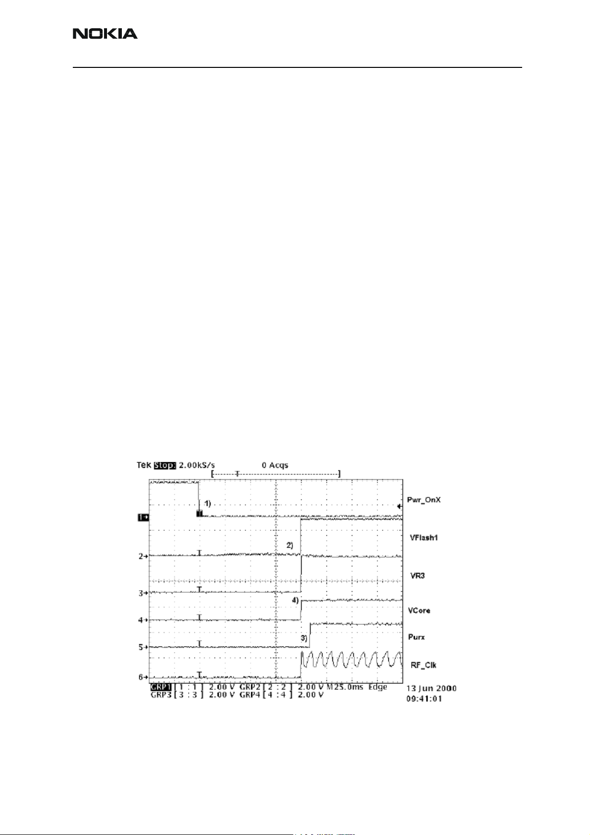
Note: In the following figure, the RF_Clk frequency appears to be lower than 19.44 MHz because of a
too low oscilloscope sampling frequency (2kS/s).
Figure 1: Power up sequence
Issue 2 09/2003 Nokia Corporation Confidential Page 7
Page 8

RH-41
Troubleshooting Instructions CCS Technical Documentation
1 Power key pressed
• After 20ms UEM enters RESET MODE if VBAT>Vmstr+
• VFLASH1, Vana, Vcore, Vio and VR3 goes high.
• VCTCXO enabled by VR3 -> RFClk 19.44 MHz running.
2Purx released
• Purx released by UEM, UEMINT goes high for 100 ms, SleepX goes high and
UEM starts feeding SleepClk (32 KHz) to UPP.
Note: The sleepclock starts running in the crystal circuitry (B200) immediately when the battery voltage is supplied.
3 Software running
• Default value for Vcore is 1.5 volts when the software is running.
• Cbus (1.08MHz) clock starts running.
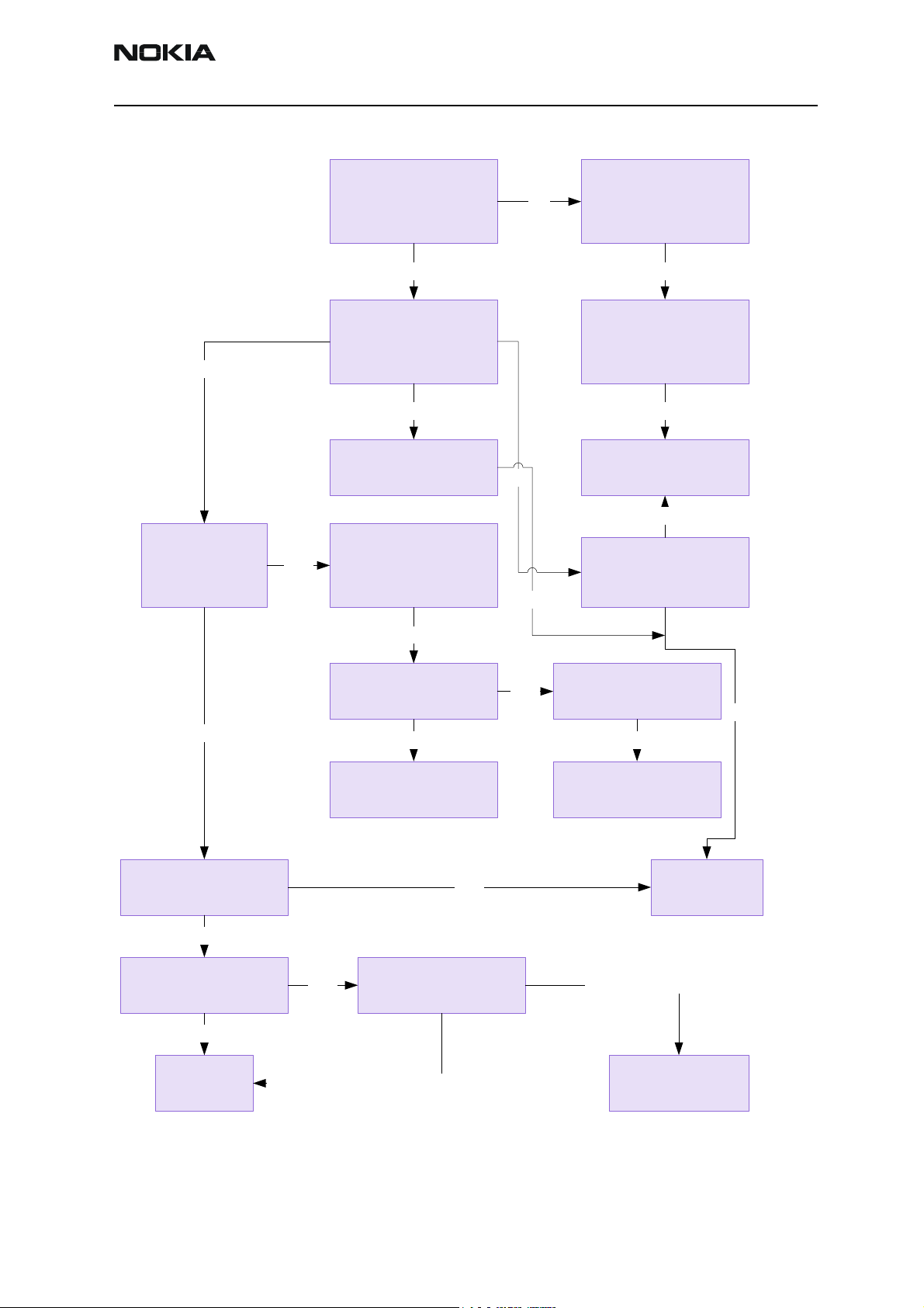
Phone does not start up normally or does not stay on
Note: In case of power up faults, it is not possible to force the phone on by disabling the watchdog.
Instead, measurements should be taken immediately when the power key is pressed or when the battery voltage is connected to the phone (local/test mode).
The easiest way to check if the software is running when the phone takes an abnormal
amount of current is to measure the cbusclk and Vcore.
The Dbus clock (programmable 9.72MHz) is not automatically visible in the test and local
modes.
Page 8 Nokia Corporation Confidential Issue 2 09/2003
Page 9
RH-41
CCS Technical Documentation Troubleshooting Instructions
OK
Check
19.44MHz RF
clock from C420
FAIL
Try to start phone to
test or local mode
FAIL
Measure Vflash1,
Vana, Vio, Vcore, VR3
when pwr key pressed
VANA and VR3 missing
Check G790 (missing
or misaligned)
Check C420
OK
FAIL
OK
OK
Check the power key
OK
R206, R207,
C220, C240
Check R202, R206,
R207, C220, C240
OK
Check X101
FAIL
Measure VBAT from
C261
OK
Check that purx goes
up to 1.8V
OK
Measure J406 (it
should be 1.08MHz)
OK
Change
UPP (D400)
Check 19.44MHz from
G790
FAIL
FAIL
Programming OK but phone doesn't start
Reflash phone
FAIL
Check R792, C792,
C793
OKOK
Change G790Change N801
Change UEM
(D200)
Programming fails
Go to Flash
Failure flowchart
OK
Figure 2: Fault tree, phone does not power up
Issue 2 09/2003 Nokia Corporation Confidential Page 9
Page 10
RH-41
Troubleshooting Instructions CCS Technical Documentation
Flash Programming does not work
Flash programming procedure
1 The phone communicates with the prommer via the production test pattern,
using the following signals:
• FBUSTX(serial data to phone)
• FBUSRX(serial data from phone)
• MBUS(serial clock for FBUSRX)
• VPP(External flashing voltage for speed up flashing)
The BSI line is also used when initializing flashing (battery connector).
2 When the phone is powered (VBAT>3V), the MBUS and FBUSTX lines are pulled
up internally by the phone.
3 The prommer sends a command to the UEM, using FBUSRX, to enter the Flash
mode. During the sending of this command, the prommer keeps the BSI line high
and MBUS is used as a serial clock.
4 When the Flash mode command is acknowledged, UEM enters the Flash mode
and releases reset (PURX) to MCU.
5 After reset is released, UPP checks if there is a request for the Bootstrap code
(that resides in the UPP ROM).
6 The request for Bootstrap is the MBUS pulled down by the prommer (if the boot-
strap is not requested, the bootstrap code jumps to FLASH SW).
7 If the Bootstrap code is requested, UPP enters the Flash mode and sets FbusTX to
'0' as an acknowledgement to the prommer. This is an indication that UPP can
run, at least, the fixed Bootstrap code – although it is not able to run the FLASH
code. UPP then sends an UPP-ID to the prommer via the FBUSTX line.
8 After the prommer has received the UPP ID, it sends a corresponding Secondary
Boot Code to the phone via FBUSRX. The Secondary Boot Code, when run in UPP,
requests UPP to send information to the prommer about the flash type and other
HW-related parameters about the device to be flashed.
9 Prommer then sends the Algorithm Code corresponding to the HW parameters,
and this algorithm, when run in UPP, takes over handling the MCUSW transfer to
Flash.
10 12 volts can be supplied to Vpp (by the prommer) to speed up flashing.
Page 10 Nokia Corporation Confidential Issue 2 09/2003
Page 11
RH-41
CCS Technical Documentation Troubleshooting Instructions
11 The FLASH Program includes a package of MCU and DSP software and all default
parameters for the phone. The tuning values will be added/rewritten during the
Flash/Alignment phase.
Flash programming error codes
The various error codes can be seen from the FPS-8 Flash in Phoenix.
The underlined text in the following table indicates that the item under consideration is
being used for the first time in the flashing sequence.
Error Description Not working properly
C101 "The Phone does not set FbusTx line high
after the startup."
C102 "The Phone does not set FbusTx line low
after the line has been high. The Prommer
generates this error also when the Phone is
not connected to the Prommer."
C103 "Boot serial line fail." Mbus from Prommer->UEM->UPP(MbusRx)(SA0)
C104 "MCU ID message sending failed in the
Phone."
C105 "The Phone has not received Secondary boot
codes length bytes correctly."
C106 "The Phone has not received Secondary code
bytes correctly."
Vbatt
Vflash1
Vcore
VIO
BSI and FbusRX from prommer to UEM.
FbusTx from UPP->UEM->Prommer(SA0)
PURX(also to Taco)
VR3
Rfclock(VCTCXO->Taco->UPP)
Mbus from Prommer->UEM->UPP(MbusRx)(SA1)
FbusTx from UPP->UEM->Prommer(SA1)
FbusRx from Prommer->UEM->UPP
FbusTx from UPP->UEM->Prommer
FbusTx from UPP->UEM->Prommer
Mbus from Prommer->UEM->UPP(MbusRx)
FbusRx from Prommer->UEM->UPP
FbusTx from UPP->UEM->Prommer
Mbus from Prommer->UEM->UPP(MbusRx)
FbusRx from Prommer->UEM->UPP
FbusTx from UPP->UEM->Prommer
C107 "The Phone MCU can not start Secondary
code correctly."
A204 "The flash manufacturer and device IDs in
the existing Algorithm files do not match
with the IDs received from the target
phone."
A387 "The MCU ID in the MCUSW.” UPP
C601 "The prommer has detected that Vpp voltage
level has dropped below the limit"
UPP
Flash
Signals between UPP-Flash
Vpp from prommer - >Flash
Issue 2 09/2003 Nokia Corporation Confidential Page 11
Page 12

RH-41
Troubleshooting Instructions CCS Technical Documentation
C383
C583
C683
C384
C584
C684
C585
C685
C586
C686
Charging
Note: The charging voltage and current can be checked by connecting the phone to the service software and reading the ad- converter values of the vchar and ichar.
"The Prommer has not received Phone
acknowledge to the message."
(C383-during algorithm download to target
phone)
(C583-during erasing)
(C683-during programming)
"The Phone has generated NAK signal during
data block transfer."
(C384-during algorithm download to target
phone)
(C584-during erasing)
(C684-during programming)
Data block handling timeout"
(C585-during erasing)
(C685-during programming)
"The status response from the Phone informs
about fail."
(C586-during erasing)
(C686-during programming)
Flash
UPP
Signals between UPP-Flash
Flash
UPP
Signals between UPP-Flash
Flash
UPP
Signals between UPP-Flash
Flash
If charging fails when the LCH-9 is used, and works with ACP-7 and ACP-8, check that
the charge control pin of the system connector is connected to the ground.
Page 12 Nokia Corporation Confidential Issue 2 09/2003
Page 13

RH-41
CCS Technical Documentation Troubleshooting Instructions
Phone doesn't
start charging
Connect charger and
check VCHARIN
OK
Check ICHAR
Fail
Check R202, R206,
R207, C201, C202,
C220, C240, and
R200
OK
Fail
Check F100, L100,
V100, and C106
OK
Check bottom
connector
-VIN
_Charge control pin
Change the UEM
Figure 3: Fault tree, charging
Audio failures
In case of audio failures, there are three possibilities to check the audio lines.
1 Make a phone call against tester and check audios.
2 In case the earpiece/XMIC fails: Feed a 1 Khz signal to the XMIC line and measure
the signal from the earpiece line. The Audio test box (JBA-8) is needed. The Audio
loop (Audio test/Ext In Hp Out) must be switched on by the Phoenix service software. This loop will connect audios only through the UEM. In this case, the UPP is
not used.
In case the internal microphone/XEAR fails: Feed the tone to the microphone and measure the signal from the XEAR line. The Audio test box (JBA-8) is needed. The Audio loop
Issue 2 09/2003 Nokia Corporation Confidential Page 13
Page 14

RH-41
Troubleshooting Instructions CCS Technical Documentation
(Audio test/Hp In Ext Out) must be switched on by the Phoenix service software. This loop
will connect audios only through the UEM. In this case, the UPP is not used.
3 Run the audio-loop self-test with Phoenix (BB Self Tests/
ST_EAR_DATA_LOOP_TEST). This loop will test the ear-data/mic-data lines
between the UPP and the UEM.
Earpiece or external microphone line does not work
Earpiece
doesn't work
Feed 1KHz to XMIC
R un audio loop self-
tes t with P hoenix
Fail
by J BA-8 and
measure from
earpiece
OK
Check R 157
OK
Check earpiece
OK
Change UEM
OK
Fail
Change UPP
Figure 4: Fault tree, earpiece failure
Page 14 Nokia Corporation Confidential Issue 2 09/2003
Page 15

RH-41
CCS Technical Documentation Troubleshooting Instructions
Microphone or XEAR line does not work
Microphone does n't
work
R un audio loop self-
tes t with P hoenix
OK
Check R 156, C151,
C152, C 157, L164
OK
Check microphone
Fail
Feed 1KHz to MIC by
J B A-8 and measure
from XE AR
OK
Fail
Change UPP
Change UEM
Figure 5: Fault tree, microphone failure
Issue 2 09/2003 Nokia Corporation Confidential Page 15
Page 16

RH-41
Troubleshooting Instructions CCS Technical Documentation
Accessory detection
1 Start the phone in the normal mode when checking for accessory detection.
2 The Ad- converter value of the hookint-line can be checked with the Xmic-
switch on an MJS-18 test jig. Changes normally from high to low when no accessory is connected.
3 When the headset (HDC-5) is connected, the hookint- value should be between
600 and 800.
Accessory detection
doesn't work normally
Check Headint ad
value with Phoenix
(no accessory
connected
- Headint ~0 *)
Fail
Check R151 and
C160
OK
Check bottom
connector
OK
OK
Use XMIC switch on
MJS-18 and check
hookint ad value.
Should go from high
(~1000) to low (~0)
OK
Fail
Check R152, C161,
L160
OK
Check R150, R201,
C104, C106, L162,
L163
OK
* On local or test
Change UEM
Figure 6: Fault tree, accessory detection
mode Headint <400
Page 16 Nokia Corporation Confidential Issue 2 09/2003
Page 17

RH-41
CCS Technical Documentation Troubleshooting Instructions
Sleep Clock
Missing/nonfunctional sleep clock causes
• Entering sleep mode fails (higher current consumption -> shorter standby
time).
• Baseband self tests cannot be run.
• Phone clock (on display) does not function properly.
Sleep mode not
working
Measure sleep clock
Measure sleep clock
Fail Fail
Figure 7: Fault tree, sleep clock
from B200
Check C209 and
C210
OKOKOK
Change B200Change UEM (D200)Change UPP (D400)
Issue 2 09/2003 Nokia Corporation Confidential Page 17
Page 18

RH-41
Troubleshooting Instructions CCS Technical Documentation
Display/Keyboard lights do not work
Display/K eyboard
lights are not
working
Check R 300
(Display) and R301
(K eyboard)
OK
Fail
Replace resistor(s)
Check LEDs
V300...V303 (Dis play)
and V304...V309
(K eyboard)
OK
Use Display Test in
Phoenix to set lights
ON/OFF
Figure 8: Fault tree, Display/Keyboard lights
Fail
Fail
Replace LED(s)
Replace UEM
Page 18 Nokia Corporation Confidential Issue 2 09/2003
Page 19

RH-41
CCS Technical Documentation Troubleshooting Instructions
Display does not work
Display does not
work
Check that phone
powers up normally
(current
cons umption, power
up sequence)
Fail
Proceed to Phone
Doesn't Power Up
troubleshooting
OK
Check display
visually (possible
cracks on COG
driver or glass ,
capacitors loose or
broken)
OK
Check PWB and
elastomer connector
OK
R un L C D test in
Phoenix (BB Self
Tests/
S T_LCD_TES T)
OK
Fail
Replace Display
Module
Clean PWB and
Fail
replace elas tomer if
needed.
Fail Fail
Check capacitors
C302...C304
OK
In any phase of Display
troubleshooting, use
Display Test in Phoenix to
produce test patterns on
display.
Also check with a known
good dis play module to
see if it works .
R eplace capac itor(s )
Use Display Test in
Phoenix to check if
display works
Fail
R eplace elas tomer
Fail
Replace Display
Module
Replace Display
Module
Figure 9: Fault tree, Display does not work
Issue 2 09/2003 Nokia Corporation Confidential Page 19
Page 20

RH-41
Troubleshooting Instructions CCS Technical Documentation
Buzzer does not work
Check spring connectors and C306.
• No sound: Try using a known good buzzer instead. If there is still no sound, change the
UEM (D200)
• Weak sound: Use the Audio test in Phoenix to set the buzzer parameters (frequency,
strength). If it does not affect the sound level, change the buzzer.
Keyboard does not work
Check that there is no dirt between the dome sheet and the PWB. Check EMI/ESD filter
(Z301) that all lines come through. If not, change Z301. If the keyboard still does not
operate normally, try to use the Keyboard test in Phoenix to see if the pressed key is
identified. If it is not identified, change the UPP (D400).
Receiver Troubleshooting
General instructions for RX troubleshooting
Start the Phoenix software and use it to start the required RX mode of the mobile phone.
The troubleshooting flowchart is divided into three steps: (1) general checking, (2) local
checking, and (3) RX chain checking.
Note: Before changing ASICs or filters, all solderings and missing components must be checked visually. After any possible component changes, the phone must be tuned with the Phoenix autotune SW.
Path of the received signal
Block level description of the receiver:
(Antenna/ext RF) – Diplexer – Duplexer – Low Noise Amplifier (LNA) – RX band filter –
First mixer – 135.54 MHz RX IF filter – IF-amplifier – second mixer – 14 kHz low-pass filter – adjustable IQ amplifier – Baseband.
Page 20 Nokia Corporation Confidential Issue 2 09/2003
Page 21

RH-41
CCS Technical Documentation Troubleshooting Instructions
Fault-finding charts for receiver chain
AMPS
Apply 881.49MHz = ch
383 -116dBm, 8kHz
dev, 1 kHz sine to
external RF connector
X900
Y
Connect HS to cellular
tester. Open AF: 1kHz
sine meas SINAD
AF:>12 dB
Y
AMPS RX chain OK
N
Check UHF Vc (from
C773) V: 1.8...2.1V
Y
Check RXVHF Vc
(from C740).
V:0.7...1.3
Y
Apply 881.49 MHz
-30dBm sine signal to
external RF connector
X900
N
N
Start troubleshooting
Start troubleshooting
Issue 2 09/2003 Nokia Corporation Confidential Page 21
Page 22

RH-41
Troubleshooting Instructions CCS Technical Documentation
Note! Check all
Check input level at
diplexer (Z907) input
Y
N
Change EXT RF
connector
soldering and
components in
antenna circuit
before changing.
Check input level at
duplex filter (Z906)
Y
.
Check input level at
LNA input (N801 pin
N14)
Y
Check RF level at
RX800 band filter
input (Z820)
MIX1Ain P/N.
N
N
Change diplexer
Change duplex filter
Change RX800 Band
N
(Z907)
(Z906)
Taco
Filter
(Z820)
Taco
Z907
Note! Check all
soldering and
discrete
components of front
end.
Taco
Note! Check all
soldering and
discrete
components around
Taco before
changing.
Y
Check RF level at
MIX1Ain P/N
Y
N
Change Taco (N801)
Page 22 Nokia Corporation Confidential Issue 2 09/2003
Page 23

RH-41
CCS Technical Documentation Troubleshooting Instructions
Check RF level at RX
IF filter input at
135.54MHz (Z830)
Y
Check RF level at RX
IF filter output at
135.54MHz
Check RF level at
N N
J751 and J752 at
2034.06MHz
Y
Change Taco (N801)
N
Change RX IF filter
Taco
(Z830)
Start synthesizer
troubleshooting
Note! Check all
discrete
components and
voltages around
Taco.
Y
Check RX I and Q
signals at I: J801(+),
J803(-) and Q:
J804(+), J802(-)
Y
Check UEM and start
baseband
troubleshooting
Check RF level by
N N
L730 without having
electrical contact at
271.08MHz
Y
Taco
Change Taco (N801)
Start synthesizer
troubleshooting
Figure 10: Fault tree. AMPS
Issue 2 09/2003 Nokia Corporation Confidential Page 23
Page 24

RH-41
Troubleshooting Instructions CCS Technical Documentation
TDMA800
Since the same physical signal path is used for both analog and digital modes at the
lower band, there is no need for additional troubleshooting in the digital mode. So if the
digital mode at the lower band is not working properly, start the analog mode troubleshooting.
TDMA1900 (dual band)
Only EXT RF connector -> 1st IF needs separate troubleshooting at upper band. After
down conversion (RF -> 135.54 MHz) both lower and upper band use same signal path.
Apply 1960.02MHz =
ch 1000 -110dBm
signal to external RF
connector X900
Y
Enable loopback BER
using RF test UI and
check sensitivity: -110
dBm BER < 3%
N
Check UHF Vc (from
C773) V:2.2...2.6V
Note! These tests
are done in local
mode by using RF
test UI
Y
N
TDMA1900 RX chain
is OK
Start synthesizer
troubleshooting
Y
Check RXVHF Vc
(from C740),
V:0.7...1.3
Y
N
Start synthesizer
troubleshooting
Page 24 Nokia Corporation Confidential Issue 2 09/2003
Page 25

RH-41
CCS Technical Documentation Troubleshooting Instructions
Note! Check all
Check input level of
diplexer (Z907)
Y
Check input level of
duplex filter (Z962)
N
N
Change EXT RF
connector
Change diplexer
(Z907)
soldering and
components in
antenna circuit before
changing.
Note! Check all
soldering and
discrete components
of front end.
Y
Check RF level at
LNA input (at duplex
filter RX output port)
Y
Check RF level at
RX1900 band filter
(Z850) input
Y
Taco
Note! Before
N
Change duplex filter
(Z962)
replacing Taco, check
all solderings and
components around
V850.
Taco
Check voltage at
N
C854 out (V850 in),
Change Taco (N801)
V: about 2.7V
Issue 2 09/2003 Nokia Corporation Confidential Page 25
Page 26

RH-41
Troubleshooting Instructions CCS Technical Documentation
Y
Check RF level at
MIX1_B input
Y
Check RF level at RX
IF filter input at
135.54MHz
Y Y
Continue
troubleshooting like
LB
N
N N
Change RX1900 band
filter
Check RF level at
J751 and J752 at
2095.56MHz
Taco
Change Taco (N801)
Start synthesizer
troubleshooting
Note! Check all
discrete
components and
voltages around
Taco.
Figure 11: Fault tree: TDMA 1900 troubleshooting
Transmitter Troubleshooting
General instructions for TX troubleshooting
Always use an RF cable connected from an external RF connector to the analyzer via (rfpower) attennuator. This is important to protect the analyzer against excessive RF power
and not to allow leakage of undesired RF power into the cellular frequencies.
1 Start the Phoenix software and select the TX mode under Testing (AMPS,
DAMPS).
2 It is useful to select the mid channel (383 for AMPS/DAMPS) and the power
level 2.
Note: After any component change, tune the phone with the Phoenix autotune SW.
Page 26 Nokia Corporation Confidential Issue 2 09/2003
Page 27

RH-41
CCS Technical Documentation Troubleshooting Instructions
Path of the transmitted signal
l
AMPS/DAMPS
UEM TX I/Q DA-converters -> I/Q modulator and Digital gain step amplifier (Taco) ->
IF-BPF -> Upconverter+driver (Taco) -> Balun->BPF -> PA -> Coupler (Power detector)
-> Duplex-filter -> Diplexer -> EXT RF-connector -> Antenna
TDMA 1900 (dual band)
UEM TX I/Q DA-converters -> I/Q modulator and digital gain step amplifier (Taco) -> IF
BPF -> Upconverter+driver (Taco) -> Balun -> BPF -> PA -> Coupler (power detector)
-> Duplex-filter -> Diplexer -> EXT RF connector -> Antenna
Fault-finding charts for the transmitter
AMPS
1 Start the Phoenix software and set the phone to the analog mode by using RF
Test UI.
2 Set the channel to 383 and the power level to 2.
3 Connect the RF cable to the Ext RF connector.
4 Connect the cable to the Spectrum analyzer input.
5 Measure the RF level.
Note: Insertion loss of the cable and attenuations.
Issue 2 09/2003 Nokia Corporation Confidential Page 27
Page 28

RH-41
T
Check Z960 i
f
T961
B
Troubleshooting Instructions CCS Technical Documentation
AMPS, PL2, CH383
Visual check of TX
-PA
-TX SAW
-Duplex filter
-Passive components
-PA
OK
Start synthesizer
troubleshooting
OK
Check supply voltage
-VR2
-VBATTRF
-VR5
-IPA1
OK
Check TXi/q signals
test points J901...J904
OK
nput and
Check Z960 input and
output power
output power
out:-20dBm+3/-6dB
out:-20dBm+3/-6dB
IL:2dB
IL:2dB
NOK
NOK
NOK
Check UEM and UPP
(baseband)
Check UEM
(baseband)
Taco
Change Taco or Z960
or Z960
OK
Check TX RF
rom balun
(836.49MHz) output
input RF:0dBm+/-6d
power from balun
NOK
aco
Change Taco
T961 input RF:
0dBm+/-6dB
OK
Page 28 Nokia Corporation Confidential Issue 2 09/2003
Page 29

RH-41
CCS Technical Documentation Troubleshooting Instructions
Check TX SAW input
and output power
IL:-3dB
OK
Is ltot 700...900 mA?
Check PA output
power and gain.
Output power:
~28dBm
Gain: ~30dB
OK
Check PWRDET
(N930) insertion loss
IL<0.3dB
OK
NOK
NOK
NOK
Change TX SAW filter
(Z905) or (T961)
or T961
Change PA (N901)
Change PWRDET
(N930)
Check duplexer (Z906),
diplexer (Z907) and RF
connector (X900)
insertion loss.
Dupl IL ~2.2dB
Dipl ~0.35dB
RF conn ~0.1dB
OK
Start power control
troubleshooting
Figure 12: Fault tree. Transmitter troubleshooting
NOK
Change Z906 or Z907
or RF connector
Issue 2 09/2003 Nokia Corporation Confidential Page 29
Page 30

RH-41
Troubleshooting Instructions CCS Technical Documentation
TDMA800
The transmitter chain is exactly the same as the AMPS mode, except for the IPA current.
TDMA 1900 (dual band)
TDMA 1900 mode and DAMPS mode have a common RF modulator and thus it is important that the DAMPS mode have no faults.
TDMA 1900, PL2, CH1000
Is TDMA800 mode
OK?
OK
Check LO signal
(2079.78MHz)@T775
and TX VHF
(363.6MHz)@N750
OK
Check supply voltage
-VR2
-VBATTRF
-VR6
-IPA2
-TXP2
OK
Check TX IF input
power
(181.80MHz)@Z960
IF: -20dBm+3/-6dB
NOK
NOK
NOK
NOK
Start AMPS
troubleshooting
Start synthesizer
troubleshooting
Check UEM and UPP
(baseband)
Change Taco or Z960
Taco
OK
Check TX RF
(1879.98MHz) output
power @T960 input
RF: 0dBm+/-6dB
OK
NOK
Change Taco
Taco
Check Z961 input and
output power
NOK
Change Z961
IL:-3dB
OK
Page 30 Nokia Corporation Confidential Issue 2 09/2003
Page 31

RH-41
CCS Technical Documentation Troubleshooting Instructions
Is ltot 350...450 mA?
Check PA output
power and gain.
Output power:
~29dBm
Gain: ~30dB
OK
NOK
Change PA (N960)
Check PWRDET
(N930) insertion loss
IL<0.3dB
OK
Check duplexer
(Z906), diplexer
(Z907) and RF
connector (X900)
insertion loss
Dupl IL ~2.2dB
Dipl ~0.35dB
RF conn ~0.1dB
OK
Start power control
troubleshooting
NOK
NOK
Change PWRDET
(N930)
Change Z906 or Z907
or RF connector
Figure 13: TDMA 1900 troubleshooting
Issue 2 09/2003 Nokia Corporation Confidential Page 31
Page 32

RH-41
Troubleshooting Instructions CCS Technical Documentation
Power control loop
Basically, the power detection is done with the Power detector module and power control is done inside the Taco. Power detection is basically similar for both bands, except
that both bands have their own coupler.
Is PWRDET vs output
power OK?
See chart below.
Y
Is DAC value vs.
PWRDET (mV) OK?
N
N
Figure 14: Fault tree: Power control loop
Check VR2 and
RFTEMP. Check
C930, C931, and
PWRDET module.
Check UEM
(baseband)
Note! See PWRDET vs
Output power curve
The detected voltages are illustrated in the following table and diagram:
800A 800D 1900D
Pout TXPWRDET Pout TXPWRDET Pout TXPWRDET
PL dBm dac mV dBm dac Mv dBm dac mV
2 24.8 712 1984 27.3 779 2201 27.3 702 1980
3 21.6 512 1437 23.3 476 1312 23.3 431 1198
4 18.5 340 961 19.3 284 759 19.3 262 730
5 14.5 239 686 15.3 171 462 15.3 158 445
6 10.5 180 510 11.3 98 271 11.3 88 253
7 6.5 141 415 7.3 56 151 7.3 50 148
8---3.330843.32679
9 - - - -0.7 14 46 -0.7 14 44
§0----4.75 16 -4.76 20
Note: DAC values may vary about +- 20%
Note: TXPWRDET is the difference between TX on burst and off burst.
Page 32 Nokia Corporation Confidential Issue 2 09/2003
Page 33

RH-41
CCS Technical Documentation Troubleshooting Instructions
2500
2000
1500
A800
1000
Voltage [mV]
500
0
2345 678 91
Power Level
D800
Synthesizer Troubleshooting
There are four oscillators generating the needed frequencies for RF section: 19.44 MHz
VCTCXO is used as a reference signal oscillator reference oscillator, 2 GHz UHF VCO with
loop filter circuit is used for RX and TX channel selection, TX VHF and RF VHF are for TX
modulator, and 2nd RX mixer locals generation.
The VHF synthesizers are integrated in Taco, but have external VCO coils and loop filters.
RX VHF frequency is fixed 271.08 MHz and TX VHF is fixed to 271.08 MHz . All locals are
locked to stable 19.44 MHz reference oscillator.
The frequency range for 2 GHz UHF VCO is: 2009.1 MHz … 2125.53 MHz. The output frequency range for the lower band is from 2009.16 MHz to 2059.02 MHz. In upper band,
the output frequency range from the UHF VCO is from 2031.78 MHz to 2125.53 MHz.
It is practical way to check out synthesizer status by measuring control voltage of the
VCO from Integrator capacitor. If voltage is stable and reasonable, local oscillators are
running correctly.
19.44 MHz reference oscillator
The VCTCXO oscillator frequency (G790) is controlled by UEM. This output 19.44 MHz
signal is connected to Taco. It is used as a reference signal in Taco and also fed out as
buffered clock signal to UPP. All synthesizers use divided 19.44 MHz signal as a reference
signal for Phase locked loop to provide correct LO frequency.
Figure 15: Detected voltage limits
Issue 2 09/2003 Nokia Corporation Confidential Page 33
Page 34

RH-41
Troubleshooting Instructions CCS Technical Documentation
START HERE!
2. Change VCTCXO
OK
2. No
Is VCTCXO
oscillating? 19.44MHz
1. No OK
1. Check voltage at
C792
2.78V
OK!
RX VHF
No OK
Check resistor R792
Figure 16: Fault tree: 19.44 MHz oscillator
The RX VHF signal is used to generate receiver Intermediate frequency. RX VHF has one
fixed frequency 271.08 MHz. Operating frequency is locked in Phase locked Loop.
RX VHF PLL output signal is integrated in Taco. There are only four external components:
VCO coil (L730), and loop filter components C740, C741, and R741.
Page 34 Nokia Corporation Confidential Issue 2 09/2003
Page 35

RH-41
CCS Technical Documentation Troubleshooting Instructions
Fault-finding chart for RX VHF VCO
1. START HERE
3. Replace Taco
OK Yes
2. No
Is frequency locked to
271.08MHz?
OK
TX VHF
1. No
2. Check resonator
1
components:
L730, C740, C741,
R741
Figure 17: Fault tree: RX VHF
OK
The TX VHF signal is used to generate transmitter Intermediate frequency. TX VHF VCO
has one fixed frequency (361.08). Operating frequency is locked in Phase locked loop. TX
VHF VCO output signal is divided by 2 and fed to the modulator.
1. START HERE
3. Replace Taco
Is frequency locked to
361.08MHz?
YesOK
OK
2. No
1. No
2. Check resonator
components:
L746, C720, C721,
R721
Figure 18: Fault tree: TX VHF
OK
Issue 2 09/2003 Nokia Corporation Confidential Page 35
Page 36

RH-41
Troubleshooting Instructions CCS Technical Documentation
UHF Synthesizer
The UHF VCO signal is used for RF channel selection. This signal is fed as a local signal for
1st mixer of RX path and for upconverter of TX path. When operating on lower band the
VCO signal is divided by 2 before feeding. This synthesizer is used for channel selection in
all modes and both bands.
The UHF synthesizer consists of an external 2GHz VCO module with loop filter components and integrated PLL parts in Taco. Integrated charge pump circuit allows analog and
digital operation modes. The VCO Oscillation frequency is from 2009.1 MHz to
2125.53 MHz. The output frequency of the VCO module depends on the DC control voltage which is controlled by PLL circuit inside Taco.
Change VCO
3. No
. No
OK
Check loopfilter
components
and balun
OK
START HERE
Is frequency locked to
2034.06MHz?
1. No OK
Yes
4. No
Is EVM OK?
1. No OK
Check loopfilter
components
Yes
Change
Taco
2. No
OK
OK
Check VCO operating
voltage:
2.78V
No
Figure 19: Fault tree: UHF Synthesizer
Check resistor R774
Page 36 Nokia Corporation Confidential Issue 2 09/2003
 Loading...