

Page 1

CCS Technical Documentation
RH-41 Series Transceivers
System Module
Issue 2 09/2003 Confidential Nokia Corporation
Page 2

RH-41
System Module CCS Technical Documentation
Page 2 Nokia Corporation Confidential Issue 2 09/2003
Page 3

RH-41
CCS Technical Documentation System Module
Contents
Page No
Abbreviations ................................................................................................................. 7
Transceiver RH-41 (Nokia 2260) .................................................................................. 9
Introduction ..................................................................................................................9
Operational Modes .................................................................................................. 10
Environmental Specifications ....................................................................................10
Normal and extreme voltages.................................................................................. 10
Temperature Conditions.......................................................................................... 10
Engine Module............................................................................................................. 11
Baseband Module ......................................................................................................11
UEM ..........................................................................................................................12
Introduction to UEM ............................................................................................... 12
Regulators................................................................................................................ 12
RF Interface............................................................................................................. 13
Charging Control..................................................................................................... 13
Digital Interface....................................................................................................... 13
Audio Codec............................................................................................................ 14
UI Drivers................................................................................................................ 14
AD Converters......................................................................................................... 14
UPP ............................................................................................................................14
Introduction ............................................................................................................. 14
Blocks...................................................................................................................... 14
Flash Memory ............................................................................................................15
Introduction ............................................................................................................. 15
User Interface Hardware .............................................................................................. 15
LCD ...........................................................................................................................15
Introduction ............................................................................................................. 15
Interface................................................................................................................... 15
Keyboard ....................................................................................................................15
Introduction ............................................................................................................. 15
Power Key ............................................................................................................... 16
Keys......................................................................................................................... 16
Lights .........................................................................................................................17
Introduction ............................................................................................................. 17
Interfaces ................................................................................................................. 17
Technical Information ............................................................................................. 17
Audio HW .................................................................................................................... 17
Earpiece .....................................................................................................................17
Introduction ............................................................................................................. 17
Microphone ................................................................................................................17
Introduction ............................................................................................................. 17
Buzzer ........................................................................................................................17
Introduction ............................................................................................................. 17
Battery.......................................................................................................................... 18
Phone Battery .............................................................................................................18
Introduction ............................................................................................................. 18
Interface................................................................................................................... 18
Battery Connector ......................................................................................................19
Issue 2 09/2003 Nokia Corporation Confidential Page 3
Page 4

RH-41
System Module CCS Technical Documentation
Battery Connector Interface .......................................................................................19
Accessories Interface ................................................................................................... 19
System connector ......................................................................................................... 19
Introduction ............................................................................................................. 19
Interface................................................................................................................... 19
Technical Information ............................................................................................. 21
PPH-1 Handsfree .......................................................................................................21
Introduction ............................................................................................................. 21
Interface................................................................................................................... 21
Charger IF ..................................................................................................................21
Introduction ............................................................................................................. 21
Interface................................................................................................................... 21
Test Interfaces .............................................................................................................. 22
Production Test Pattern ..............................................................................................22
Other Test Points .......................................................................................................22
EMC ............................................................................................................................. 23
General .......................................................................................................................23
BB Component and Control IO Line Protection .......................................................23
Keyboard lines......................................................................................................... 23
C-Cover ................................................................................................................... 23
PWB ........................................................................................................................ 23
LCD......................................................................................................................... 23
Microphone ............................................................................................................. 23
EARP....................................................................................................................... 23
Buzzer...................................................................................................................... 23
System Connector Lines.......................................................................................... 24
Battery Connector Lines.......................................................................................... 24
MBUS and FBUS.................................................................................................... 24
Transceiver Interfaces .................................................................................................. 24
BB - RF Interface Connections .................................................................................24
BB Internal Connections ............................................................................................28
UPP Block Signals .....................................................................................................33
Memory Block Interfaces ..........................................................................................37
Audio Interfaces .........................................................................................................38
Key/Display blocks ....................................................................................................40
Keyboard Interface.................................................................................................. 40
Display Interface ..................................................................................................... 40
RF Module ................................................................................................................... 40
Requirements .............................................................................................................40
Design ........................................................................................................................41
Software Compensations ...........................................................................................41
Main Technical Characteristics .................................................................................41
RF Frequency Plan .................................................................................................. 41
DC Characteristics .....................................................................................................42
Power Distribution Diagram ................................................................................... 42
Regulators................................................................................................................ 43
Receiver .....................................................................................................................44
AMPS/TDMA 800 MHz Front End........................................................................ 46
Page 4 Nokia Corporation Confidential Issue 2 09/2003
Page 5

RH-41
CCS Technical Documentation System Module
TDMA 1900 MHz Front End.................................................................................. 46
Frequency Synthesizers .............................................................................................48
Transmitter .................................................................................................................49
Common IF ............................................................................................................. 49
Cellular Band........................................................................................................... 49
PCS Band ................................................................................................................ 49
Power Control ......................................................................................................... 50
Antenna Circuit ....................................................................................................... 50
RF Performance....................................................................................................... 50
Antenna ......................................................................................................................51
Issue 2 09/2003 Nokia Corporation Confidential Page 5
Page 6

RH-41
System Module CCS Technical Documentation
Page 6 Nokia Corporation Confidential Issue 2 09/2003
Page 7

RH-41
CCS Technical Documentation System Module
Abbreviations
ACCH Analog Control Channel
A/D Analog to Digital conversion
AMPS Advanced Mobile Phone System
ANSI American National Standards Institute
ASIC Application Specific Integrated Circuit
AVCH Analog Voice Channel
BB Base Band
CSD Circuit Switched Data
CSP Chipped Scale Package. The same as uBGA.
CTIA Cellular Telecommunications Industry Association
D/A Digital to Analog conversion
DCCH Digital Control Channel
DSP Digital Signal Processing
DTCH Digital Traffic Channel
EFR Enhanced Full Rate (codec)
FCC Federal Communications Commission
IrDA Infrared Data Association
IrMC Infrared Mobile Communications
IrOBEX IrDA Object Exchange Protocol
IS Interim Standard
ISA Intelligent Software Architecture
LCD Liquid Crystal Display
LED Light Emitting Diode
MCU Micro Control Unit / Master Control Unit
Issue 2 09/2003 Nokia Corporation Confidential Page 7
Page 8

RH-41
System Module CCS Technical Documentation
MO/MTMobile Originated/Mobile Terminated (SMS)
OOR Out Of Range (mode)
OTA Over The Air (+ service like Programming etc.)
PC Personal Computer (PC Suite = PC program for phone memory function support)
PWB Printed Wired Board
PWM Pulse Width Modulation
RF Radio Frequency
SAR Specific Absorption Rate
SCF Software Component Factory
SMD Surface Mount Device
SMS Short Message Service
SPR Standard Product Requirement
TDD Text Device for the Deaf
TDMA Time Division Multiple Access. Here: US digital cellular system.
TIA Telecommunications Industry Association
TTY Teletype
UEM Universal Energy Management, a Baseband ASIC.
UPP Universal Phone Processor, a Baseband ASIC.
VCTCXOVoltage Controlled temperature Compensated Crystal Oscillator
WAP Wireless Application Protocol (Browser)
Page 8 Nokia Corporation Confidential Issue 2 09/2003
Page 9
RH-41
CCS Technical Documentation System Module
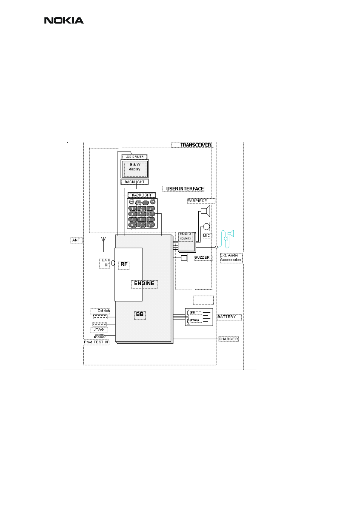
Transceiver RH-41 (Nokia 2260)
Introduction
The RH-41 is a dual band transceiver unit designed for TDMA800/1900 networks. The
transceiver consists of the engine module (ST6_11) and the various assembly parts.
The transceiver has a full graphic display and the user interface is based on a Jack style
UI with two soft keys. An internal antenna is used in the phone, and there is no connection to an external antenna. The transceiver also has a low leakage tolerant earpiece and
an omnidirectional microphone that provides excellent audio quality.
Figure 1: Interconnecting Diagram
Issue 2 09/2003 Nokia Corporation Confidential Page 9
Page 10

RH-41
System Module CCS Technical Documentation
Operational Modes
Below is a list of the phone’s different operational modes:
1 Power Off mode
2 Normal Mode (Power controlled by cellular SW, includes various Active and Idle
states):
• Analog Modes (800 MHz only):
•Analog Control Channel, ACCH
•Analog Voice Channel, AVCH
• Digital Modes (800 and 1900 MHz):
•Control Channel, DCCH
•Digital Voice Channel, DTCH (Digital Traffic Channel)
•Digital Data Channel, DDCH
Both the analog and digital modes have different states controlled by the Cellular SW.
Some examples are Idle State (on ACCH), Camping (on DCCH), Scanning, Conversation,
NSPS (No Service Power Save, previously OOR = Out of Range).
3 Local mode (both Cellular SW and UI SW non active)
4 Test mode (Cellular SW active but UI SW non active)
Environmental Specifications
Normal and extreme voltages
Voltage range:
• nominal battery voltage: 3.6 V
• maximum battery voltage: 5.0 V
• minimum battery voltage: 3.1 V
Temperature Conditions
Temperature range:
• ambient temperature: -30...+ 60
o
C
• PWB temperature: -30...+85 oC
Page 10 Nokia Corporation Confidential Issue 2 09/2003
Page 11
RH-41
Y
K
A
CCS Technical Documentation System Module
• storage temperature range: -40 to + 85 oC
All of the EIA/TIA-136-270A requirements are not exactly specified over the temperature
range. For example, the RX sensitivity requirement is 3dB lower over the –30 - +60 °C
range.
Engine Module
Baseband Module
The core part of the transceiver’s baseband (see the figure below) consists of two ASICs
— the UEM and UPP — and flash memory. The following sections illustrate and explain
these parts in detail.
RFIC CTRL
RF IC
RFCLK
19.44MHz
UPP
MEMADDA
MEMCONT
FLASH 16Mbit
PA supply
RF Supplies
RF RX/TX
PURX
RF RX/TX
SLEEPCLOC
32kHz
CBUS/DBUS
UDIO
BB Supplies
UEM
BATTER
EAR
MIC
BUZZER
KLIGHT/
DLIGHT
PWR ON
BASEBAND
CHARGER CONNECTION
EXTERNAL AUDIO
LCD
DCT4 System Connector
Figure 2: System Block Diagram
Issue 2 09/2003 Nokia Corporation Confidential Page 11
Page 12
RH-41
System Module CCS Technical Documentation
UEM
Introduction to UEM
UEM is the Universal Energy Management IC for digital hand portable phones. In addition to energy management, it performs all the baseband’s mixed-signal functions.
Most UEM pins have 2kV ESD protection, and those signals considered to be more easily
exposed to ESD, have 8kV protection within the UEM. These kinds of signals are (1) all
audio signals, (2) headset signals, (3) BSI, (4) Btemp, (5) Fbus, and (6) Mbus signals.
Regulators
The UEM has six regulators for baseband power supplies and seven regulators for RF
power supplies. The VR1 regulator has two outputs: (1) VR1a and (2) VR1b. In addition to
these, there are two current generators — IPA1 and IPA2 — for biasing purposes.
A bypass capacitor (1uF) is required for each regulator output to ensure stability.
Reference voltages for regulators require external 1uF capacitors. Vref25RF is the reference voltage for the VR2 regulator, Vref25BB is the reference voltage for the VANA,
VFLASH1, VFLASH2, VR1 regulators, Vref278 is the reference voltage for the VR3, VR4,
VR5, VR6, VR7 regulators, and VrefRF01 is the reference voltage for the VIO, VCORE regulators and for the radio frequency (RF).
BB RF Current
VANA: 2.78Vtyp 80mA max VR1a:4.75V 10mA max
VR1b:4.75V
Vflash1: 2.78Vtyp 70mA max IPA2: 0-5mA
Vflash2: 2.78Vtyp
40mA max
VIO: 1.8Vtyp
150mA max
Vcore: 1.0-1.8V
200mA max
VR2:2.78V 100mA max
VR4: 2.78V 50mA max
VR5: 2.78V 50mA max
VR6: 2.78V 50mA max
VR7: 2.78V 45mA max
IPA1: 0-5mA
The VANA regulator supplies the baseband’s (BB) internal and external analog circuitry.
It is disabled in the Sleep mode.
The Vflash1 regulator supplies the LCD, the digital parts of the UEM and Taco ASIC. It is
enabled during startup and goes into the low Iq-mode when in the Sleep mode.
The VIO regulator supplies both the external and internal logic circuitries. It is used by
the LCD, flash and UPP. The regulator goes into the low Iq-mode when in the Sleep mode.
Page 12 Nokia Corporation Confidential Issue 2 09/2003
Page 13

RH-41
CCS Technical Documentation System Module
The VCORE regulator supplies the DSP and the core part of the UPP. The voltage is programmable and the startup default is 1.5V. The regulator goes into the low Iq-mode
when in the Sleep mode.
The VR1 regulator uses two LDOs (VR1A and VR1B) and a charge pump. The charge pump
requires one external 1uF capacitor in the Vpump pin and a 220nF flying capacitor
between the CCP and CCN pins. In practice, the 220nF flying capacitor is formed by 2 x
100nF capacitors that are parallel to each other. The VR1A regulator is used by the Taco
RF ASIC.
The VR2 regulator is used to supply the (1) external RF parts, (2) lower band up converter, (3) TX power detector module, and (4) Taco. In light load situations, the VR2 regulator can be set to the low Iq-mode.
The VR3 regulator supplies the VCTCXO and Taco in the RF. It is always enabled when the
UEM is active. When the UEM is in the Sleep mode, the VR3 is disabled.
The VR4 regulator supplies the RX frontends (LNA and RX mixers).
The VR5 regulator supplies the lower band PA. In light load situations, the VR5 regulator
can be set to the low Iq-mode.
The VR6 regulator supplies the higher band PA and TX amplifier. In light load situations,
the VR6 regulator can be set to the low Iq-mode.
The VR7 regulator supplies the VCO and Taco. In light load situations, the VR7 regulator
can be set to the low Iq-mode.
The IPA1 and IPA2 are programmable current generators. A 27Ω/1%/100ppm external
resistor is used to improve the accuracy of the output current. The IPA1 is used by the
lower PA band and IPA2 is used by the higher PA band.
RF Interface
The interface between the baseband and the RF section is also handled by the UEM. It
provides A/D and D/A conversion of the in-phase and quadrature receive and transmit
signal paths. It also provides A/D and D/A conversions of received and transmitted audio
signals to and from the UI section. The UEM supplies the analog AFC signal to the RF section, according to the UPP DSP digital control.
Charging Control
The CHACON block of the UEM asics controls charging. The needed functions for the
charging controls are the (1) pwm-controlled battery charging switch, (2) charger-monitoring circuitry, (3) battery voltage monitoring circuitry, and (4) RTC supply circuitry for
backup battery charging (Not used in RH-41). In addition to these, external components
are needed for EMC protection of the charger input to the baseband module.
Digital Interface
Data transmission between the UEM and the UPP is implemented using two serial con-
Issue 2 09/2003 Nokia Corporation Confidential Page 13
Page 14

RH-41
System Module CCS Technical Documentation
nections, DBUS (programmable clock) for DSP and CBUS (1.0MHz GSM and 1.08MHz
TDMA) for MCU. The UEM is a dual voltage circuit: the digital parts are run from 1.8V
and the analog parts are run from 2.78V. The Vbat (3,6V) voltage regulators's input is
also used.
Audio Codec
The baseband supports two external microphone input areas and one external earphone
output. The input can be taken from an internal microphone, a headset microphone or
from an external microphone signal source through a headset connector. The output for
the internal earpiece is a dual-ended type output, and the differential output is capable
of driving 4Vpp to the earpiece with a 60 dB minimum signal as the total distortion ratio.
The input and output signal source selection and gain control is performed inside the
UEM Asic, according to the control messages from the UPP.
UI Drivers
There is a single output driver for the buzzer, display, and keyboard LEDs inside the UEM.
These generate PWM square wave for the various devices.
AD Converters
The UEM is equipped with an 11-channel analog-to-digital converter. Some AD converter
channels (LS, KEYB1-2) are not used in RH-41. The AD converters are calibrated in the
production line.
UPP
Introduction
RH-41 uses the UPPv4M ASIC. The RAM size is 4M. The processor architecture consists of
both the DSP and the MCU processors.
Blocks
The UPP is internally partitioned into two main parts: (1) the Brain and (2) the Body.
1 The Processor and Memory System (that is, the Processor cores, Mega-cells,
internal memories, peripherals and external memory interface) is known as the
Brain.
The Brain consists of the following blocks: (1) the DSP Subsystem (DSPSS), (2) the
MCU Subsystem (MCUSS), (3) the emulation control EMUCtl, (4) the program/
data RAM PDRAM, and (5) the Brain Peripherals–subsystem (BrainPer).
2 The NMP custom cellular logic functions are known as the Body.
The Body contains interfaces and functions needed for interfacing other baseband and RF parts. The body consists of, for example, the following sub-blocks:
(1) MFI, (2) SCU, (3) CTSI, (4) RxModem, (5) AccIF, (6) UIF, (7) Coder, (8) BodyIF,
and (9) PUP.
Page 14 Nokia Corporation Confidential Issue 2 09/2003
Page 15

RH-41
CCS Technical Documentation System Module
Flash Memory
Introduction
The RH-41 transceiver uses a 16-Mbit flash as its external memory. The VIO regulator is
used as a power supply for normal in-system operation. An accelerated program/erase
operation can be obtained by supplying Vpp of 12 volt to the flash device.
The device has two read modes: asynchronous and burst. The burst read mode is utilized
in RH-41, except for the start-up, when the asynchronous read mode is used for a short
time.
User Interface Hardware
LCD
Introduction
RH-41 uses a black-and-white GD46 84x48 full dot matrix graphical display. The LCD
module includes the LCD glass, the LCD COG-driver, an elastomer connector, and a metal
frame. The LCD module is included in the lightguide assembly module.
Interface
The LCD is controlled by the UI SW and the control signals are from the UPP ASIC. The
VIO and Vflash1 regulators supply the LCD with power.
The LCD has an internal voltage booster and a booster capacitor is required between
Vout and GND.
Pin 3 (Vss9) is the LCD driver’s ground and Pin 9 (GND) is used to ground the metal
frame.
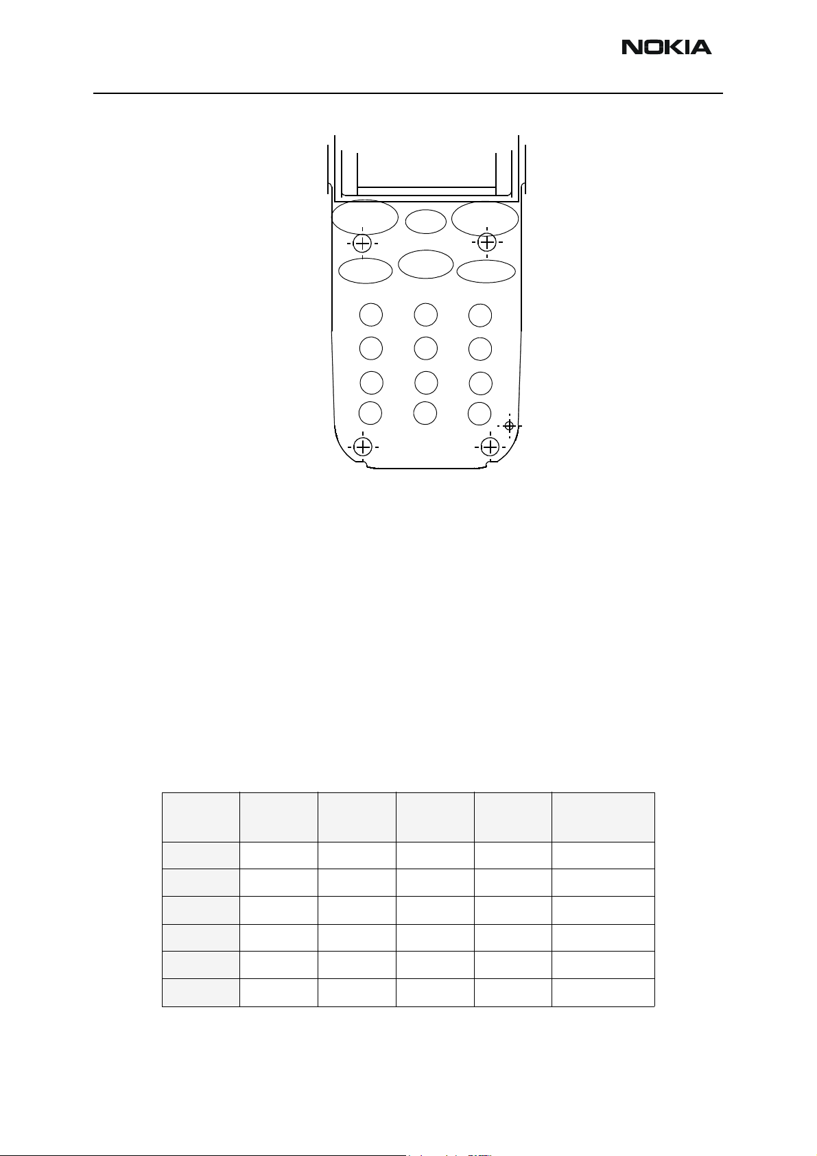
Keyboard
Introduction
The RH-41 keyboard style follows the Nokia Jack style, without side keys for volume control. The PWR key is located at the top of the phone.
Issue 2 09/2003 Nokia Corporation Confidential Page 15
Page 16
RH-41
System Module CCS Technical Documentation
Power Key
All signals for the keyboard come from the UPP ASIC, except PWRONX line for the power
key signal which is connected directly to the UEM. The pressing of the PWR key grounds
the PWRONX line and the UEM generates an interrupt to UOO, which is then recognized
as a PWR key press.
Up
Down
S RightS Left
EndSend
12 3
4
7
*
Figure 3: Placement of keys
56
8
0
#
9
Keys
Other keys are detected so that when a key is pressed down, the metal dome connects
one S-line and one R-line of the UPP together and creates an interrupt for the SW. This
kind of detection is also known as metaldome detection. The matrix of how lines are connected and which lines are used for different keys is described in the following table. The
S-line S0 and R-line R5 are not used at all.
Returns /
Scans
R0 NC NC Send End NC
R1 NC Soft left Up Down Soft right
R2 NC 1 4 7 *
R3 NC 2 5 8 0
R4 NC 3 6 9 #
R5 NC NC NC NC NC
S0 S1 S2 S3 S4
where NC = Not Connected
Page 16 Nokia Corporation Confidential Issue 2 09/2003
Page 17

RH-41
CCS Technical Documentation System Module
Lights
Introduction
RH-41 has blue LEDs for lighting purposes. The LED type is blue-light emitting and SMD
through-hole mounted.
Interfaces
The display lights are controlled by a Dlight signal from the UEM. The Dlight output is the
PWM signal, which is used to control the average current going through the LEDs. When
the battery voltage changes, the new PWM value is written onto the PWM register. In
this way, the brightness of the lights remains the same with all battery voltages within
range. The frequency of the signal is fixed at 128 Hz.
The keyboard lights are controlled by the Klight signal from the UEM. The Klight output is
also a PWM signal and is used in the same way as Dlight.
Technical Information
Each LED requires a hole in the PWB, in which the body of the LED locates in hole and
terminals are soldered on the component side of the module PWB. The LEDs have a white
plastic body around the diode, and this directs the emitted light better to the UI side. The
current for the LCD and keyboard lights is limited by the resistor between the Vbatt and
LEDs.
Audio HW
Earpiece
Introduction
The speaker is a dynamic one. It is very sensitive and capable of producing relatively high
sound pressure also at low frequencies. The speaker capsule and the mechanics around it
together make the earpiece.
Microphone
Introduction
The microphone is an electret microphone with an omnidirectional polar pattern. It consists of an electrically polarized membrane and a metal electrode which form a capacitor.
Air pressure changes (for example, sound) moves the membrane, which causes voltage
changes across the capacitor. Because the capacitance is typically 2 pF, a FET buffer is
needed inside the microphone capsule for the signal generated by the capacitor. Because
of the FET, the microphone needs a bias voltage.
Buzzer
Introduction
The operating principle of the buzzer is magnetic. The diaphragm of the buzzer is made
Issue 2 09/2003 Nokia Corporation Confidential Page 17
Page 18

RH-41
y
System Module CCS Technical Documentation
of magnetic material and it is located in a magnetic field created by a permanent magnet. The winding is not attached to the diaphragm, as is the case with the speaker. The
winding is located in the magnetic circuit so that it can alter the magnetic field of the
permanent magnet, thus changing the magnetic force affecting the diaphragm. The
buzzer's useful frequency range is approximately from 2 kHz to 5 kHz.
Battery
Phone Battery
Introduction
The BMC-3 battery (Ni-MH 900mAh) is the standard RH-41 battery. It is also possible to
use the BLC-2 (Li-ion 950mA) battery.
Interface
The battery block contains NTC and BSI resistors for temperature measurement and battery identification. The BSI fixed resistor value indicates the chemistry and default
capacity of a battery. The NTC-resistor measures the battery temperature. Temperature
and capacity information is needed for charge control. These resistors are connected to
BSI and BTEMP pins of the battery connector. The phone has pull-up resistors for these
lines so that they can be read by A/D inputs in the phone (see the figure below). Serial
resistors in the BSI and BTEMP lines are for ESD protection. Both lines also have spark
caps to prevent ESD. There is also a varistor in the BTEMP line for ESD protection.
UEM
C240
10n
R202/2
100k
R206
4k7
R207
4k7
VFLASH1
VANA
R202/1
100k
C101
10p
C220
10n
VBAT
Batter
connector
VBATT
BSI
BTEMP
GND
OVERCHARGE/
OVERDISCHARGE
PROTECTION
Figure 4: Battery Connection Diagram
The batteries have a specific red line, which indicates if the battery has been subjected to
excess humidity (red line spreads). The batteries are delivered in the protection mode,
which gives longer storage time. The voltage seen in the outer terminals is zero (or floating), and the battery is activated by connecting the charger. The battery has internal protection for overvoltage and overcurrent.
Ni-MH
Page 18 Nokia Corporation Confidential Issue 2 09/2003
Page 19

RH-41
(
V
)
CCS Technical Documentation System Module
Excess
humidity
indicator
Figure 5: BMC-3 Battery contacts (BLC-2 has the same interface)
Battery Connector
RH-41 uses the spring-type battery connector. This makes the phone easier to assemble
in production and the connection between the battery and the PWB is more reliable.
Battery Connector Interface
Signal
#
name
1 VBAT (+)
2 BSI BSI
3 BTEMP BTEMP
Connected from - to
VBAT I/O Vbat 3.0-5.1V Battery voltage
(batt.)
UEM Out Ana Battery size
(batt.)
UEM Out Ana 40mA/Switch
(batt.)
2(BSI)3(BTEMP)4(GND)
Batt. I/OSignal properties
A/D--levels--freq./timing
3
BAT
400mA
Description /
Notes
indicator
Battery temperature indicator
4 GND GND GND GND GND Ground
Accessories Interface
System connector
Introduction
RH-41 uses accessories via a system connector.
Interface
The interface is supported by fully differential 4-wire (XMICN, XMICP, XEARN, and
XEARP) accessories. RH-41 supports the HDE-2 inbox headset, HDB-5 Boom headset,
HDC-5 headset, LPS-3 loopset, and the PPH-1 car kit.
Issue 2 09/2003 Nokia Corporation Confidential Page 19
Page 20

RH-41
p
System Module CCS Technical Documentation
GND
VIN
PWMO
HEADINT HFC
XMICP
XMICN
HF
MICN MIC
Figure 6: System Connector
An accessory is detected by the HeadInt- line, which is connected to the XEARP inside
the system connector. When an accessory is connected, it disconnects XEARP from
HEADINT, and the UEM detects it and generates an interrupt (UEMINT) to the MCU. After
that, the HOOKINT line is used to determine which accessory is connected. This is done
by the voltage divider, which consists of the phone's internal pull-up and accessory-specific pull-down. The voltage generated by this divider is then read by the ad- converter of
UEM. The HOOKINT- interrupt is generated by the button in the headset or by the accessory external audio input.
2.7V
Hookint
/MBUS
EAD
HeadintHeadint
MIC1Bias
HF
HFCM
UEM
MIC1P
MIC1N
3...25k
2.1V
33n
33n
0.8V
100
Figure 7: Accessory Detection / External Audio
2k2
1.8V
0.3V
MicGND
Page 20 Nokia Corporation Confidential Issue 2 09/2003
Page 21

RH-41
CCS Technical Documentation System Module
Technical Information
ESD protection is made up by (1) spark caps, (2) a buried capacitor (Z152 and Z154-157),
and (3) ±8kV inside the UEM. The RF and BB noises are prevented by inductors.
PPH-1 Handsfree
Introduction
The PPH-1 handsfree device
• provides the charging and handsfree functionality,
• has a built-in speaker, and
• uses a phone microphone, but also has a connector for the HFM-8 optional external
microphone (using HFM-8 mutes phone microphone).
Interface
A 4-wire interface is implemented with 2.5 mm diameter round plug/jack which is otherwise like a so-called standard stereo plug, but the innermost contact is split into two.
2. XEARN
4. XEARP
5. HEADINT
3. XMICP
1. XMICN
Charger IF
Introduction
The charger connection is implemented through the system connector. The system connector supports charging with both plug chargers and desktop stand chargers.
There are three signals for charging. The charger GND pin is used for both desktop and
plug chargers as well as for charger voltage. The PWM control line, which is needed for
3-wire chargers, is connected directly to the GND in the PWB module, so the RH-41
engine does not provide any PWM control for chargers. Charging controlling is done
inside the UEM by switching the UEM’s internal charger switch on and off.
Interface
Figure 8: 4-wire, fully differential headset connector pin layout
The fuse (F100) protects the phone from too-high currents; for example, when broken or
pirate chargers are used. L100 protects the engine from RF noises, which may occur in
the charging cable. V100 protects the UEM ASIC from reverse-polarity charging voltage
and from too-high charging voltages. C106 is also used for ESD and EMC protection.
Spark gaps right after the charger plug are used for ESD protection.
Issue 2 09/2003 Nokia Corporation Confidential Page 21
Page 22

RH-41
P
X
System Module CCS Technical Documentation
Test Interfaces
Production Test Pattern
The interface for RH-41 production testing is a 5-pin pad layout in the BB area (see the
following figure). The production tester connects to these pads by using spring connectors. The interface includes the MBUS, FBUSRX, FBUSTX, VPP, and GND signals. The pad
size is 1.7 mm. The same pads are used also for AS test equipment, such as the module
jig and the service cable.
Other Test Points
As BB asics and flash memory are CSP components, the visibility of BB signals is very
poor. This makes the measuring of most of the BB signals impossible. In order to debug
the BB, at least to some level, the most important signals can be accessed from the
0.6 mm test points. The figure below shows the test points located between the UEM and
the UPP. There is an opening in the baseband shield to provide access to these pads.
2.
FBUS_T
6.
VP
3.
FBUS_RX
7.
MBUS
Figure 9: Top View of Production Test Pattern
8.
GND
UEM (D200)
CBUSDA
J407
J405
U P P (D 400 )
CBUSENX
J408
J415
DBUSEN1X
CBUSCLK
J406
J412
FBUSRX
FBUSTX
J411
J409
MBUSTX MBUSRX
J410
J414
DBUSCLKDBUSDA
J403
J413
J402
PURXSLEEPX
SLEEPCLK
J404
UEMINT
Figure 10: Test points located between UEM and UPP
Page 22 Nokia Corporation Confidential Issue 2 09/2003
Page 23

RH-41
CCS Technical Documentation System Module
EMC
General
The EMC/ESD performance of RH-41’s baseband is improved by using a shield to cover
the main components of the BB, such as the UEM, UPP, and Flash. The UEM has internal
protection against a ±8kV ESD pulse in most sensitive pins and ±2kV in other pins. The
BB shield is soldered to the PWB and it also increases the rigidity of the PWB in the BB
area, thus improving the phone’s reliability. The shield also improves the thermal dissipation by spreading the heat more widely.
The BB and RF shield are connected together on the PWB and the protective metal deck
underneath the battery is grounded to RF shield.
BB Component and Control IO Line Protection
Keyboard lines
ESD protection for keyboard signals is implemented by using separate EMI filter component located between keyboard and UPP. EMI component is a low-pass filter with ±15kV
ESD protection. Also the distance from A-cover to PWB is made longer with the spikes in
the keymat together with C-cover metallization is protecting keyboard lines.
C-Cover
The C-cover on the UI side is metallized on the inner surface (partly) and is grounded. All
areas in which the plated C-cover touches the PWB surface are grounded and the solder
masks are opened.
PWB
All edges are grounded on both sides of the PWB and the solder mask is opened in these
areas. The aim is that any ESD pulse faces the ground area first when entering the phone,
for example, between the mechanics covers.
LCD
ESD protection for LCD is implemented by connecting the metal frame of the LCD into
ground. The connection is only on one side, at the top of the LCD, which is not the best
solution. The software takes care of the LCD's crashing in case of an ESD pulse.
Microphone
The microphone’s metal cover is connected to the GND and there are spark gaps on the
PWB. The microphone is an asymmetrical circuit, which makes it well protected against
EMC.
EARP
The EARP is protected with C-cover metallization and with a plastic-fronted earpiece.
Buzzer
PWB openings with the C-cover metallization protect the buzzer from ESD.
Issue 2 09/2003 Nokia Corporation Confidential Page 23
Page 24

RH-41
System Module CCS Technical Documentation
System Connector Lines
System Connector signals that have EMC protection
Protection type VIN XMIXP XMICN XEARP XEARN HEADINT MICP
ferrite bead (600
/199MHz)
ferrite bead (420
/100MHz)
spark gaps XXXXXX
PWB capacitors XXXXXX
RC-circuit XXXXX
capacitor to
ground
X
XXXXX
XXXX X
Battery Connector Lines
BSI and BTEMP lines are protected by spark gaps and the RC circuit (4k7 and 10n), in
which the resistors are size 0603.
MBUS and FBUS
The opening in the protective metal deck, underneath the battery, is so small that ESD
does not get into the MBUS and FBUS lines in the production test pattern.
Transceiver Interfaces
The tables in the following sections illustrate the signals between the various transceiver
blocks.
BB - RF Interface Connections
The BB and RF parts are connected together without a physical connector.
All the signal descriptions and properties in the following tables are valid only for active
signals, and the signals are not necessarily present all the time.
Note: In the following tables, the nominal signal level of 2.78V is sometimes referred to as 2.7V.
Page 24 Nokia Corporation Confidential Issue 2 09/2003
Page 25

RH-41
CCS Technical Documentation System Module
Issue 2 09/2003 Nokia Corporation Confidential Page 25
Page 26

RH-41
System Module CCS Technical Documentation
Page 26 Nokia Corporation Confidential Issue 2 09/2003
Page 27

RH-41
CCS Technical Documentation System Module
Issue 2 09/2003 Nokia Corporation Confidential Page 27
Page 28

RH-41
System Module CCS Technical Documentation
BB Internal Connections
Page 28 Nokia Corporation Confidential Issue 2 09/2003
Page 29

RH-41
CCS Technical Documentation System Module
Issue 2 09/2003 Nokia Corporation Confidential Page 29
Page 30

RH-41
System Module CCS Technical Documentation
Page 30 Nokia Corporation Confidential Issue 2 09/2003
Page 31

RH-41
CCS Technical Documentation System Module
Issue 2 09/2003 Nokia Corporation Confidential Page 31
Page 32

RH-41
System Module CCS Technical Documentation
Page 32 Nokia Corporation Confidential Issue 2 09/2003
Page 33

RH-41
CCS Technical Documentation System Module
UPP Block Signals
Issue 2 09/2003 Nokia Corporation Confidential Page 33
Page 34

RH-41
System Module CCS Technical Documentation
Page 34 Nokia Corporation Confidential Issue 2 09/2003
Page 35

RH-41
CCS Technical Documentation System Module
Issue 2 09/2003 Nokia Corporation Confidential Page 35
Page 36

RH-41
System Module CCS Technical Documentation
Page 36 Nokia Corporation Confidential Issue 2 09/2003
Page 37

RH-41
CCS Technical Documentation System Module
Memory Block Interfaces
Issue 2 09/2003 Nokia Corporation Confidential Page 37
Page 38

RH-41
System Module CCS Technical Documentation
Audio Interfaces
Page 38 Nokia Corporation Confidential Issue 2 09/2003
Page 39

RH-41
CCS Technical Documentation System Module
Issue 2 09/2003 Nokia Corporation Confidential Page 39
Page 40

RH-41
System Module CCS Technical Documentation
Key/Display blocks
Keyboard Interface
Display Interface
RF Module
Requirements
The RH-41 RF module supports the following systems:
• AMPS
• TDMA 800
• TDMA 1900
The minimum transceiver performance requirements are described in TIA/EIA-136-270.
The RH-41 RF must follow the requirements in the revision A. The EMC requirements are
set by FCC 47CFR 15.107 (conducted emissions), 15.109 (radiated emissions, idle mode),
and 22.917 (radiated emissions, call mode).
The dualband RF module is capable of seamless operation between the 800 MHz and
Page 40 Nokia Corporation Confidential Issue 2 09/2003
Page 41

RH-41
CCS Technical Documentation System Module
1900 MHz bands, with measuring capability for cross-band hand-off and maho-measurements.
Design
The RF design is centered around the Taco RF-IC. Taco consists of receivers, transmitter IF
parts, highband TX upconverter, lowband TX upconverter, and all PLLs, lowband LNA, TX
VHF VCO active part, and loopfilter.
RF filtering, 2G LNA, power amplifiers, and TX power detection circuitry are left outside
Taco.
The phone is comprised of one single-sided, six–layer PWB. A single multiwall RF shield is
used and this sets the maximum component height to 2.0 mm. An internal antenna is
located on the top of the phone and there is room for a 4.0 mm high ceramic duplexer
under the antenna assembly.
Software Compensations
The following software compensations are required:
• Power levels temperature compensation
• Power levels channel compensation
• Power level reduction due to low battery Voltage
• TX Power Up/Down Ramps
• PA's bias reference currents vs. power, temp and operation mode
• RX IQ DC offsets
• RSSI channel compensation
Main Technical Characteristics
RF Frequency Plan
The RH-41 frequency plan is shown in the following figure. A 19.44 MHz VCTCXO is used
for UHF and VHF PLLs and as a baseband clock signal. All RF locals are generated in PLLs.
Issue 2 09/2003 Nokia Corporation Confidential Page 41
Page 42

RH-41
d
System Module CCS Technical Documentation
Rx Channel Centre Frequencies
TDMA1900 1930.05...1989
Rx Channel Centre Frequencies
TDMA800 869.04...893 .97 MHz
Tx channel centre frequencies
TDMA800 824.01...848 .97 MHz
Tx channel centre frequencies
TDMA1900 1850.01...1909
.99 MHz
.95 MHz
Rx IF
135.54 MHz
Rx IF
0 MHz
RX IQ
Rx VHF
271.08 MHz
VCTCXO
19.44 MHz
BaseBan
F
2
UHF
TDMA800 2009.16 MHz 2059.02 MHz
TDMA1900 RX: 2065. 59 MHz 2125.53 MHz
TDMA1900 TX: 20 31.81 MHz 2091.75 MHz
F
2
PLL
PLL
PLL
F
TDMA800 and1900: 361.08 MHz
Tx VHF
2
TX IQ
The RX intermediate frequency is the same on both operating bands. Due to the AMPS
mode, simultaneous reception and transmission, TX and RX IF frequencies are exactly
45 MHz apart. RXIF is 135.54 MHz and TXIF is 180.54 MHz. The RXIF frequency is set so
that it is not a multiple of either of VHF's comparison frequency (120k). In digital modes
(TDMA800/1900), RXIF frequency is also 135.54 MHz and TXIF is same (180.54MHz) with
all modes (TDMA800/1900).
DC Characteristics
Power Distribution Diagram
Note: The current values in the following figure are not absolute values and cannot be measured.
These values represent maximum/typical currents drawn by the corresponding RF or Taco blocks in
use, and are, therefore, dependent on the phone’s operating mode and state.
Tx IF
180.54 MHz
Figure 11: RF Frequency Block Plan
Page 42 Nokia Corporation Confidential Issue 2 09/2003
Page 43

RH-41
U
L
CCS Technical Documentation System Module
UEM
VR1a
2 mA
VR2
VR3
VR4
VR5
IPA1
1 mA
Pwr Det
1 mA
VCTCXO
5 mA
5 mA
PA 800
630 mA
40 mA
38/36 mA
60 mA
0.9 mA
0.5 mA
6.0 mA
12 mA
4.3/5.6 mA
Taco
TACO
UHF phasedet.
TX VHF VCO
2G TX mixer
TX-IF
1G TX mixer
REF_in / REF_out
biasing
RX 1st mixer
RX-IF
LNA / LNA_bias
VCC_CP
VCC_TXMIX
VCC_TX
VCC_TXMIX
VCC_REF
VCC_RX
VCC_RX
VCC_RX
VCC_LNA
VFLASH1
VREFRF01
Regulators
The regulator circuit is the UEM and the specifications can be found in the following
table:
IPA2
VR7
5 mA
VBATT 3.1-5.0 V
10 mA
PA 1900
2G VCO
2G LNA
750 mA
4.1/4.7 mA
Figure 12: Power distribution
6.7/5.1 mA
0/10 mA
10 /0mA
4.5 mA
5.6 mA
0.8 mA
50 uA
TXVHF PLL
RXVHF PLL
RX 1st mixer
HF PL
LO buff (2G TX mix)
LO buff (1G TX mix)
REF_in + PLLs
bias reference
VCC_TX2
VCC_RX2
VCC_PLL
VCC_PLL
VCC_PLL
VCC_PLL
VCC_DIGI
VREF
Issue 2 09/2003 Nokia Corporation Confidential Page 43
Page 44

RH-41
System Module CCS Technical Documentation
Regulator name Output voltage (V)
VR1 a/b 4.75 ± 3% 10 4 4
VR2 2.78 ± 3% 100 100 76
VR3 2.78 ± 3% 20 2 2
VR4 2.78 ± 3% 50 23 24
VR5 2.78 ± 3% 50 5 5
VR6 2.78 ± 3% 50 5 5
VR7 2.78 ± 3% 45 40 45
IPA1, IPA2 2.7 max. 1 ± 10%
VREFRF01 1.35 ± 0.5% 0.12 0.05 0.05
VFLASH1 2.78 ± 3% 70 1 1
Regulator Max.
current (mA)
3 ± 4%
3.5 ± 4%
5 ± 3%
RF total 1 GHz RF total 2 GHz
1.3 – 5.0 1.3 – 3.7
Receiver
The receiver shows a superheterodyne structure with zero 2nd IF. Lowband and highband
receivers have separate frontends from the diplexer to the first IF. Most of the receiver
functions are integrated in the RF ASIC. The only functions out of the chip are highband
LNA, duplexers and SAW filters. In spite of a slightly different component selection, the
receiver characteristics are very similar on both bands.
An active 1st downconverter sets naturally high gain requirements for preceding stages.
Hence, losses in very selective frontend filters are minimized down to the limits set by
filter technologies used and component sizes. LNA gain is set up to 16dB, which is close
to the maximum available stable gain from a single stage amplifier. LNAs are not exactly
noise matched in order to keep passband gain ripple in minimum. Filters have relative
tight stopband requirements, which are not all set by the system requirements but the
interference free operation in the field. In this receiver structure, linearity lies heavily on
mixer design. The 2nd order distortion requirements of the mixer are set by the 'half IF'
suppression. A fully balanced mixer topology is required. Additionally, the receiver 3rd
order IIP tends to depend on active mixer IIP3 linearity due to pretty high LNA gain.
IF stages include a narrowband SAW filter on the 1st IF and a integrated lowpass filtering on zero IF. SAW filter guarantees 14dBc attenuation at alternating channels, which
gives acceptable receiver IMD performance with only moderate VHF local phase noise
performance. The local signal's partition to receiver selectivity and IMD depends then
mainly on the spectral purity of the 1st local. Zero 2nd IF stages include most of receivers signal gain, AGC control range and channel filtering.
Page 44 Nokia Corporation Confidential Issue 2 09/2003
Page 45

RH-41
CCS Technical Documentation System Module
ITEM NMP Requirement
TDMA, AMPS
800
RX frequency range, DAMPS 800 869.01...
893.97
LO frequency range 2009.1...
2059.2
1st IF frequency 135.54
Channel NBW, RF 28.6
IF 1 3dB roll off min. frequency (+-?f) 13
2nd IF min. 3dB bandwidth 16 / IQ-branch
Max total group delay at 3dB bandwidth
C/N for sensitivity, digital
analog
C/I for selectivity, digital
analog
Sensitivity, digital mode static ch (BER < 3%)
ANALOG MODE (sinad >12dB)
7
3.5
8
4
-110 (min.)
-116 (min.)
TDMA 1900
1930.050...
1989.990
2065.59...
2125.53
-110 (min.)
Adjacent channel selectivity, digital
analog
Alternate channel selectivity, digital
analog
IMD attentuation selectivity, digital
analog close spaced (60/120)
analog wide spaced (330/660)
Cascaded NF, digital
analog
Cascaded IIP 3, digital 120/240, 240/480 kHz
analog 60/120 kHz
analog 330/660 kHz
Available receiver gain digital/analog 85 (min.)
RF front end gain control range, AGC 1 step 20
1st IF gain control range, AGC 2 step 30
R X 2nd IF gain control range, 8x6dB steps 42
Min signal level at RX-ADC input @ sensitivity
digital
analog
13
16*
45
65*
65
65*
70*
< 9.5
< 9.5
> -7.7
> -17*
> -8*
-31
-25
13
45
65
< 9.5
> -8
-31
Input dynamic range -116... -20
Issue 2 09/2003 Nokia Corporation Confidential Page 45
Page 46

RH-41
System Module CCS Technical Documentation
ITEM NMP Requirement
Gain relative accuracy in receiving band ** 2
Gain absolute accuracy in receiving band ** 4
* referenced to the sensitivity level
** After production alignment
AMPS/TDMA 800 MHz Front End
Typical values.
Parameter MIN TYP MAX Unit/Notes
Diplexer input loss 0.35 0.4 0.45 dB
Duplexer input loss 2.5 3 4.1 dB
LNA gain: High gain mode
Low gain mode
LNA noise figure* 1.4 1.7 2.3 dB
LNA 3rd order intercept (IIP3)* -4 -3 -1.5 dBm
Bandfilter input loss 1.5 2 2.5 dB
Mixer gain* 6 7.5 8 dB
Mixer NF* 8 9 10.5 dB
Mixer IIP3* 4 4.5 5 dBm
Total:
Gain 18.2 18.6 20 dB
Noise Figure 4.6 5.5 7 dB
3rd order intercept (IIP3) -8.9 -7.5 -6.8 dBm
*see Taco spec/measurements
16
-4.5
16.5
-4
17.3
-3.8
TDMA 1900 MHz Front End
TDMA 1900 LNA is discrete. It uses integrated Bias control block, which is inside Taco. In
the normal high-gain operation mode, the bias voltage 2.78V is connected onto the collector and the sink type constant current source is connected onto the emitter. The bias
current source is adjustable from 0.5 mA to 7.5 mA with 0.5 mA step. The base is biased
from 2.78V voltage via resistor.
dB
dB
When LNA AGC step is enabled, LNA is in low gain operation mode. Voltage and current
bias sources and direction of current are switched on the contrary. In this operation
mode the LNA has good linearity, still low noise figure and about -3 dB gain.
During TX slot LNA is in power-down mode, which is executed by switching the bias current source to 0 mA.
Page 46 Nokia Corporation Confidential Issue 2 09/2003
Page 47

RH-41
CCS Technical Documentation System Module
Parameter MIN TYP MAX Unit/Notes
Diplexer input loss 0.45 0.5 0.55 dB
Duplexer input loss 1.3 2.5 3.0 dB
LNA gain: High gain mode
Low gain mode
LNA noise figure* 1.0 1.2 1.5 dB
LNA 3rd order intercept (IIP3)* -3 -2 -1 dBm
Bandfilter input loss 3.6 4.5 dB
Mixer gain* 6.5 7.5 8.5 dB
Mixer NF* 9 10 11 dB
Mixer IIP3* 4 4.5 5 dBm
Total:
Gain 16.0 17.0 18.0 dB
Noise Figure 5.0 5.5 6.5 dB
3rd order intercept (IIP3) 4 5 6 dB
*see Taco spec/measurements -70 -68 dBc
14
-3.5
15
-3.0
15.5
-2.0
dB
dB
Parameter Minimum
Total
Power up time 0.1 ms
Noise figure, total 9.5 dB
3rd order input intercept point -25 dBm
Max voltage gain,
Mixer + 2nd IF (IF+2nd AGC max)
Min voltage gain,
Mixer + 2nd IF (IF+2nd AGC min.)
Gain charge,
Mixer+2nd IF
IQ mixers + AMP2
RF input impedance differential 1.2 kohm/pF
RF input frequency range 135.54 MHz
78.5 dB
Typical/
Nominal
1.4 0.9 dB, temp
Maximum Unit/Notes
6dB
-30...+85 C
Issue 2 09/2003 Nokia Corporation Confidential Page 47
Page 48

RH-41
System Module CCS Technical Documentation
Parameter Minimum
Conversion gain @ RI=1kohm 23.5 24 24.5 dB
IF AGC gain range (5x6 dB) 30 dB
IF AGC gain step (5 steps) 6 dB
IF AGC gain error relative to max
gain
AMP2 gain 18 dB
-3dB frequency 21 25 29 kHz
LPF: 4th order Chebysev
LPF gain 0 dB
Corner frequency tuning range 14 17 kHz
Corner frequency tuning step 1 kHz
Attentuation @ 30 kHz * 24 dB
Attentuation @ 60 kHz * 55 dB
Attentuation @ 120 kHz * 80 dB
-0.5 +0.5 dB
Typical/
Nominal
Maximum Unit/Notes
Attentuation @ 240 kHz * 60 dB
Attentuation @ >480 kHz * 40 dB
AGC
AGC gain range -6 36** dB
AGC gain range step
7 steps
AGC gain error relative to max gain -0.5 +0.5 dB
Max IF/2nd IF buffer output level 3 V pp (differential)
6dB
Frequency Synthesizers
RH-41 synthesizer consists of three synthesizers: one UHF synthesizer and two VHF synthesizers. UHF synthesizer is based on integrated PLL and external UHF VCO, loop filter,
and VCTCXO. Its main goal is to achieve the channel selection, thus for dual band operations associated with dual mode. Due to the RX and TX architecture this UHF synthesizer
is used for down-conversion of the received signal and for final up-conversion in transmitter. A common 2 GHz UHFVCO module is used for operation on both low- and highband. Frequency divider by two is integrated in Taco.
Two VHF synthesizers consist of: RX VHF Synthesizer, includes integrated PLL and VCO,
and external loop filter and resonator. The output of RX-VHF PLL is used as LO signal for
the second mixer in receiver. TX VHF Synthesizer includes integrated PLL, loop filter, and
resonator. The output of TX-VHF PLL is used as a LO signal for the IQ-modulator of the
transmitter. See depicted block diagrams and synthesizer characteristics from synthesizer
Page 48 Nokia Corporation Confidential Issue 2 09/2003
Page 49

RH-41
CCS Technical Documentation System Module
specification document [6].
Transmitter
The transmitter RF architecture is up-conversion type (desired RF spectrum is low side
injection) with (RF) modulation and gain control at IF. The IF frequency is band-related
being 180.54 MHz at cellular band and 181.80 MHz at PCS band. The cellular band is
824.01 MHz - 848.97 MHz and PCS band is 1850.01MHz -1909.95MHz.
Common IF
The RF modulator is integrated with Programmable Gain Amplifier (PGA) and IF output
buffer inside Taco_T RFIC-chip. I- and Q-signals, that are output signals from BB-side
SW IQ-modulator, have some filtering inside Taco before RF modulation is performed.
The required LO-signal from TXVCO is buffered with phase sifting in Taco. After modulation (π/4 DQPSK or FM), the modulated IF signal is amplified in PGA.
Cellular Band
At operation in cellular band the IF signal is buffered at IF output stage that is enabled
by TXP1 TX control. The maximum linear (balanced) IF signal level to 50Ω load is about
-8 dBm.
For proper AMPS mode receiver (duplex) sensitivity, IF signal is filtered in strip filter
before up-conversion. The up-converter mixer is actually a mixer with LO and output
driver being able to deliver about +6dBm linear output power. Note, that in this point,
term linear means –33dB ACP. The required LO power is about –6dBm. The LO signal is
fed from Taco.
Before power amplifier RF signal is filter in band filter. The typical insertion loss is about
–2.7dB, and maximum less than –3.5dB. Input and output return losses are about –10dB.
Power amplifier is 50Ω/50Ω module. It does not have own enable/disable control signal,
but it can be enabled by bias voltage and reference bias current signals. The gain window
is +27 to +31dB and linear output power is +30dBm (typical condition) with –28dB ACP.
The nominal efficiency is 50%.
PCS Band
At operation in PCS band, the IF signal is routed outside from Taco to be filtered in TX IF
SAW filter, and after that back to Taco, to the up-converter mixer. The LO signal to the
mixer is buffered and balanced inside Taco. The mixer output is enabled by TXP2 TX control signal. The maximum linear (balanced) RF signal level to 50Ω load is about +7dBm.
After Taco-balanced RF signal is single-ended in 1:1 balun and then filtered in SAW filter. The typical insertion loss is about –4.0dB, and maximum less than –5.7dB. This filter
has relatively high pass band ripple (about 1.0-1.5dB), largest insertion being at high end
of the band. The input and return losses are about –10dB.
Power amplifier is 50Ω/50Ω module. It does not have own enable/disable control signal,
but it can be enabled by bias voltage and reference bias current signals. The gain window
Issue 2 09/2003 Nokia Corporation Confidential Page 49
Page 50

RH-41
System Module CCS Technical Documentation
is +31 to +36dB and linear output power is +30dBm (typical condition) with –28dB ACP.
The nominal efficiency is 40%.
Power Control
For power monitoring, there is a power detector module (PDM) build up from a (dual)
coupler, a biased diode detector, and an NTC resistor. RF signals from both bands are
routed via this PDM. The RF isolation between couplers is sufficient not to lose filtering
performance given by duplex filters.
The diode output voltage and NTC voltage are routed to BB A/D converters for power
control purposes. The TX AGC SW takes samples from diode output voltage and compares
that value to target value, and adjust BB I-and Q-signal amplitude and/or Taco PGA settings to keep power control in balance.
NTC voltage is used for diode temperature compensation and for thermal shutdown
when radio board’s temperature exceeds +85°C.
False TX indication is based on detected power measurement when carrier is not on.
The insertion loss of coupler is –0.42dB (max) at cellular band and –0.48dB (max) at PCS
band. Typical values for insertion losses are about –0.2dB. The filtering performance of
diplexer is taken in account in system calculations.
Antenna Circuit
Here the antenna circuit stands for duplex filters and the diplexer. The cellular band
duplex filter is band pass type SAW filter with typical insertion loss about –2.0dB. The
PCS band duplex filter is band stop (for receiver band) type ceramic filter and its typical
insertion loss is about –1.7dB. Insertion losses of diplexer are –0.45dB and –0.55dB (at
maximum) for cellular and PCS band, typical values being about –0.30dB and -0.35dB.
RF Performance
The output power tuning target for power level 2 after diplexer (or after switch for external RF) is +27.3dBm for digital modes and +24.8 dBm for analog mode. See the following
table. Modulation accuracy and ACP will be within limits specified in IS-136/137.
Page 50 Nokia Corporation Confidential Issue 2 09/2003
Page 51

RH-41
CCS Technical Documentation System Module
Power Level
Antenna
The RH-41 antenna solution is an internal, dual-resonance PIFA. This antenna has a common feeding point for both antenna radiators, which results in the need for a diplexer. In
a single band transceiver, an SMD-compatible through-chip can be used.
2
3
4
5
6
7
8
9
10
PGA
3
4
5
6
7
8
9
10
11
Pout
TDMA800 TDM1900 AMPS
27.3 27.3 24.8
23.3 23.3 21.6
19.3 19.3 18.5
15.3 15.3 14.5
11.3 11.3 10.5
7.3 7.3 6.5
3.3 3.3 -
-0.7 -0.7 -
-4.7 -4.7 -
Issue 2 09/2003 Nokia Corporation Confidential Page 51
Page 52

RH-41
System Module CCS Technical Documentation
Page 52 Nokia Corporation Confidential Issue 2 09/2003
 Loading...