

Page 1

PAMS Technical Documentation
NSW-6 Series Transceivers
System Module SE2
Issue 1 12/99 Nokia Mobile Phones Ltd.
Page 2
NSW-6
System Module SE2
PAMS Technical Documentation
AMENDMENT RECORD SHEET
Amendment
Number
Date Inserted By Comments
12/99 OJuntune
Page 2
Nokia Mobile Phones Ltd.
Issue 1 12/99
Page 3

PAMS Technical Documentation
CONTENTS
Transceiver NSW–6 7. . . . . . . . . . . . . . . . . . . . . . . . . . . . . . . . . . . . .
Introduction 7. . . . . . . . . . . . . . . . . . . . . . . . . . . . . . . . . . . . . . . . . .
External Connectors and Main Interfaces 7. . . . . . . . . . . . . . . . . .
External and Internal Connectors 7. . . . . . . . . . . . . . . . . . . . . . .
Contacts Description 8. . . . . . . . . . . . . . . . . . . . . . . . . . . . . . . . . .
Battery Connector 9. . . . . . . . . . . . . . . . . . . . . . . . . . . . . . . . . . . .
Charging Connector 9. . . . . . . . . . . . . . . . . . . . . . . . . . . . . . . . . .
Headset Connector 10. . . . . . . . . . . . . . . . . . . . . . . . . . . . . . . . . .
Baseband Module, Functional Description 11. . . . . . . . . . . . . . . . . .
Modes of Operation 11. . . . . . . . . . . . . . . . . . . . . . . . . . . . . . . . . . .
Analog Control Channel mode (ACCH) 11. . . . . . . . . . . . . . . .
Analog Voice Channel Mode (AVCH) 11. . . . . . . . . . . . . . . . .
Digital Control Channel Mode (DCCH) 12. . . . . . . . . . . . . . . .
Digital Traffic Channel Mode (DTCH) 12. . . . . . . . . . . . . . . . .
Out of Range mode (OOR) 13. . . . . . . . . . . . . . . . . . . . . . . . . .
Locals Mode 13. . . . . . . . . . . . . . . . . . . . . . . . . . . . . . . . . . . . . . .
Technical Summary 13. . . . . . . . . . . . . . . . . . . . . . . . . . . . . . . . . . .
List of Submodules 13. . . . . . . . . . . . . . . . . . . . . . . . . . . . . . . . .
Baseband Submodules 14. . . . . . . . . . . . . . . . . . . . . . . . . . . . . . . .
CTRLU 14. . . . . . . . . . . . . . . . . . . . . . . . . . . . . . . . . . . . . . . . . . .
MCU main features 15. . . . . . . . . . . . . . . . . . . . . . . . . . . . . . . . .
DSP Main Features 17. . . . . . . . . . . . . . . . . . . . . . . . . . . . . . . .
System Logic main Features 17. . . . . . . . . . . . . . . . . . . . . . . . .
Memories 17. . . . . . . . . . . . . . . . . . . . . . . . . . . . . . . . . . . . . . . . .
AUDIO–RF 17. . . . . . . . . . . . . . . . . . . . . . . . . . . . . . . . . . . . . . . . . .
COBBA Main Features 17. . . . . . . . . . . . . . . . . . . . . . . . . . . . . .
PWRU 18. . . . . . . . . . . . . . . . . . . . . . . . . . . . . . . . . . . . . . . . . . . . . .
CCONT Main Features 18. . . . . . . . . . . . . . . . . . . . . . . . . . . . .
CHAPS Main Features 18. . . . . . . . . . . . . . . . . . . . . . . . . . . . . .
NSW-6
System Module SE2
Page No
Clocking 19. . . . . . . . . . . . . . . . . . . . . . . . . . . . . . . . . . . . . . . . . . . . . . .
System Clock 19. . . . . . . . . . . . . . . . . . . . . . . . . . . . . . . . . . . . . . . .
Sleep Clock 19. . . . . . . . . . . . . . . . . . . . . . . . . . . . . . . . . . . . . . . . . .
Resets 20. . . . . . . . . . . . . . . . . . . . . . . . . . . . . . . . . . . . . . . . . . . . . . . .
Power–up reset 20. . . . . . . . . . . . . . . . . . . . . . . . . . . . . . . . . . . . . .
Other reset 20. . . . . . . . . . . . . . . . . . . . . . . . . . . . . . . . . . . . . . . . . .
Power Distribution 21. . . . . . . . . . . . . . . . . . . . . . . . . . . . . . . . . . . .
Power Up 22. . . . . . . . . . . . . . . . . . . . . . . . . . . . . . . . . . . . . . . . . . .
Power up with a charger 23. . . . . . . . . . . . . . . . . . . . . . . . . . . .
Normal Battery voltage 23. . . . . . . . . . . . . . . . . . . . . . . . . . .
Empty Battery 24. . . . . . . . . . . . . . . . . . . . . . . . . . . . . . . . . .
Issue 1 12/99
Nokia Mobile Phones Ltd.
Page 3
Page 4

NSW-6
System Module SE2
Power Up by IBI 24. . . . . . . . . . . . . . . . . . . . . . . . . . . . . . . . . . .
Mixed Trigger to power up 25. . . . . . . . . . . . . . . . . . . . . . . . . . .
Power Down 25. . . . . . . . . . . . . . . . . . . . . . . . . . . . . . . . . . . . . . . . .
Controlled Power Down 25. . . . . . . . . . . . . . . . . . . . . . . . . . . . .
Power Down pushing PWR key 25. . . . . . . . . . . . . . . . . . . .
Power Down when the battery voltage is discharged 25.
Power Down with fault in transmitter 25. . . . . . . . . . . . . . . .
Uncontrolled Power Down 25. . . . . . . . . . . . . . . . . . . . . . . . . . .
Power Down when Watchdog expires 25. . . . . . . . . . . . . .
Battery Disconnected 26. . . . . . . . . . . . . . . . . . . . . . . . . . . . .
Battery Disconnected when charger is connected 26. . . .
Sleep Mode 26. . . . . . . . . . . . . . . . . . . . . . . . . . . . . . . . . . . . . . . . . .
Entering the Sleep mode 26. . . . . . . . . . . . . . . . . . . . . . . . . . . .
Waking up from the Sleep mode 26. . . . . . . . . . . . . . . . . . . . .
Charging Control 27. . . . . . . . . . . . . . . . . . . . . . . . . . . . . . . . . . . . .
Two–wire Charging 27. . . . . . . . . . . . . . . . . . . . . . . . . . . . . . . . .
Three–wire Charging 27. . . . . . . . . . . . . . . . . . . . . . . . . . . . . . .
Watchdog 28. . . . . . . . . . . . . . . . . . . . . . . . . . . . . . . . . . . . . . . . .
Battery Overvoltage Protection 28. . . . . . . . . . . . . . . . . . . . . . .
Battery Identification 29. . . . . . . . . . . . . . . . . . . . . . . . . . . . . . . .
Battery Temperature 30. . . . . . . . . . . . . . . . . . . . . . . . . . . . . . . .
Supply Voltage Regulators 30. . . . . . . . . . . . . . . . . . . . . . . . . .
Audio Control 31. . . . . . . . . . . . . . . . . . . . . . . . . . . . . . . . . . . . . . . .
Internal Microphone and Earpiece 32. . . . . . . . . . . . . . . . . . . .
External Audio Connections 33. . . . . . . . . . . . . . . . . . . . . . . . .
Audio Accessory Detection 33. . . . . . . . . . . . . . . . . . . . . . . .
Internal Audio Connections (speech processing) 33. . . . . . .
4–wire PCM Serial Interface 34. . . . . . . . . . . . . . . . . . . . . . . . .
Speech Processing 34. . . . . . . . . . . . . . . . . . . . . . . . . . . . . . . . .
Alert Signal Generation 35. . . . . . . . . . . . . . . . . . . . . . . . . . . . .
Digital Control 36. . . . . . . . . . . . . . . . . . . . . . . . . . . . . . . . . . . . . . . .
MAD 36. . . . . . . . . . . . . . . . . . . . . . . . . . . . . . . . . . . . . . . . . . . . .
Memories 37. . . . . . . . . . . . . . . . . . . . . . . . . . . . . . . . . . . . . . . . .
Program Memory 16MBit Flash 37. . . . . . . . . . . . . . . . . . . .
SRAM Memory 37. . . . . . . . . . . . . . . . . . . . . . . . . . . . . . . . . .
EEPROM Emulated in FLASH Memory 37. . . . . . . . . . . . .
Flash Programming 37. . . . . . . . . . . . . . . . . . . . . . . . . . . . . . . .
PAMS Technical Documentation
RF Module 39. . . . . . . . . . . . . . . . . . . . . . . . . . . . . . . . . . . . . . . . . . . . .
Technical Summary 39. . . . . . . . . . . . . . . . . . . . . . . . . . . . . . . . . . .
RF Frequency Plan 39. . . . . . . . . . . . . . . . . . . . . . . . . . . . . . . . . . .
DC Characteristics 40. . . . . . . . . . . . . . . . . . . . . . . . . . . . . . . . . . . .
Power Distribution Diagram 40. . . . . . . . . . . . . . . . . . . . . . . . . .
Regulators 42. . . . . . . . . . . . . . . . . . . . . . . . . . . . . . . . . . . . . . . .
Receiver 42. . . . . . . . . . . . . . . . . . . . . . . . . . . . . . . . . . . . . . . . . . . .
DAMPS800 RX 42. . . . . . . . . . . . . . . . . . . . . . . . . . . . . . . . . . . .
Page 4
Nokia Mobile Phones Ltd.
Issue 1 12/99
Page 5

PAMS Technical Documentation
TDMA 1900 RX 43. . . . . . . . . . . . . . . . . . . . . . . . . . . . . . . . . . . .
Frequency Synthesizers 43. . . . . . . . . . . . . . . . . . . . . . . . . . . . . . .
DAMPS 800 operation 44. . . . . . . . . . . . . . . . . . . . . . . . . . . . . .
TDMA 1900 operation 44. . . . . . . . . . . . . . . . . . . . . . . . . . . . . .
Transmitter 44. . . . . . . . . . . . . . . . . . . . . . . . . . . . . . . . . . . . . . . . . .
DAMPS800 TX 44. . . . . . . . . . . . . . . . . . . . . . . . . . . . . . . . . . . .
TDMA1900 TX 45. . . . . . . . . . . . . . . . . . . . . . . . . . . . . . . . . . . . .
DAMPS800/TDMA1900 operation 45. . . . . . . . . . . . . . . . . . . . . .
Supply voltages in different modes of operation 45. . . . . . . .
Software Compensations 46. . . . . . . . . . . . . . . . . . . . . . . . . . . . . .
Power Levels (TXC) vs. Temperature 46. . . . . . . . . . . . . . . . .
Power Levels (TXC) vs. Channel 46. . . . . . . . . . . . . . . . . . . . .
Power levels vs. Battery Voltage 46. . . . . . . . . . . . . . . . . . . . .
TX Power Up/Down Ramps 46. . . . . . . . . . . . . . . . . . . . . . . . .
Digital Mode RSSI 46. . . . . . . . . . . . . . . . . . . . . . . . . . . . . . . . . .
RF Block Specifications 47. . . . . . . . . . . . . . . . . . . . . . . . . . . . . . . . . .
NSW-6
System Module SE2
Receiver 47. . . . . . . . . . . . . . . . . . . . . . . . . . . . . . . . . . . . . . . . . . . .
DAMPS 800MHz RX Front End 47. . . . . . . . . . . . . . . . . . . . . .
TDMA 1900MHz RX Front End 47. . . . . . . . . . . . . . . . . . . . . .
SAW Filter 48. . . . . . . . . . . . . . . . . . . . . . . . . . . . . . . . . . . . . . . .
Analog IF parts 48. . . . . . . . . . . . . . . . . . . . . . . . . . . . . . . . . . . .
Digital IF parts 49. . . . . . . . . . . . . . . . . . . . . . . . . . . . . . . . . . . . .
Transmitter 50. . . . . . . . . . . . . . . . . . . . . . . . . . . . . . . . . . . . . . . . . .
TX Power levels 50. . . . . . . . . . . . . . . . . . . . . . . . . . . . . . . . . . .
Synthesizers 51. . . . . . . . . . . . . . . . . . . . . . . . . . . . . . . . . . . . . .
UHF Synthesizers specification 51. . . . . . . . . . . . . . . . . . . .
VHF Synthesizers specification 51. . . . . . . . . . . . . . . . . . . .
Output levels 52. . . . . . . . . . . . . . . . . . . . . . . . . . . . . . . . . . . .
RF/BB interface signals 52. . . . . . . . . . . . . . . . . . . . . . . . . . . . . . .
Parts Lists 57. . . . . . . . . . . . . . . . . . . . . . . . . . . . . . . . . . . . . . . . . . . . .
Engine Module SE2 (0201320) 57. . . . . . . . . . . . . . . . . . . . . . . . .
Issue 1 12/99
Nokia Mobile Phones Ltd.
Page 5
Page 6

NSW-6
System Module SE2
PAMS Technical Documentation
CONTENTS
Schematics/ Layouts
Block Diagram of SE2 Module (Version 5100 Edit 118) 3A–1. . . . . . .
Circuit Diagram of BB (Version 5100 Edit 355) 3A–2. . . . . . . . . . . . . .
Circuit Diagram of CTRLU Block (Version 5100 Edit 400 ) 3A–3. . .
Circuit Diagram of PWRU (Version 5100 Edit 402 ) 3A–4. . . . . . . .
Circuit Diagram of Audio (Version 5100 Edit 315) 3A–5. . . . . . . . . .
Circuit Diagram of Receiver (Version 5100 Edit 229) 3A–6. . . . . . . .
Circuit Diagram of Synthesizer Block (Version 5100 Edit 188) 3A–7
Circuit Diagram of Transmitter (Version 5100 Edit 566) 3A–8. . . . . .
Circuit Diagram of RF–BB (Version 5100 Edit 101) 3A–9. . . . . . . . . .
Circuit Diagram of UI (Version 5100 Edit 173) 3A–10. . . . . . . . . . . . . .
Layout Diagram of JM1 1/2 3A–11. . . . . . . . . . . . . . . . . . . . . . . . . . . . .
Layout Diagram of JM1 2/2 3A–11. . . . . . . . . . . . . . . . . . . . . . . . . . . . . .
Page 6
Nokia Mobile Phones Ltd.
Issue 1 12/99
Page 7
PAMS Technical Documentation
Transceiver NSW–6
Introduction
The NSW–6 is a dual band triple mode radio transceiver designed for the
DAMPS and TDMA1900 networks, with 9 power levels and a maximum
output of 480mW.
The transceiver comprises of a System/RF module SE2 with integrated
user interface and assembly parts.
The transceiver features a full graphic display and a two soft–key based
user interface. The antenna is internal. External antenna connection is
not included. The transceiver also features a leakage tolerant earpiece
and a noise cancelling microphone.
NSW-6
System Module SE2
External Connectors and Main Interfaces
External and Internal Connectors
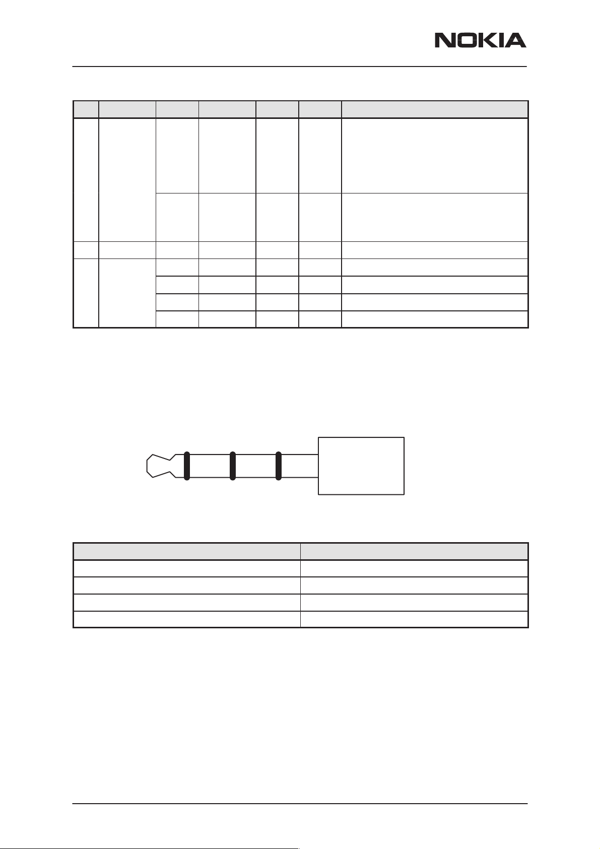
Supply Voltages and Power Consumption
Connector Line Symbol Minimum Typical /
Nominal
Charging VIN 7.1 8.4 9.3 V/ Travel charger,
Charging VIN 7.25 7.6 7.95 V/ Travel charger.
Charging I / VIN 720 800 850 mA/ Travel charger,
Charging I / VIN 320 370 420 mA/ Travel charger,
Maximum/
Peak
Unit / Notes
ACT–1
ACP–7, ACP–8
ACT–1
ACP–7
Issue 1 12/99
Nokia Mobile Phones Ltd.
Page 7
Page 8
NSW-6
System Module SE2
Battery contact signals
PAMS Technical Documentation
Pin Line
Symbol
1 BVOLT Battery voltage 3.0 3.6 5.3 V/ Maximum voltage in idle
2 BSI
3 BTEMP Input voltage
4 BGND 0 0 V
Parameter Mini-
mum
Input voltage 0 2.85 V/ Battery size indication
Battery indication
resistor
Input voltage
20 22 24 kohm/ service battery
27 51 kohm/ 4.1V Li battery
68 91 kohm/ 4.2V Li battery
0
2.1
Typical
/ Nomi-
nal
181% kohm/ Ni battery
Maxi-
mum
1.4
3
Unit / Notes
mode with a charger connected
Phone has 100k pull up resistor
V/ Battery temp. indication
V/ Phone power up (pulse)
Contacts Description
The transceiver electronics consist of the Radio Module ie. RF + System
blocks, the keyboard PCB, the display module and audio components.
The keypad and the display module are connected to the Radio Module
with connectors. System blocks and RF blocks are interconnected with
PCB wiring. The Transceiver is connected to accessories via charger con-
nector (includes jack and plates), and headset connector.
Page 8
The System blocks provide the MCU, DSP and Logic control functions in
MAD ASIC, external memories, audio processing and RF control hard-
ware in COBBA ASIC. Power supply circuitry CCONT ASIC delivers oper-
ating voltages both for the System and the RF blocks.
The RF block is designed for a handportable phone which operates in the
TDMA system. The purpose of the RF block is to receive and demodulate
the radio frequency signal from the base station and to transmit a modu-
lated RF signal to the base station
Nokia Mobile Phones Ltd.
Issue 1 12/99
Page 9
PAMS Technical Documentation
5.0
Maximum voltage in call state with charger
Battery Connector
Battery contact signals
Pin Name Min Typ Max Unit Notes
NSW-6
System Module SE2
4 BVOLT 3.0 3.6 4.5
5.3
3 BSI
2 BTEMP
0 2.85 V Battery size indication
181% kohm Battery indication resistor (Ni battery)
20 22 24 kohm Battery indication resistor (service battery)
33+/1 kohm Battery indication resistor (4.1V 600 mAh Lith-
47+/–
10%
0 1.4 V Battery temperature indication
2.1
1 10
1.9
90 100
3
20
2.85
200
V Battery voltage
Maximum voltage in idle state with charger
Phone has 100kohm pull up resistor.
SIM Card removal detection
(Threshold is 2.4V@VBB=2.8V)
ium battery)
kohm Battery indication resistor (Flash adapter)
Phone has a 100k (+–5%) pullup resistor,
Battery package has a NTC pulldown resistor:
47k+–5%@+25C , B=4050+–3%
V
ms
V
ms
Phone power up by battery (input)
Power up pulse width
Battery power up by phone (output)
Power up pulse width
1 BGND 0 0 V Battery ground
Charging Connector
Contact Line Symbol Function
DC–jack side contact
(DC–plug ring)
DC–jack center pin VIN Charger input voltage
DC–jack side contact
(DC–plug jacket)
Issue 1 12/99
L_GND Charger ground
CHRG_CTRL Charger control output (from phone)
Nokia Mobile Phones Ltd.
Page 9
Page 10
NSW-6
C
System Module SE2
Pin Name Min Typ Max Unit Notes
PAMS Technical Documentation
2, b VIN
3, a L_GND 0 0 V Supply ground
4, c CHRG_
TRL
7.25
3.25
320
7.1
3.25
720
0 0.5 V Charger control PWM low
2.0 2.85 V Charger control PWM high
1 99 % PWM duty cycle
7.6
3.6
370
8.4
3.6
800
32 Hz PWM frequency for a fast charger
7.95
16.9
3.95
420
9.3
3.95
850
V
V
V
mA
V
V
mA
Unloaded ACP–7 Charger (5kohms
load)
Peak output voltage (5kohms load)
Loaded output voltage (10ohms load)
Supply current
Unloaded ACP–9 Charger
Loaded output voltage (10ohms load)
Supply current
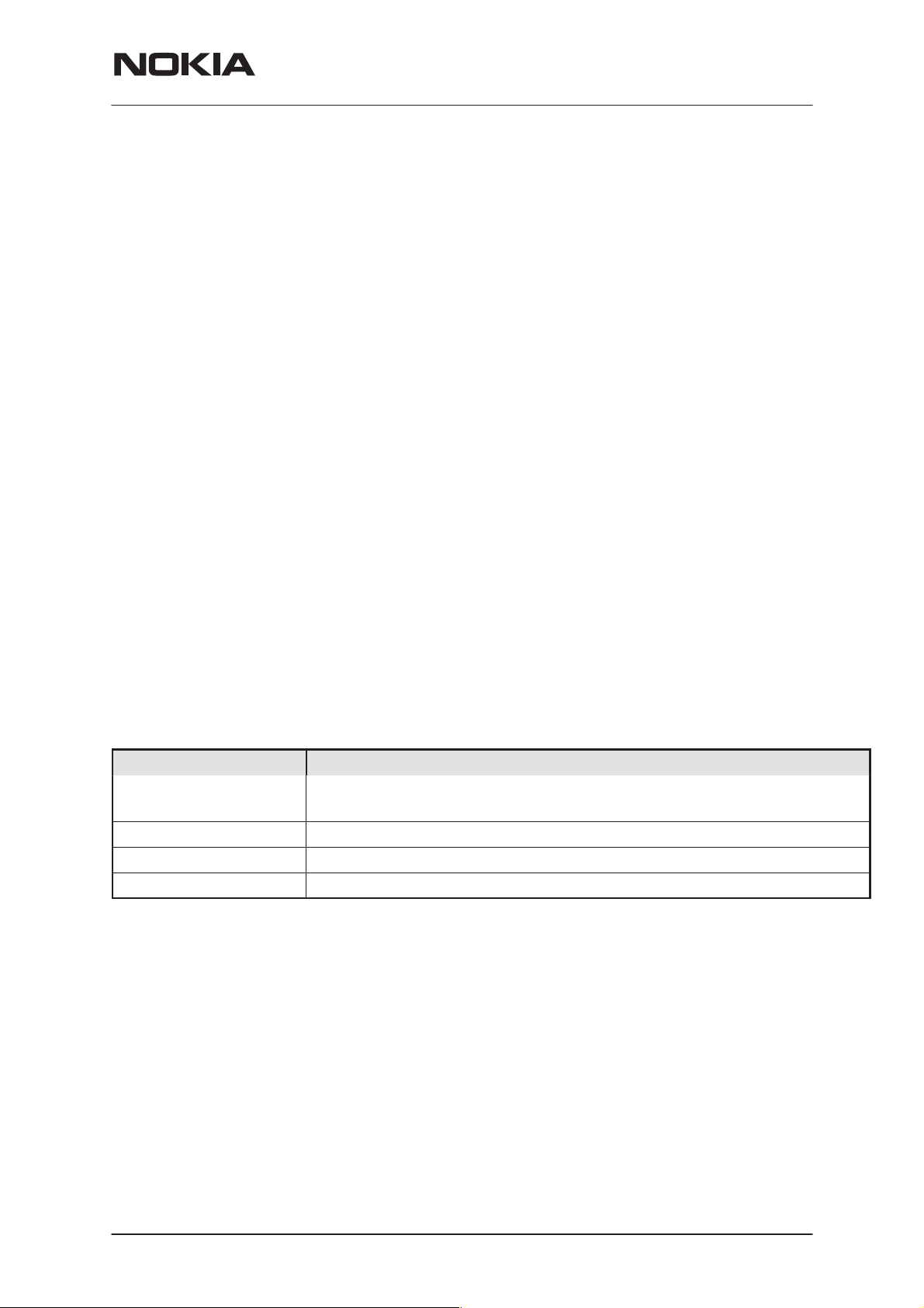
Headset Connector
The contacts of the headset connector are listed below, with the help of
the diagram of the headset plug.
HEADSET
PLUG
1234/5
Contact Line Symbol
1. contact (plug ring 1) XMICN
2. contact (plug ring 2) XEARN
3. contact (plug ring 3) XMICP
4. and 5. contact (center pin) XEARP (4) / HEADSETINT (5)
Page 10
Nokia Mobile Phones Ltd.
Issue 1 12/99
Page 11

PAMS Technical Documentation
System Module SE2
Baseband Module, Functional Description
Modes of Operation
The phone has the following main operating modes
– Analog mode, on 800 MHz band
– Analog Control Channel ACCH
– Analog Voice Channel AVCH
– Digital mode, on 800 MHz band
– Digital Control Channel DCCH
– Digital Traffic Channel DTCH
NSW-6
– Digital mode, on 1900 MHz band
– Digital Control Channel DCCH
– Digital Traffic Channel DTCH
– Out Of Range –mode OOR
– Locals mode
Analog Control Channel mode (ACCH
On analog control channel the phone receives continuous signalling
messages on Forward Control Channel (FOCC) from base station, being
most of the time in IDLE mode. Only the receiver part is on. Occasionally
the phone re–scans control channels in order to find the stronger or
otherwise preferred control channel.
Also registration (TX on) happens occasionally, whereby the phone sends
its information on Reverse Control Channel (RECC) to base station and
the phone’s location is updated in the switching office.
If a call is initiated, either by the user or base station, the phone moves to
analog voice channel or digital traffic channel mode depending on the
orders by the base station.
)
Analog Voice Channel Mode (AVCH)
The phone receives and transmits analog audio signal. All circuitry is
powered up except digital rx–parts. In this mode the DSP does all the audio processing and in the Hands Free (HF) mode it also performs echo–
cancellation and the HF algorithm. COBBA performs the AD–conversion
for the MIC signal, and the DA–conversion for the EAR signal.
Issue 1 12/99
Nokia Mobile Phones Ltd.
Page 11
Page 12

NSW-6
System Module SE2
With audio signal also SAT (Supervisory Audio Tone) is being received
from the base station. The SAT signal can be 5970 Hz, 6000Hz or 6030
Hz, the frequency being defined by the base station. DSP’s DPLL phase
lock loops to SAT, detects if the SAT frequency is the expected one and
examines the signal quality. DSP reports SAT quality figures to MCU regularly. The received SAT signal is transponded (transmitted back) to base
station.
The base station can send signalling messages on Forward Voice Channel (FVC) to the phone, by replacing the audio with a burst of Wide Band
Data (WBD). Typically these are handoff or power level messages. System Logic RX–modem is used for receiving the signalling message burst,
after which it gives interrupt to MCU for reading the data. During the burst
audio path must be muted; MCU gives message to DSP about this. MCU
can acknowledge the messages on Reverse Voice Channel (RVC), where
DSP sends the WBD to transmitter RF.
Also Signalling Tone (ST) can be transmitted to acknowledge messages
from base station. DSP sends ST after MCU’s command.
PAMS Technical Documentation
On Analog Voice Channel MCU uses sleep mode (HW DEEP SLEEP)
most of the time, but other circuits are fully operational.
Digital Control Channel Mode (DCCH)
On digital control channel (DCCH) DSP receives the paging information
from the Paging channels. DSP sends messages to MCU for processing
them.
Each Hyperframe (HFC) comprises two Superframes (SF), the first as
the Primary (p) and the second as the Secondary (s) paging frame. The
assigned Page Frame Class (PFC) defines the frames which must be received, and thus it also defines when the receiver must be on; i.e. the
basic power consumption is defined at the same time.
The phone employs sleep mode between received time slots. Then DSP
sets the sleep clock timer and MCU, DSP and RF including VCXO are
powered down. Only sleep clock and necessary timers are running.
From DCCH phone may be ordered to analog control channel or to analog or digital traffic channel.
Digital Traffic Channel Mode (DTCH)
Page 12
Digital Voice Channel
On digital voice channel DSP processes speech signal in 20 ms time
slots. DSP performs the speech and channel functions in time shared
fashion and sleeps whenever possible. Rx and tx are powered on and off
according to the slot timing. MCU is waken up mainly by DSP, when
there is signalling information for the Cellular Software.
Nokia Mobile Phones Ltd.
Issue 1 12/99
Page 13
PAMS Technical Documentation
Digital Data Channel
Digital Data Channel is supported in the product.
Out of Range mode (OOR)
If the phone cannot find signal from the base station on any control channel (analog or digital) it can go into OOR mode for power saving.
All RF circuits are powered off and baseband circuits are put into low
power mode, VCXO is stopped and only sleep clock is running in MAD
and CCONT. After the programmable timer in MAD has elapsed the
phone turns receiver on and tries to receive signalling data from base station. If it succeeds, the phone goes to standby mode on analog or digital
control channel. If the connection can not be established the phone will
return to out of range mode, until the timer elapses again.
Locals Mode
NSW-6
System Module SE2
Locals mode is used by product development, production and after sales,
for testing purposes. MCU’s Cellular Software is stopped (no signalling to
base station), and the phone is controlled by MBUS messages from test
PC.
Technical Summary
List of Submodules
Submodule Function
CTRLU Control Unit for the phone, comprising MAD ASIC (MCU, DSP,
System Logic) and Memories
PWRU Power supply, comprising CCONT and CHAPS
AUDIO_RF_IF Audio coding and RF–BB interface, COBBA
UI User Interface components
These blocks are only functional blocks and therefore have no type nor
material codes. For block diagram, see baseband schematics.
The battery voltage range in DCT3 family is 3.0V to 4.5V depending on
the battery charge and used cell type (Li–Ion or NiMH). Because of the
battery voltage the baseband supply voltage is a nominal of 2.8V.
The baseband is running from a 2.8V power rail which is supplied by a
power controlling asic (CCONT). In the CCONT there are seven
individually controlled regulator outputs for the RF section, one 2.8V
output for the baseband plus a core voltage for MAD1. In addition there is
one +5V power supply output(V5V). A real time clock function is integrated
into the CCONT which utilizes the same 32KHz clock supply as the sleep
clock. A backup power supply is provided for the RTC which keeps the
Issue 1 12/99
Nokia Mobile Phones Ltd.
Page 13
Page 14
NSW-6
System Module SE2
real time clock running when the main battery is removed. The backup
power supply is a rechargeable polyacene battery with a backup time of
ten minutes.
The interface between the baseband and the RF section is handled by a
specific asic. The COBBA_D asic provides A/D and D/A conversion of the
in–phase and quadrature receive and transmit signal paths and also A/D
and D/A conversions of received and transmitted audio signals to and
from the UI parts. Data transmission between the COBBA_D and the MAD
is implemented using serial connections. Digital speech processing is
handled by the MAD asic. The COBBA_D asic is a dual supply voltage
circuit, the digital parts are running from the baseband supply VBB and
the analog parts are running from the analog supply VCOBBA (VR6).
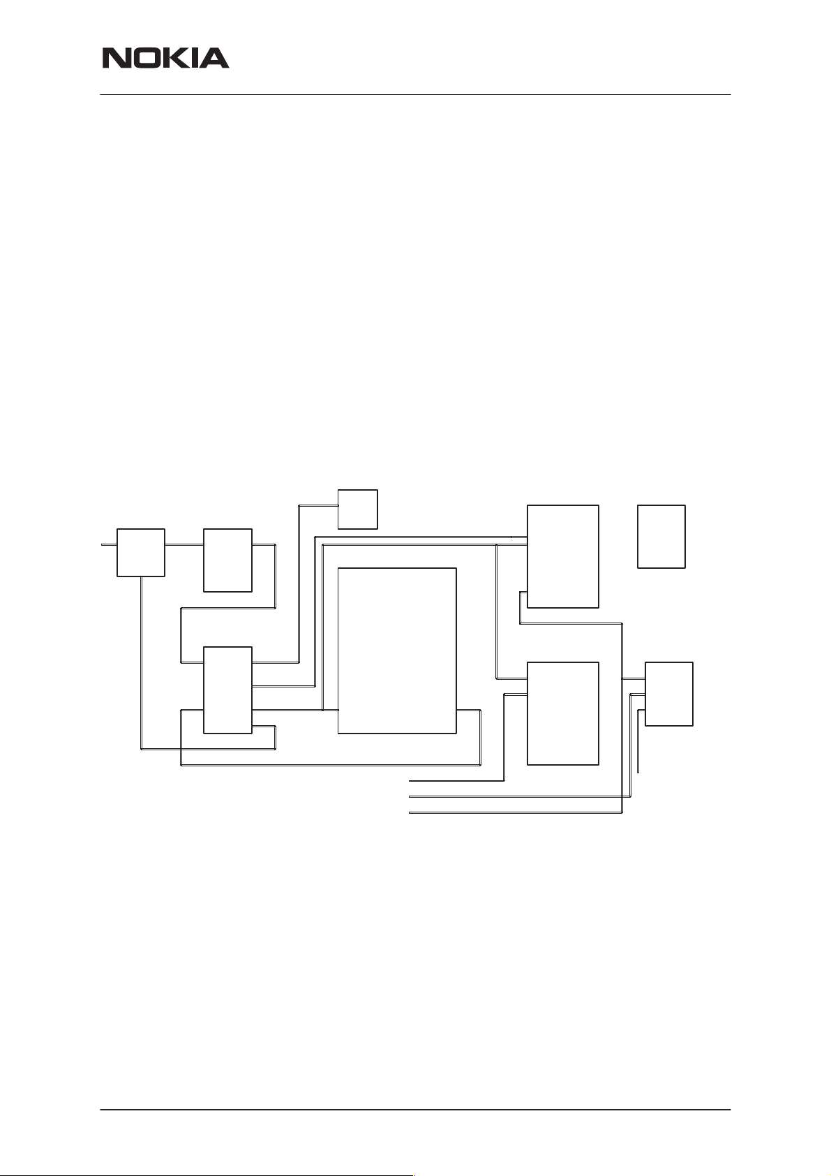
Block diagram for the phone is below.
PAMS Technical Documentation
LCD
vibra
motor
BASEBAND
TX/RX SIGNALS
COBBA SUPPLY
COBBA_P
AUDIOLINES
MAD1
+
MEMORIES
CHARGER conn
RF SUPPLIES
CCONT
BB SUPPLY
core voltage
CHAPS
PA SUPPL Y
32kHz
CLK
SLEEP CLOCK
VBAT
19.44M
CLK
SYSTEM CLOCK
BATTERY
NiMH LiIon
Baseband Submodules
CTRLU
CTRLU comprises MAD ASIC (MCU, DSP, System Logic) and Memories.
The environment consists of two memory circuits; (FLASH, SRAM),
22–bit address bus, and 16–bit data bus. Also there are ROM1SELX,
ROM2SELX, and RAMSELX signals for chip selection.
Page 14
Nokia Mobile Phones Ltd.
Issue 1 12/99
Page 15

PAMS Technical Documentation
MCU main features
System control
Cellular Software (CS)
Cellular Software communicates with the switching office, and
performs call build–up, maintenance and termination.
Communication control
M2BUS is used to communicate to external devices. This interface is also used for factory testing, service and maintenance purposes.
User Interface (UI)
PWR–key, keyboard, LCD, backlight, mic, ear and alert (buzzer, vibra, led) control. Serial interface from MAD to LCD
(same as for CCONT).
NSW-6
System Module SE2
Authentication
Authentication is used to prevent fraud usage of cellular
phones.
RF monitoring
RF temperature monitoring by VCXOTEMP, ADC in CCONT.
Received signal strength monitoring by RSSI, ADC in CCONT.
False transmission detection by TXF signal, digital IO–pin.
Power up/down and Watchdog control
When power key is pressed, initial reset (PURX) has happened
and default regulators have powered up in CCONT, MCU and
DSP take care of the rest of power up procedures (LCD, COBBA, RF). The MCU must regularly reset the Watchdog counter
in CCONT, otherwise the power will be switched off.
Accessory monitoring
Accessory detection by EAD (HEADSETINT), AD–converter in
CCONT.
Battery and charging monitoring
MCU reads the battery type (BTYPE), temperature (BTEMP)
and voltage (VBAT) values by AD–converter in CCONT, and
phone’s operation is allowed only if the values are reasonable.
Charging current is controlled by writing suitable values to
PWM control in CCONT.
Production/after sales tests and tuning
Control of CCONT via serial bus
Issue 1 12/99
MCU reads also charger voltage (VCHAR) and charging current values (ICHAR).
Flash loading, baseband tests, RF tuning
Nokia Mobile Phones Ltd.
Page 15
Page 16

NSW-6
System Module SE2
PAMS Technical Documentation
MCU writes controls (regulators on/off, Watchdog reset,
charge PWM control) and reads AD–conversion values. For
AD–conversions MCU gives the clock for CCONT (bus clock),
because the only clock in CCONT is sleep clock, which has a
too low frequency.
Page 16
Nokia Mobile Phones Ltd.
Issue 1 12/99
Page 17

PAMS Technical Documentation
DSP Main Features
DSP (Digital Signal Processor) is in charge of the channel and speech
coding according to the IS–136 specification. The block consists of a DSP
and internal ROM and RAM memory. The input clock is 9.72 MHz, and
DSP has its own internal PLL–multiplier. Main interfaces are to MCU, and
via System Logic to COBBA and RF.
System Logic main Features
– MCU related clocking, timing and interrupts (CTIM)
– DSP related clocking, timing and interrupts (CTID)
– DSP general IO–port
–reset and interrupts to MCU and DSP
– interface between MCU and DSP (API)
NSW-6
System Module SE2
– MCU interface to System Logic (MCUif)
– MCU controlled PWMs, general IO–port and USART for MBUS (PUP)
– Receive Modem (Rxmodem)
– Interface to Keyboard, CCONT and LCD Drivers (UIF)
– Interface to MCU memories, address lines and chip select decoding
(BUSC)
– DSP interface to System Logic (DSPif)
– serial accessory interface (AccIf, DSP–UART)
– Modulation, transmit filter and serial interface to COBBA (MFI)
– Serial interface for RF synthesizer control (SCU)
Memories
The speed of FLASH and SRAM is 120 ns.
FLASH
– size 1024k * 16 bit, contains the main program code for the MCU, and
is able to emulate EEPROM.
SRAM
– size 128k * 16 bit
AUDIO–RF
Audio interface and baseband–RF interface converters are integrated into
COBBA circuit.
COBBA Main Features
The codec includes microphone and earpiece amplifier and all the necessary switches for routing. There are two different possibilities for routing;
Issue 1 12/99
Nokia Mobile Phones Ltd.
Page 17
Page 18

NSW-6
System Module SE2
internal and external devices. There are also all the AD– and DA– converters for the RF interface.
DEMO block is used for FM–demodulation in analog mode.
A slow speed DA–converter provides automatic frequency control (AFC).
In addition, there is a DA–converters for transmitter power control (TXC).
COBBA also passes the RFC (19.44 MHz) to MAD as COBBACLK (9.72
MHz).
COBBA is connected to MAD via two serial buses:
– RXTXSIO, for interfacing the RF–DACs and DEMO; and also for audio
codec and general control. Signals used: COBBACLK (9.72 MHz, from
COBBA), COBBACSX, COBBASD (bi–directional data) and COBBADAX (data ready flag for rx–samples).
– Codec SIO, for interfacing the audio ADCs / DACs (PCM–samples).
Signals: PCMDCLK (data clock 1.08 MHz / 1.215 MHz), PCMSCLK
(frame sync 8.0 kHz / 8.1 kHz), PCMTxdata and PCMRxdata.
PAMS Technical Documentation
PWRU
PWRU comprises CCONT circuit and CHAPS circuit.
CCONT Main Features
CCONT generates regulated supply voltages for baseband and RF.
There are seven 2.8 V linear regulators for RF, one 2.8 V regulator for
baseband, one special switched output (VR1_SW), one programmable 2
V output (V2V), one 3/5 V output, one 5 V output, and one 1.5 V +/– 1.5
% reference voltage for RF and COBBA.
Other functions include:
– power up/down procedures and reset logic
– charging control (PWM), charger detection
– watchdog
– sleep clock (32.768 kHz) and control
– 8–channel AD–converter.
CHAPS Main Features
Page 18
CHAPS comprises the hardware for charging the battery and protecting
the phone from over–voltage in charger connector.
The main functions include
– transient, over–voltage and reverse charger voltage protection
– limited start–up charge current for a totally empty battery
– voltage limit when battery removed
– with SW protection against too high charging current
Nokia Mobile Phones Ltd.
Issue 1 12/99
Page 19
PAMS Technical Documentation
Clocking
System Clock
VR1
CHAPS
BATTERY
19.44MHz
VCXO
200mVpp–1Vpp
sine wave
MAD COBBA
NSW-6
System Module SE2
LCD–DRVR
LCDRESXRFC
PWRONX
32 kHz
. Clocking and resets
VCXO on RF provides the system clock for baseband (RFC). COBBA
squares the clock and divides it by two for MAD (COBBACLK).
This clock can be stopped by cutting supply voltage from VCXO (CCONT
regulator VR1) and started again by powering on the same regulator.
MAD controls it through RFCEN. It can be stopped only when both MCU
and DSP request that. It is always stopped in SLEEP–mode on control
channels. When the VCXO is stopped time is measures in MAD by using
the sleep clock SLCLK; when the programmable timer expires it gives interrupt to DSP/MCU and MAD also starts the VCXO power supply by
RFCEN signal.
CCONT
SLCLK
PURX
RFCEN
RFCSETTLED
COBBARESX
COBBACLK
9.72MHz
Square wave
2.8Vpp
The same sleep clock is also used in the MBUS interface, to detect if
there is communication on the bus during sleep periods.
Inside MAD System Logic parts provide clock signal to both DSP and
MCU, and both internal clocks can be stopped individually for power saving. MCU can use either CLOCK STOP or HW STANDBY sleep mode.
Sleep Clock
CCONT makes 32.768 kHz sleep clock for MAD. This crystal oscillator in
CCONT_2’ starts to run only after the battery is connected and the phone
Issue 1 12/99
Nokia Mobile Phones Ltd.
Page 19
Page 20

NSW-6
System Module SE2
has been started once. The SLCLK output is enabled only when the
baseband parts are powered up.
After the sleep periods, when the VCXO is restarted (by RFCEN), MAD
takes care that the clock is not used before it is properly settled. MAD output RFCSETTLED prevents COBBA from using the clock during the settling time (RFCSETTLED rises later than RFCEN), as well MAD internally
inhibits DSP and MCU during the same time. This settling time can be
programmed before going to sleep mode, and the sleep clock is used for
measuring the time.
Resets
Power–up reset
PAMS Technical Documentation
CCONT gives the power–up reset (PURX) to MAD and COBBA. Also display is reset via MAD output pin. During this reset the VCXO clock has
enough time to settle so that it can be used as the system clock after
reset.
Other reset
COBBA can be also internally reset; there are two internal reset bits in
COBBA registers which can be written by MAD.
LCD reset is possible also by by MCU SW, because the control pin pin is
controlled by MCU.
There are also MAD internal reset possibilities
– MCU can reset system logic parts
– MCU can reset DSP
– SW–watchdog can reset the whole MAD
Page 20
Nokia Mobile Phones Ltd.
Issue 1 12/99
Page 21
PAMS Technical Documentation
Power Distribution
In normal operation the baseband is powered from the phone‘s battery.
The battery consists of one Lithium–Ion cell. There is also a possibility to
use batteries consisting of three Nickel Metal Hydride cells or one Solid
state cell. An external charger can be used for recharging the battery and
supplying power to the phone. The charger can be either performance
charger, which can deliver supply current up to 850 mA or a standard
charger that can deliver approx. 300 mA.
The figure below is a simplified block diagram of the power distribution.
The power management circuitry provides protection against overvol-
tages, charger failures and pirate chargers etc. that could cause damage
to the phone.
NSW-6
System Module SE2
VCHAR
CHAPS
VBAT
PWM
BATTERY
CCONT
VR1
VR6
VBB
VCXO
MAD
VBB
V5V
Vref
SIO
COBBA LCD–DRVR
FLASH
RF
VR1–VR7
Battery voltage VBAT is connected to CCONT which regulates all the supply voltages VBB, VR1–VR7, VSIM and V5V. CCONT enables automatically VR1, VBB, VR6 and Vref in power–up.
VBB is used as baseband power supply for all digital parts. It is constantly
on when the phone is powered up.
VSIM is used as programming voltage for the Flash memory whenever a
partial re–flashing is needed, e.g. when the Flash emulates EEPROM.
V5V is used for RF parts only. In CCONT_2’ it also can be switched off by
using RFCEN signal.
Issue 1 12/99
Nokia Mobile Phones Ltd.
Page 21
Page 22

NSW-6
System Module SE2
VR1 is used for the VCXO supply, and VR6 is used in COBBA for analog
parts. RFCEN signal to CCONT controls both VR1 and VR6 regulators;
they can be switched off in sleep modes, and during standby. However,
VR6 output is not switched off, but connected to VBB inside CCONT, in
order to avoid false accessory interrupts.
CCONT regulators are controlled either through SIO from MAD or timing
sensitive regulators are controlled directly to their control pins. These two
control methods form a logical OR–function, i.e. the regulator is enabled
when either of the controls is active. Most of the regulators can be individually controlled.
CHAPS connects the charger voltage (VCHAR) to battery. MCU of MAD
controls the charging through CCONT. MAD sets the parameters to
PWM–generator in CCONT and PWM–output controls the charging voltage in charger.
When battery voltage is under 3.0 V, CHAPS controls independently the
charging current.
PAMS Technical Documentation
Power Up
When the battery is connected to phone, the 32.768 kHz crystal oscillator
of CCONT is not started, since CCONT2 version F, until the power–button
is pressed. (Oscillator start may take up to 1 second). The regulators are
not started. After the crystal has started, the phone is ready to be powered up by any of the ways described below.
Page 22
Nokia Mobile Phones Ltd.
Issue 1 12/99
Page 23

PAMS Technical Documentation
Power up with a charger
Normal Battery voltage
VCHAR
VR1, VBB, VR6
RFCEN
RFCSETTLED
RFC (VCXO)
COBBACLK
NSW-6
System Module SE2
PURX
SLCLK
CCONTINT
t1
t2
t3
The power up procedure is similar to process described in the previous
chapter with the exception that the rising edge of VCHAR triggers the
power up in CCONT.
Also CCONT sets output CCONTINT. MAD detects the interrupt, and after
that reads CCONT status register to find out the reason for the interrupt
(charger in this case). The phone will remain in the ”acting dead” state,
which means that the user interface is not activated unless the power button is pressed. Only the charging activity is indicated on the display.
CCONTINT is generated both in the case the charger is connected, and
in the case the charger is disconnected.
Issue 1 12/99
Nokia Mobile Phones Ltd.
Page 23
Page 24

NSW-6
System Module SE2
Empty Battery
Before battery voltage voltage rises over 3.0 V CHAPS gives an initial
charge (with limited current) to the battery. After battery voltage reaches
that voltage limit the power up procedure is as described in the previous
chapters.
VBAT > 3.0 V
VCHAR
VR1, VBB, VR6
RFCEN
RFCSETTLED
RFC (VCXO)
PAMS Technical Documentation
COBBACLK
PURX
SLCLK
CCONTINT
t1
t2
t3
Before battery voltage voltage rises over 3.0 V CHAPS gives an initial
charge (with limited current) to the battery. After battery voltage reaches
that voltage limit the power up procedure is as described in the previous
chapters.
Anyway, if the standard charger is connected and power–up requested
from the power button, the current consumption should be kept in the
minimum in the beginning because the charger output current is rather
low and the battery voltage is on the minimum limit. Thus, at least the
phone receiver parts and the user interface lights should not be powered
up immediately, but after a small delay.
Power Up by IBI
Phone can be powered up by external device (accessory or similar) by
providing a start pulse to the battery signal BTEMP; this is detected by
Page 24
Nokia Mobile Phones Ltd.
Issue 1 12/99
Page 25

PAMS Technical Documentation
CCONT. After that the power–up procedure is similar to pushing power–
button. NSW-6 does not have any IBI accessories.
Mixed Trigger to power up
It is possible that PWR–key is pushed during charger initiated power–up
procedure or charger is connected during PWR–key initiated power up
procedure. In this kind of circumstances the power–up procedure (in HW
point of view) continues as nothing had happened.
Power Down
Controlled Power Down
Power Down pushing PWR key
NSW-6
System Module SE2
MAD (MCU SW) detects that PWR–key is pressed long enough time.
After that the lights and LCD are turned off. MCU stops all the activities it
was doing (e.g. ends a call), sends power off command to CCONT (i.e.
gives a short watchdog time) and goes to idle–task. After the delay
CCONT cuts all the supply voltages from the phone.
Note that the phone does not go to power off (from HW point of view)
when the charger is connected and PWR–key is pushed. It is shown to
user that the phone is in power off, but in fact the phone is just acting
being powered off (this state is usually called ”acting dead”).
Power Down when the battery voltage is discharged too low
During normal discharge the phone indicates the user that the battery will
drain after some time. If not recharged, SW detects that battery voltage is
too low and shuts the phone off through a normal power down procedure.
Anyway, if the SW fails to power down the phone, CCONT will make a
reset and power down the phone if the battery voltage drops below 2.8 V.
Power Down with fault in transmitter
If the MAD receives fault indication, from the line TXF, that the transmitter
is on although it should not be, the control SW will power down the
phone.
Uncontrolled Power Down
Power Down when Watchdog expires
If the SW fails to update the watchdog, the watchdog will eventually expire and CCONT cuts all the supply voltages from the phone.
Issue 1 12/99
Nokia Mobile Phones Ltd.
Page 25
Page 26

NSW-6
System Module SE2
Battery Disconnected
When battery is disconnected, immediate and totally uncontrolled power–
down happens. Therefore a power off procedure in this case can not be
described. One possible risk is that if the MCU is writing something to
Flash exactly at the same moment, the memory contents may be corrupted.
Battery Disconnected when charger is connected
From hardware point of view the phone could otherwise continue functioning normally, but if the charger voltage is higher than the maximum
allowed battery voltage, this can damage the RF parts. Therefore, there
must be hardware protection against this in CHAPS.
If the user presses the PWR–key, the phone can wake up to detect that
the battery is not present (no BTYPE and /or BTEMP). After that the
phone either turns off or goes to low current mode (can be decided by
MCU SW).
PAMS Technical Documentation
This state does not harm the phone. The phone can not be used only
from the charger without the battery.
Sleep Mode
Entering the Sleep mode
The phone can enter SLEEP only when both MCU and DSP request it. A
substantial amount of current is saved in SLEEP. When going to SLEEP
following things will happen
1 Both MCU and DSP enable sleep mode, set the sleep timer
and enter sleep mode (MCU: HW DEEP SLEEP, DSP: IDLE3;
both the core, peripherals and PLL stop)
2 RFCEN and RFCSETTLED –> 0 –> COBBACLK will stop
(gated in COBBA). Also VR1 is disabled –> VCXO supply voltage is cut off –> RFC stops.
3 LCD display remains the same, no changes
4 Sleep clock (SLCLK) and watchdog in CCONT running
5 Sleep counter in MAD running, uses SLCLK
Waking up from the Sleep mode
In the typical case phone leaves the SLEEP–mode when the SLEEP–
counter in MAD expires. After that MAD enables VR1 ⇒ VCXO starts running ⇒ after a pre–programmed delay RFCSETTLED rises => MAD receives COBBACLK clock ⇒ MAD operation re–starts.
There are also many other cases when the SLEEP mode can be interrupted, in these cases MAD enables the VR1 and operation is started
similarly
Page 26
Nokia Mobile Phones Ltd.
Issue 1 12/99
Page 27

PAMS Technical Documentation
– some MCU or DSP timer expires
– DSP regular event interrupt happens
– MBUS activity is detected
– FBUS activity is detected
– Charger is connected, Charger interrupt to MAD
– any key on keyboard is pressed, interrupt to MAD
– HEADSETINT, from the switch of the headset connector (EAD)
– HOOKINT, from XMIC lines
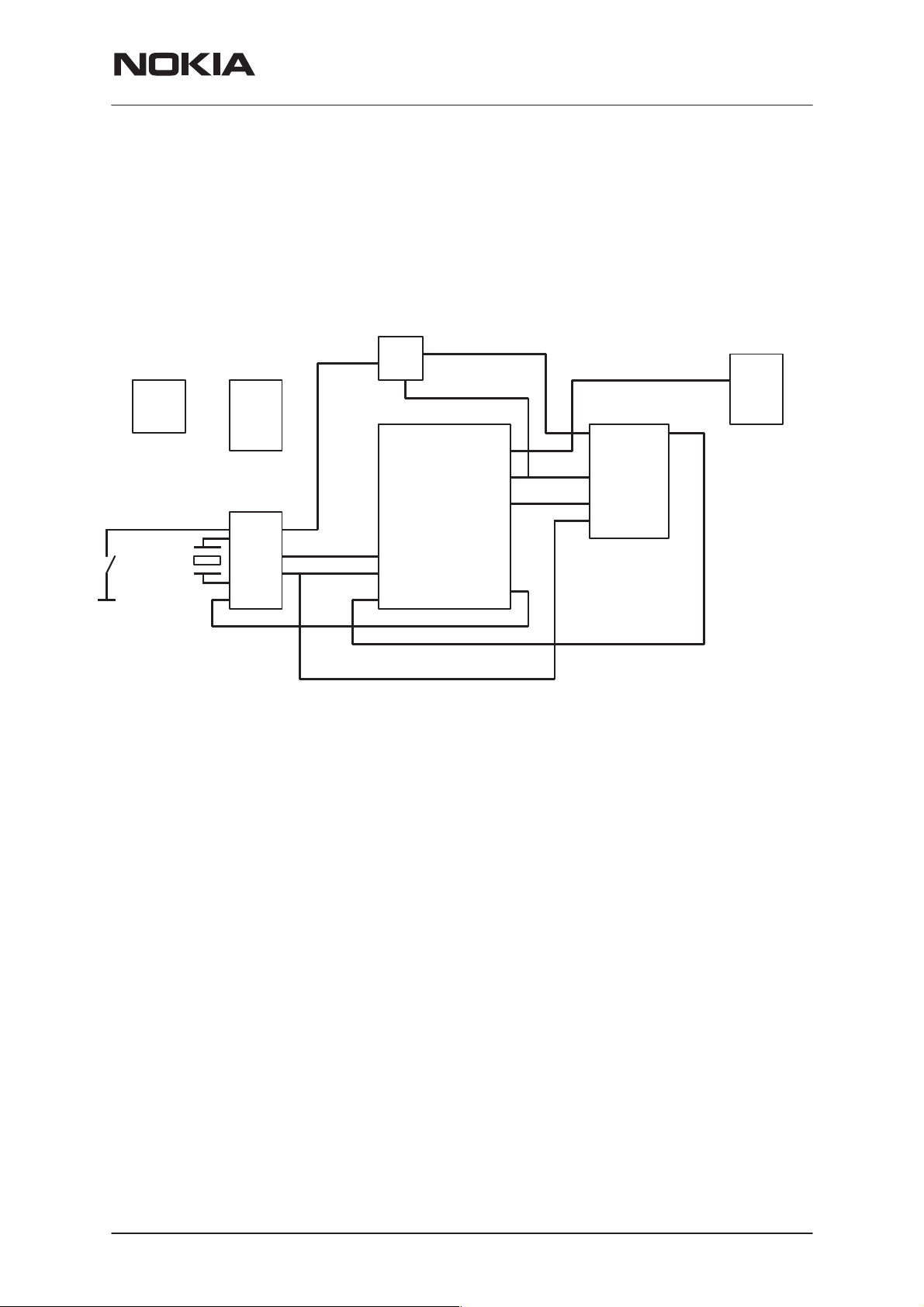
Charging Control
Charging is controlled by MCU SW, which writes control data to CCONT
via serial bus. CCONT output pin PWMOUT (Pulse Width Modulation)
can be used to control both the charger and the CHAPS circuit inside
phone.
1 (1)
NSW-6
System Module SE2
CHAPS
Vin
System
Connector
PWMOU
To
charger
T
Charging
Control
Two–wire Charging
With 2–wire charging the charger provides constant output current, and
the charging is controlled by PWMOUT signal from CCONT to CHAPS.
PWMOUT signal frequency is selected to be 1 Hz, and the charging
switch in CHAPS is pulsed on and off at this frequency. The final charged
energy to battery is controlled by adjusting the PWMOUT signal duty
cycle.
BATTERY
MAD
CCONT
serial
control
Pulse width is controlled by the MCU which writes these values to
CCONT.
Three–wire Charging
With 3–wire charging the charger provides adjustable output voltage, and
the charging is controlled by PWMOUT signal from CCONT to Charger,
Issue 1 12/99
Nokia Mobile Phones Ltd.
Page 27
Page 28

NSW-6
System Module SE2
with the charger connector signal. PWMOUT signal frequency is selected
to be 32 Hz, and the charger output voltage is controlled by adjusting the
PWMOUT signal pulse width. The charger switch in CHAPS is constantly
on in this case.
Watchdog
Both MAD and CCONT include a watchdog, and both use the 32 kHz
sleep clock. The watchdog in MAD is the primary one, and this is called
SW–watchdog. MCU has to update it regularly. If it is not updated, logic
inside MAD gives reset to MAD. After the reset, MCU can read an internal status bit to see the reason for reset, whether it was from MAD or
CCONT. The SW–watchdog delay can be set between 0 and 63 seconds
at 250 millisecond steps; and after power–up the default value is the max.
time.
PAMS Technical Documentation
VCXO
BATTERY
MAD COBBA
CCONT
32 kHz
VR1
VR6
VBB
SLCL
K
MCU
LOGIC
SIO
MAD must reset CCONT watchdog regularly. CCONT watchdog time can
be set through SIO between 0 and 63 seconds at 1 second steps. After
power–up the default value is 32 seconds. If watchdog elapses, CCONT
will cut off all supply voltages.
After total cut–off the phone can be re–started through any normal
power–up procedure.
LCD–DRVR
Battery Overvoltage Protection
Output overvoltage protection is used to protect phone from damage. This
function is also used to define the protection cutoff voltage for different
battery types (Li or Ni). The power switch is immediately turned OFF if the
voltage in VOUT rises above the selected limit VLIM1 or VLIM2.
Page 28
Nokia Mobile Phones Ltd.
Issue 1 12/99
Page 29

PAMS Technical Documentation
Parameter Symbol LIM input Min Typ Max Unit
NSW-6
System Module SE2
Output voltage cutoff limit
(during transmission or Li–
battery)
Output voltage cutoff limit
(no transmission or Ni–bat-
tery)
The voltage limit (VLIM1 or VLIM2) is selected by logic LOW or logic HIGH
on the CHAPS LIM– input pin. Default value is lower limit VLIM1.
Battery Identification
Different battery types are identified by a pulldown resistor inside the
battery pack. The BSI line inside transceiver has a 100k pullup to VBB.
The MCU can identify the battery by reading the BSI line DC–voltage level
with a CCONT A/D–converter.
VLIM1 LOW 4.4 4.6 4.8 V
VLIM2 HIGH 4.8 5.0 5.2 V
BVOLT
BATTERY
47k at
25 deg C
Vibra Schematic
BTEMP
BSI
R
s
BGND
Vbb
100k
10k
10n
TRANSCEIVER
BSI
CCONT
Issue 1 12/99
Nokia Mobile Phones Ltd.
Page 29
Page 30

NSW-6
System Module SE2
Battery Temperature
The battery temperature is measured with a NTC inside the battery pack.
The BTEMP line inside transceiver has a 100k pullup to VREF. The MCU
can calculate the battery temperature by reading the BTEMP line
DC–voltage level with a CCONT A/D–converter.
PAMS Technical Documentation
BVOLT
BATTERY
R
T
NTC
Supply Voltage Regulators
BSI
BTEMP
BGND
1k
TRANSCEIVER
VREF
Vibra Schematic
100k
10k
2k2
10n
BTEMP
VibraPWM
MCUGenIO4
CCONT
MAD
Page 30
The heart of the power distribution is the CCONT. It includes all the
voltage regulators and feeds the power to the whole system. The
baseband digital parts are powered from the VBB regulator which
provides 2.8V baseband supply. The baseband regulator is active always
when the phone is powered on. The VBB baseband regulator feeds MAD
and memories, COBBA digital parts and the LCD driver in the UI section.
VSIM supplies programming voltage to the FLASH memory. The COBBA
analog parts are powered from a dedicated 2.8V supply VCOBBA. The
CCONT supplies also 5V for RF. The CCONT features a real time clock
function, which is powered from a RTC backup when the main battery is
disconnected.
The RTC backup is rechargeable polyacene battery, which has a capacity
of 50uAh (@3V/2V) The battery is charged from the main battery voltage
Nokia Mobile Phones Ltd.
Issue 1 12/99
Page 31

PAMS Technical Documentation
by the CHAPS when the main battery voltage is over 3.2V. The charging
current is 200uA (nominal).
NSW-6
System Module SE2
Operating mode Vref RF REG VCOB-
VBB VSIM SIMIF
BA
Power off Off Off Off Off Off Pull
down
Power on On On/Off On On On On/Off
Reset On Off
VR1 On
On On Off Pull
down
Sleep On Off On On On On/Off
Note: CCONT includes also five additional 2.8V regulators providing power to the RF
section. These regulators can be controlled either by the direct control signals from MAD
or by the RF regulator control register in CCONT which MAD can update. Below are the
listed the MAD control lines and the regulators they are controlling.
–
TxPwr controls VTX regulator (VR5)
–
RxPwr controls VRX regulator (VR2)
–
SynthPwr controls VSYN_1 and VSYN_2 regulators (VR4 and VR3)
–
VCXOPwr controls VXO regulator (VR1)
CCONT generates also a 1.5 V reference voltage VREF to COBBA and
EROTUS. The VREF voltage is also used as a reference to the CCONT
A/D converter.
In addition to the above mentioned signals MAD includes also TXP control
signal which goes to PLUSSA power control block and to the power
amplifier. The transmitter power control TXC is led from COBBA to
PLUSSA.
Audio Control
The audio control and processing is taken care by the COBBA_D, which
contains the audio and RF codecs, and the MAD1, which contains the
MCU, ASIC and DSP blocks handling and processing the audio signals.
Issue 1 12/99
Nokia Mobile Phones Ltd.
Page 31
Page 32

NSW-6
System Module SE2
Slide
PAMS Technical Documentation
EMI
XMICP
XMICN
Headset
Connector
XEARP
XEARN
Display
Bias +
EMI+ACC
Interf.
EMI
EMI
MIC2
MIC1
AuxOut
Preamp
MIC3
HFCM
Amp Multipl.
HF
EAR
Multipl.Premult.
COBBA
Pre
&
LP
LP
A
D
D
A
DSP
MAD
MCU
The baseband supports three microphone inputs and two earphone
outputs. The inputs can be taken from an internal microphone, a headset
microphone or from an external microphone signal source. The
microphone signals from different sources are connected to separate
inputs at the COBBA_D asic. Inputs for the microphone signals are
differential type.
Buzzer
Driver
Circuit
Buzzer
The MIC1 inputs are used for a headset microphone that can be
connected directly to the headset connector. The internal microphone is
connected to MIC2 inputs and an external pre–amplified microphone
(handset/handfree) signal is connected to the MIC3 inputs. In COBBA
there are also three audio signal outputs of which dual ended EAR lines
are used for internal earpiece and HF line for accessory audio output. The
third audio output AUXOUT is used only for bias supply to the headset
microphone. As a difference to DCT3 generation both external MIC & EAR
are fully differential (4–wire IF). No common mode line (SGND) is used.
The output for the internal earphone is a dual ended type output capable
of driving a dynamic type speaker. Input and output signal source
selection and gain control is performed inside the COBBA_D asic
according to control messages from the MAD1. Keypad tones, DTMF, and
other audio tones are generated and encoded by the MAD1 and
transmitted to the COBBA_D for decoding.
Internal Microphone and Earpiece
The baseband supports three microphone inputs and two earphone
outputs. The inputs can be taken from an internal microphone, a headset
microphone or from an external microphone signal source. The
microphone signals from different sources are connected to separate
inputs to the COBBA_D asic. Inputs for the microphone signals are of a
differential type.
Page 32
Nokia Mobile Phones Ltd.
Issue 1 12/99
Page 33

PAMS Technical Documentation
External Audio Connections
The external audio connections are presented in the figure on the
previous page. A headset can be connected directly to the headset
connector. The headset microphone bias is supplied from COBBA
AUXOUT output and fed to microphone through XMIC line.
Audio Accessory Detection
When the MCU–SW receives a headset–interrupt, generated by the
switch in the headset–connector, it will start the accessory–detection
sequence.
At first it will measure the voltage at XMICP–pin (divided in half by 2
resistors) via EAD AD–converter in CCONT. If it detects a voltage it will
start the sequence for the active accessory detection. The only specified
active accessory for NSW–6 is the PPH–3 handsfree kit.
NSW-6
System Module SE2
If there is no active voltage detected at XMICP, AUXOUT–pin of
COBBA_D is switched to 1.5V and the voltage at XMICP is measured
again. The voltage at XMICP depends on the impedance which is
connected between XMICP and XMICN ath the accessory end.
Connector Line Symbol Minimum Typical / Nominal Unit / Notes
Connection
State
No accessory
connected
Headset HDC–5
with button not
pressed
Headset HDC–5
with button
pressed
PPH–3 (connected correctly)
PPH–3 with external microphone (connected correctly)
HOOKDET
(MAD1 pin C10)
’1’ ’0’ 0V 0
’1’ ’1’ 1.1V 390 When AUXOUT at 1.5V
’0’ ’1’ 0.75V 255 When AUXOUT at 1.5V
’0’ ’1’ 2.6V 900 when muted
’0’ ’1’ 2.2V 750 when muted
HEADSETINT
(MAD1 pin B1 1)
Voltage at
XMICP
EAD–value Notes
Audio box JBA-6
’1’ ’1’ ~0.9V 330 – 350 when AUXOUT at 1.5V
Internal Audio Connections (speech processing)
The speech coding functions are performed by the DSP in the MAD1 and
the coded speech blocks are transferred to the COBBA_D for digital to
analog conversion, down link direction. In the up link direction the PCM
coded speech blocks are read from the COBBA_D by the DSP.
Issue 1 12/99
Nokia Mobile Phones Ltd.
Page 33
Page 34

NSW-6
System Module SE2
4–wire PCM Serial Interface
The interface consists of following signals: a PCM codec master clock
(PCMDClk), a frame synchronization signal to DSP (PCMSClk), a codec
transmit data line (PCMTX) and a codec receive data line (PCMRX). The
COBBA_D generates the PCMDClk clock, which is supplied to DSP SIO.
The COBBA_D also generates the PCMSClk signal to DSP by dividing the
PCMDClk. The PCMDClk frequency is 1.000 MHz and is generated by
dividing the RFIClk 13 MHz by 13. The COBBA_D further divides the
PCMDClk by 125 to get a PCMSClk signal, 8.0 kHz.
PCMDClk
PCMSClk
PAMS Technical Documentation
PCMTxData
PCMRxData
The output for the internal earphone is a dual ended type output capable
of driving a dynamic type speaker. The output for the external accessory
and the headset is single ended with a dedicated signal ground SGND.
Input and output signal source selection and gain control is performed
inside the COBBA_D asic according to control messages from the
MAD1PR1. Keypad tones, DTMF, and other audio tones are generated
and encoded by the MAD1PR1 and transmitted to the COBBA_D for
decoding. MAD1PR1 generates two separate PWM outputs, one for a
buzzer and one for vibra (internal and external via BTEMP).
Speech Processing
The speech coding functions are performed by the DSP in the MAD1 and
the coded speech blocks are transferred to the COBBA_D for digital to
analog conversion, down link direction. In the up link direction the PCM
coded speech blocks are read from the COBBA_D by the DSP.
sign extended
15 14 13 12 011 10
sign extended
MSB
MSB
LSB
LSB
Page 34
There are two separate interfaces between the MAD and the COBBA: 2
serial buses. The first serial interface is used to transfer all the COBBA
control information (both the RFI part and the audio part). The second
serial interface between the MAD and COBBA includes transmit and
receive data, clock and frame synchronization signals. It is used to
transfer the PCM samples. The frame synchronization frequency is 8 kHz
( the sample rate is in digital mode 8.0 kHz and in analog mode 8.1 kHz)
which indicates the rate of the PCM samples and the clock frequency is 1
MHz. The COBBA is generating both clocks.
Nokia Mobile Phones Ltd.
Issue 1 12/99
Page 35

PAMS Technical Documentation
Alert Signal Generation
A buzzer is used for giving alerting tones and/or melodies as a signal of
an incoming call. Also keypress and user function response beeps are
generated with the buzzer. The buzzer is controlled with a BuzzerPWM
output signal from the MAD1. A dynamic type of buzzer is used since the
supply voltage available can not produce the required sound pressure for
a piezo type buzzer. The low impedance buzzer is connected to the
UI–switch ASIC. The alert volume can be adjusted either by changing the
pulse width causing the level to change or by changing the frequency to
utilize the resonance frequency range of the buzzer.
A vibra alerting device is used for giving a silent signal to the user of an
incoming call. The device is controlled with a Vibra output signal from the
MAD1.
NSW-6
System Module SE2
Issue 1 12/99
Nokia Mobile Phones Ltd.
Page 35
Page 36

NSW-6
System Module SE2
Digital Control
MAD
The baseband functions are controlled by the MAD asic, which consists of
a MCU, a system ASIC and a DSP.
MAD(1) contains following building blocks:
– ARM RISC processor with both 16–bit instruction set (THUMB mode)
and 32–bit instruction set (ARM mode)
– DSP core with peripherals:
– BUSC (BusController for controlling accesses from ARM to API, Sys-
tem Logic and MCU external memories, both 8– and 16–bit memories)
PAMS Technical Documentation
– API (Arm Port Interface memory) for MCU–DSP commu-
nication, DSP code download, MCU interrupt handling vec-
tors (in DSP RAM) and DSP booting
– Serial port (connection to PCM)
– Timer
– DSP memory
– System Logic
– CTSI (Clock, Timing, Sleep and Interrupt control)
– MCUIF (Interface to ARM via B
tROM
– DSPIF (Interface to DSP)
– MFI (Interface to COBBA_D AD/DA Converters)
– CODER (Block encoding/decoding and A51&A52 ciphering)
– AccIF(Accessory Interface)
– SCU (Synthesizer Control Unit for controlling 2 separate
synthesizer)
– UIF (Keyboard interface, serial control interface for COB-
BA_D PCM Codec, LCD Driver and CCONT)
– UIF+ (roller/ slide handling)
– PUP (Parallel IO, USART and PWM control unit for vibra
and buzzer)
– FLEXPOOL (DAS00308 FlexPool Specification)
– SERRFI (DAS00348 COBBA_D Specifications)
The MAD1 operates from a 13 MHz system clock, which is generated
from the 13Mhz VCXO frequency. The MAD1PR1 supplies a 6,5MHz or a
13MHz internal clock for the MCU and system logic blocks and a 13MHz
clock for the DSP, where it is multiplied to TBD MHz DSP clock. The
system clock can be stopped for a system sleep mode by disabling the
USC). Contains MCU Boo-
Page 36
Nokia Mobile Phones Ltd.
Issue 1 12/99
Page 37

PAMS Technical Documentation
VCXO supply power from the CCONT regulator output. The CCONT
provides a 32kHz sleep clock for internal use and to the MAD1PR1, which
is used for the sleep mode timing. The sleep clock is active when there is
a battery voltage available i.e. always when the battery is connected.
Memories
The MCU program code resides in an external program memory, size
is16Mbits. MCU work (data) memory size is 2Mbits (128k x16). A special
block in the flash is used for storing the system and tuning parameters,
user settings and selections, a scratch pad and a short code memory.
The BusController (BUSC) section in the MAD1 decodes the chip select
signals for the external memory devices and the system logic. BUSC
controls internal and external bus drivers and multiplexers connected to
the MCU data bus. The MCU address space is divided into access areas
with separate chip select signals. BUSC supports a programmable
number of wait states for each memory range.
NSW-6
System Module SE2
Program Memory 16MBit Flash
The MCU program code resides in the flash program memory. The
program memory size is 16Mbits (1Mx16) . The default package is
uBGA48.
SRAM Memory
The work memory size is 2Mbits (128kx16) static ram in a 48 ball BGA
package. Vcc is 2.8V and access time is 100 ns The work memory is
supplied from the common baseband VBB voltage and the memory
contents are lost when the baseband voltage is switched off. All retainable
data is stored into the flash memory when the phone is powered down.
EEPROM Emulated in FLASH Memory
A block in flash is used for a nonvolatile data memory to store the tuning
parameters and phone setup information. The short code memory for
storing user defined information is also implemented in the flash. The
EEPROM space allocated is about 32kbyte The memory is accessed
through the parallel bus.
Flash Programming
The program execution starts from the BOOT ROM and the MCU
investigates in the early start–up sequence if the flash prommer is
connected. This is done by checking the status of the MBUS–line.
Normally this line is high but when the flash prommer is connected the
line is forced low by the prommer. The flash prommer serial data receive
line is in receive mode waiting for an acknowledgement from the phone.
Issue 1 12/99
Nokia Mobile Phones Ltd.
Page 37
Page 38

NSW-6
System Module SE2
The data transmit line from the baseband to the prommer is initially high.
When the baseband has recognized the flash prommer, the FBUS TX–line
is pulled low. This acknowledgement is used to start the data transfer of
the first two bytes from the flash prommer to the baseband on the FBUS
RX–line. The data transmission begins by starting the serial transmission
clock (MBUS–line) at the prommer.
The 2.8V programming voltage is supplied inside the transceiver from the
CCONT.
The following table lists out the flash programming pads under the battery,
(holes are provided in the shield)
Name Parameter Min Typ Max Unit Remark
PAMS Technical Documentation
MBUS Serial clock
from the
Prommer
FBUS_RXSerial data
from the
Prommer
FBUS_TXData ac-
knowledge
to the
Prommer
GND GND 0 0 V Supply ground
2.0
0
2.0v
0v
2.0
0,1
2.8
0.8
2.8
0.8
2.8
0.8
V Prommer detection and Seri-
al Clock for synchronous
communication
V Receive Data from
Prommer to Baseband
V Transmit Data from Base-
band to Prommer
Page 38
Nokia Mobile Phones Ltd.
Issue 1 12/99
Page 39

PAMS Technical Documentation
RF Module
Technical Summary
The RF module converts the signal received by the antenna to a
baseband signal and vice versa.
It consists of a conventional superheterodyne receiver and a transmitter
for each band and also two frequency synthesizers for the required
mixing.
The RF module includes one integrated circuit, the EROTUS a BiCMOS
ASIC.
The dual–band RF–module is capable for seamless operation between
800 MHz and 1900 MHz bands. In practise this means capability to
cross–band hand–offs and maho–measurements.
NSW-6
System Module SE2
The EROTUS includes:
– Limiter amplifier for the analog receiver
– An AGC amplifier for the digital receiver
– A receiver mixer for the 450kHz down conversion
– PLLs for the 1GHz UHF and VHF synthesizers
– IQ–modulators for the transmitter
– A power control circuit for the transmitter and the AGC amplifier
The power amplifiers (PAs) are GaAs HBT MMICs. They comprise two
800 MHz and three 1900 MHz amplifier stages with input and interstage
matching.
The LNA MMICs include:
– A LNA for each band with a step AGC
– Down converters for the receiver
– A prescaler for the LO buffer
On the next page is a graphical presentation of the used Frequency Plan.
RF Frequency Plan
Intermediate frequencies of the RX are the same in all operation modes.
RX/TX LO and TX IF modulator frequencies are different in TDMA800
and TDMA1900 operation modes. See figure below for details.
Issue 1 12/99
Nokia Mobile Phones Ltd.
Page 39
Page 40

NSW-6
System Module SE2
PAMS Technical Documentation
1930.08–1989.96 MHz
869.04–893.97 MHz
2046.24–2106.18 MHz
LO 1
PLLLO 3
1850.01–1909.95 MHz
824.01–848.97 MHz
NOTE!
Frequencies in
TDMA1900
are printed in italics
mode
985.20–1010.16 MHz
196.23 MHz
161.19 MHz
LO 2
392.46 MHz
322.38 MHz
1st IF
116.19 MHz
PLL
f
f/2
PLL
VCTCXO
19.44 MHz
2nd IF
450 kHz
116.64 MHz
EROTUS
IF2 A–mode
450 kHz
IF2 D–mode
450 kHz
2f
f
58.32 MHz
3f
f
RFC 19.44 MHz
DC Characteristics
Power Distribution Diagram
There are two options for power distribution. 1st option is a dual band
phone, which is presented in the diagram next page. Current consumptions in the diagrams are only suggestive.
Page 40
Nokia Mobile Phones Ltd.
Issue 1 12/99
Page 41

TypeYourNameHere TypeDateHere
PAMS Technical Documentation
NSW-6
System Module SE2
RFCEN
SPWR1
TXPWR1
RXPWR1
SPWR2
(via serial bus)
TXPWR3
TXP1
VR7_bias
DUAL BAND OPERA TION
VR1
VREF
VR2
V5V
VR6
VR5
VR4
VR3
CCONT
VR7
VRBB BASEBAND
2 mA
19.44 MHz
8 mA
30 mA
1 mA
4 mA
3 mA
15 mA
Enable
3 mA
55 mA
VCTCXO
3* Multiplier
UHF–
VCO
2 mA
COBBA_D
(Analog)
Detector
VRS
IF1 –
amp.
VHF
VCO
TQ UHF
LO buffer
TX mixer
TDMA800
TX PA bias
TDMA800
TX driver
TDMA800
2 mA
2 mA
6 mA
10 mA
5 mA (peak)
2 mA
1 mA
35 mA
26 mA/ 5.6 mA
1 mA
doubler
VHF
presc.
Bias
UHF
presc.
& PLL
Phase
Digital
supply
Power
control
Modulator
Digital m.
RX IF– parts
Analog m.
IF– parts
Limiter
EROTUS
Control
block
TX PA
TDMA800
Freq.
det.
SDATA
SCLK
SENA1
VBATT
RXPWR2
RXPWR3
SPWR3
TXP2
TXPWR2
Enable
VR8
VR9
VR10
VR11
VR12
19 mA
30 mA
35 mA
Enable
RX FRONT
END TDMA800
RX FRONT
END TDMA1900
TX mixer
TDMA1900
10 mA
10 mA
Enable
3 mA
65 mA
4 mA
TX PA
TDMA1900
2GHz VCO
2GHz PLL
TX PA bias
TDMA 1900
TX driver
TDMA1900
TQ UHF
LO buffer
5 mA
Issue 1 12/99
Nokia Mobile Phones Ltd.
Page 41
Page 42

NSW-6
System Module SE2
Current consumption in different operation modes can be seen in the
table below:.
PAMS Technical Documentation
800 MHz
Ext.
Standby
[mA]
VR1 9.0 / 0.0 9.0 9.0 9.0 / 0.0 9.0 19.0 / 0.0 19.0
VR2 16.0 / 0.0 16.0 16.0 16.0 / 0.0 16.0 0.0 0.0
VR3 0.0 0.0 23.0 0.0 13.0 0.0 8.0
VR4 11.6 / 0.0 11.6 11.6 32 / 0.0 12.8* 32 / 0.0 12.8*
VR5 0.0 0.0 37.0 0.0 13.0 ** 0.0 13.0 **
VR6 2.0 / 0.1 2.0 32.0 *** 2.0 / 0.1 32.0 *** 2.0 / 0.1 32.0 ***
VR7 0.0 0.0 58.0 0.0 19.2 ’ 0.0 0.0
VR8 19.0 / 0.0 19.0 19.0 19.0 / 0.0 7.6 ’’ 0.0 0.0
VR9 0.0 0.0 0.0 0.0 0.0 30.0 / 0.0 12.0 ’’’
VR10 0.0 0.0 0.0 0.0 0.0 10.0 / 0.0 10.0
VR11 0.0 0.0 0.0 0.0 0.0 0.0 22.5^
VR12 0.0 0.0 0.0 0.0 0.0 0.0 12.9^^
V5V 5.0 / 0.0 5.0 5.0 5.0 / 0.0 5.0 5.0 / 0.0 5.0
Total 62.6 / 0.1 62.6 210.6 83.0 / 0.1 127.6 98.0 / 0.1 147.2
NOTES: * Mean value (ON/OFF=8/20ms), peak current 32.0 mA
** Mean value (ON/OFF=7/20ms), peak current 37.0 mA
*** Cobba_D mean current consumption estimated to be 30 mA
’ Mean value (ON/OFF=6.6/20ms), peak current 180.0 mA
’’ Mean value (ON/OFF=8/20ms), peak current 10.0 mA
’’’ Mean value (ON/OFF=8/20ms), peak current 15.0 mA when AGC2=1
^ Mean value (ON/OFF=6.6/20ms), peak current 68.0 mA
^^ Mean value (ON/OFF=6.6/20ms), peak current 39.0 mA
800 MHz
Analog
Control
Channel
[mA]
800 MHz
Analog
Traffic
Channel
[mA]
800 MHz
Digital
Control
Channel
[mA]
800 MHz
Digital
Traffic
Channel
[mA]
1900 MHz
Digital
Control
Channel
[mA]
1900 MHz
Digital
Traffic
Channel
[mA]
Regulators
Most of the RF voltage regulation functions are located in the regulator IC
CCONT. It has 8 separate regulators with power on/off controls (see fig
2). Regulator VR6 is used also for the COBBA_D IC and the rest of the
regulators VR1–VR7 are reserved for the RF blocks only. VR7_bias controls the 800MHz PA bias to boost better efficiency in analog mode and at
power levels 6 to 10 in digital mode. VSIM voltage is used for the PLL
charge pump supply. In dual band phone there is a need for 5 additional
regulators, which are integrated in Penta regulator IC.
Receiver
DAMPS800 RX
The receiver is a double conversion receiver. Most of the RX functions
are integrated in two ICs, namely receiver front end and EROTUS. Re-
Page 42
Nokia Mobile Phones Ltd.
Issue 1 12/99
Page 43

PAMS Technical Documentation
ceiver front end contains a LNA and the 1st mixer. Analog and digital IF–
parts are integrated in the EROTUS.
The received RF signal from the antenna is fed through a duplex filter to
the receiver unit. The signal is amplified by a low noise preamplifier. In
digital mode the gain of the amplifier is controlled by the AGC2 control
line. The nominal gain of 19 – 20 dB is reduced in the strong signal
condition about 14 – 16 dB (in digital mode). After the preamplifier the
signal is filtered with a SAW RF filter. The filter rejects spurious signals
coming from the antenna and spurious emissions coming from the mixer
and IF parts.
The filtered RF–signal is downconverted by an active mixer. The frequency of the first IF is 116.19 MHz. The first local signal is generated in
the UHF synthesizer. The IF signal is fed through a SAW IF–filter. The
filter rejects intermodulating signals and the second IF image signal. The
filtered 1st IF is fed to the receiver section of the integrated RF circuit
EROTUS, which has separate IF paths for analog and digital modes of
operation.
NSW-6
System Module SE2
In digital mode the IF1 signal is amplified by an AGC amplifier, which has
a gain control range of 57 dB. The gain is controlled by an analog signal
with AGC1–line. The amplified IF signal is down converted to a second
IF in the mixer of EROTUS. The second local signal is the 6th overtone of
the 19.44 MHz VCTCXO. LO frequency multiplier is implemented in two
stages. First multiplication by 3 is done with a EROTUS multiplier with an
external trap and the second multiplication by 2 is done in the integrated
doubler in EROTUS.
The second IF frequency is 450 kHz. The second IF is filtered by two ceramic filters. The filter rejects signals on the adjacent channels. The filtered second IF is fed back to EROTUS, where it is amplified and fed
balanced out to COBBA_D via IF2D lines.
In analog mode the filtered and amplified IF1 signal is fed to a mixer. This
mixer has been optimized for low current consumption. After this the
mixer down converted signal is fed through the same IF2 filter as in digital
mode and finally it is amplified in the limiter amplifier. The limited IF2 signal is fed via balanced IF2A lines to COBBA_D, which has a digital FM–
detector. The limiter amplifier produces also a RSSI voltage for analog
mode field strength indication.
TDMA 1900 RX
On 1900 MHz band the receiver operates only in digital mode. There is a
separate front end for this band. IF–parts are common for both bands.
Operation of the receiver is similar to digital mode operation on 800 MHz
band.
Frequency Synthesizers
The stable frequency reference for the synthesizers and base band circuits is a voltage controlled temperature compensated crystal oscillator
Issue 1 12/99
Nokia Mobile Phones Ltd.
Page 43
Page 44

NSW-6
System Module SE2
VCTCXO. Frequency of the oscillator is 19.44 MHz. It is controlled by an
AFC voltage, which is generated in the base band circuits. In digital mode
operation, the receiver is locked to base station frequency by AFC. Next
to detector diode, there is a sensor for temperature measurement. Voltage RFTEMP from this sensor is fed to baseband for A/D conversion.
This information of the RF PA–block temperature is used as input for
compensation algorithms.
The ON/OFF switching of the VCTCXO is controlled by the sleep clock in
the baseband via RFCEN. Other parts of the synthesizer section are 1
GHz VCO, 2 GHz VCO, VHF VCO, PLL for 2 GHz VCO and PLL sections
of the EROTUS IC.
DAMPS 800 operation
1GHz UHF synthesizer generates the down conversion injection for the
receiver and the up conversion injection for the transmitter. UHF frequency is 985.20 ... 1010.16 MHz, depending on the channel which is
used. 1GHz UHF VCO is a module. The PLL circuit is dual PLL, common
for both UHF and VHF synthesizers. These PLLs are included in the
EROTUS IC.
PAMS Technical Documentation
LO signal for the 2nd RX mixer is multiplied from the VCTCXO frequency
as described above.
VHF synthesizer is running only on digital or analog traffic channel.
322.38 MHz signal (divided by 2 in EROTUS) is used as a LO signal in
the I/Q modulator of the transmitter chain.
TDMA 1900 operation
2 GHz VCO with external PLL circuit generates 2046.24 ... 2106.18 MHz
injection signals for 1st RX mixer and TX upconverter.
VHF synthesizer is running only on digital traffic channel. Operating frequency 392.46 MHz is fed to EROTUS modulator, where it is divided by 2
and used as modulator LO signal.
Transmitter
DAMPS800 TX
The TX intermediate frequency is modulated by an I/Q modulator contained in the transmitter section of EROTUS IC. The TX I and TXQ signals are generated in the COBBA_D interface circuit and they are fed differentially to the modulator.
Page 44
Intermediate frequency level at the modulator output is controlled by
power control.
The output signal from EROTUS modulator is filtered to reduce harmonics and RX–band noise. The final TX signal is achieved by mixing the
Nokia Mobile Phones Ltd.
Issue 1 12/99
Page 45

PAMS Technical Documentation
UHF VCO signal and the modulated TX intermediate signal in an active
mixer. After the mixing TX signal is amplified by a driver stage. From
driver stage the signal is fed trough the TX filter to PA MMIC.
The PA amplifies the TX signal by 28–32 dB. Amplified TX signal is filtered in the duplex filter. Then signal is fed to the antenna, where the
maximum output level is typically 480 mW.
The power control loop controls the gain of the EROTUS gain control
stage. The power detector consists of a directional coupler and a diode
rectifier. The output voltage of the detector is compared to TXC voltage in
EROTUS. The power control signal (TXC), comes from the RF interface
circuit, COBBA_D. TXP signal sets driver power down to ensure off–burst
level requirements.
False transmission indication is used to protect transmitter against false
transmission caused by component failure. Protection circuit is in EROTUS. The level for TXF is set by internal resistor values in EROTUS.
NSW-6
System Module SE2
TDMA1900 TX
See 800 MHz digital mode transmitter.
DAMPS800/TDMA1900 operation
Supply voltages in different modes of operation
800
MHz
Ext.
Stadby
VR1 ON/OFF ON ON ON/OFF ON ON/OFF ON
VR2 ON/OFF ON ON ON/OFF ON ON/OFF* ON/OFF*
VR3 OFF OFF ON OFF ON OFF OFF
VR4 ON/OFF ON ON ON/OFF ON/OFF ON/OFF ON/OFF
VR5 OFF OFF ON OFF ON/OFF OFF ON/OFF
VR6 ON ON ON ON ON ON ON
VR7 OFF OFF ON OFF ON/OFF OFF OFF
VR8 ON/OFF ON ON ON/OFF ON/OFF OFF OFF
VR9 OFF OFF OFF OFF OFF ON/OFF ON/OFF
VR10 OFF OFF OFF ON/OFF* ON/OFF* ON ON
VR11 OFF OFF OFF OFF OFF OFF ON/OFF
VR12 OFF OFF OFF OFF OFF OFF ON/OFF
VSIM ON/OFF ON ON ON/OFF ON ON/OFF ON
NOTE: * ON during interband MAHO
800
MHz
Analog
Control
Channel
800
MHz
Analog
Traffic
Channel
800
MHz
Digital
Control
Channel
800
MHz
Digital
Traffic
Channel
1900
MHz
Digital
Control
Channel
1900
MHz
Digital
Traffic
Channel
Issue 1 12/99
Nokia Mobile Phones Ltd.
Page 45
Page 46

NSW-6
System Module SE2
Software Compensations
Power Levels (TXC) vs. Temperature
Because of wide temperature range, it is necessary to compensate the
effect of temperature on the output power. To monitor this environment
change, temperature measurement is done by using NTC resistor. A
Factor table is used for temperature compensation. The table values are
defined without factory measurements. Temperature is measured and
right compensation value is added to TXC–value. Requirement for compensation update is for every 1 minutes or after every 5 degrees C of
temperature change. This means that the output power is reduced linearly from level 2 to –1dB when temperature inside the phone is above +80
C in analog mode and above +65 C in digital mode.
Power Levels (TXC) vs. Channel
PAMS Technical Documentation
Duplexer frequency response ripple is compensated by software. Power
levels are calibrated on four channels in production. Values for channels
between these tuned channels are calculated using linear interpolation.
Power levels vs. Battery Voltage
To extend battery duration in digital mode, the output power is decreased
linearly from level 2 to –1dB when battery voltage drops below 3.3V.
TX Power Up/Down Ramps
Transmitter output power up/down ramps are controlled by SW. A special
ramp tables are used for that. Requirement is for nine different ramps in
digital mode for both operating bands and one ramp for analog mode.
Separate ramps are used in power up and power down ramps.
Digital Mode RSSI
Digital mode RSSI vs. input signal is calibrated in production, but RSSI
vs. temperature and RSSI vs. channel are compensated by software.
Page 46
Nokia Mobile Phones Ltd.
Issue 1 12/99
Page 47

PAMS Technical Documentation
RF Block Specifications
Receiver
DAMPS 800MHz RX Front End
Receiver front end is integrated in the IC. It has RF amplifier with a gain
step and an active mixer. RX interstage filter is a SAW filter.
NSW-6
System Module SE2
Parameter Min Typ/
Max Unit
Nom
Supply voltage 2.7 2.8 2.85 V
RF amplifier current cons. 10.0 11.0 mA
Mixer current consumption 3.0 5.0 mA
LO buffer current consumption 2.0 3.0 mA
2nd buffer current consumption 2.0 3.0 mA
RF amplifier frequency range 869 – 894 MHz
RF amplifier insertion gain 18 19 20 dB, AGC2 = H
RF amplifier gain variation ±1.0 dB, temp –30...+85 C
RF amplifier absolute gain red. 15 dB, AGC2 = L
RF amplifier noise figure 1.7 2.0 dB, AGC2 = H
RF amplifier noise figure 15 dB, AGC2 = L
RF amplifier reverse isolation 15 dB
RF amplifier IIP3 –7 –6 dBm
RF amp input VSWR 2.0 (Zo=50 ohms)
RF amp output VSWR 2.0 (Zo=50 ohms)
Mixer input frequency range 869 – 894 MHz
Mixer power gain 4 5 6 dB
Mixer NF, SSB 8 9 dB
Mixer IIP3 5 7 10 dBm
Mixer single input resistance 50 Ω
Mixer bal. output resistance 900 Ω (open collector)
LO level in mixer RF–input –3 –0 +3 dBm
Mixer RF–IF isolation 20 40 dB
LO signal frequency range 985 1011 MHz
LO input resistance 50 Ω
Value(s) based on NMP specification nr.19190
TDMA 1900MHz RX Front End
Receiver front end is integrated in the IC. It has RF amplifier with a gain
step and an active mixer. RX interstage filter is a dielectric filter.
Issue 1 12/99
Nokia Mobile Phones Ltd.
Page 47
Page 48

NSW-6
System Module SE2
PAMS Technical Documentation
Parameter Min Typ/
Max Unit
Nom
Supply voltage 2.7 2.8 2.85 V
RF amplifier current cons. 15.0 17.0 mA
Mixer current consumption 11.0 15.0 mA
RF amplifier frequency range 1930 – 1990 MHz
RF amplifier insertion gain 18 19 20 dB, AGC2 = H
RF amplifier gain variation ±1.0 dB, temp –30...+85 C
RF amplifier absolute gain red. 15 dB, AGC2 = L
RF amplifier noise figure 1.7 2.0 dB, AGC2 = H
RF amplifier noise figure 15 dB, AGC2 = L
RF amplifier reverse isolation 15 dB
RF amplifier IIP3 –7 dBm
Mixer input frequency range 1930 – 1990 MHz
Mixer power gain 4 5 6 dB
Mixer NF, SSB 8 9 dB
Mixer 1/2 IF Spurious rejection –70 –68 dBc
Mixer IIP3 5 7 10 dBm
LO level in mixer RF–input –10 –6 –4 dBm
Mixer RF–IF isolation 20 30 dB
LO signal frequency range 2046.2 2106.2 MHz
LO single ended input level 200 mVpp
LO input resistance 50 Ω
* Value(s) based on NMP specification nr.19191
SAW Filter
The 1st IF filter is a SAW filter. The function of the filter is to provide attenuation for the intermodulating signals
Analog IF parts
Analog mode IF–parts are included in EROTUS. Functional blocks: IF1
amplifier, a 2x–multiplier for LO signal, a mixer and a limiter amplifier
with RSSI. Specifications for analog mode IF–parts are in table 5. IF2
filter is a double 450 kHz ceramic filter.
Supply voltage 2.7 2.8 2.9 V
IF1 amp + mixer current cons. 6 8 mA
6x freq. multipl. current cons. 1.8 mA
Limiter + RSSI current cons. 1.3 mA
Parameter Min Typ/
Nom
Max Unit
(+0.6 mA in d–mode)
Page 48
Nokia Mobile Phones Ltd.
Issue 1 12/99
Page 49

PAMS Technical Documentation
NSW-6
System Module SE2
MinParameter
UnitMaxTyp/
Nom
Power up time 2 ms
RF input impedance single end 900//–1 kohm//pF
RF input frequency range 45 116.19 120 MHz
Noise figure, IF1 amp + mixer 8 dB, RF = 116 MHz
Conversion gain @
Rl=1.5kohm
Conversion gain variation TBD dB, temp –30...+85 C
3rd order input intercept point 20 mV
Mixer output frequency range 450 kHz
Mixer out to limiter in isolation 70 80 dB, @ 450 kHz
Limiter input frequency 450 kHz
Limiter input limiting range 30 uV
Limiter output voltage 0.3 V
Limiter output resistive load 10 kW
Limiter output capacitive load 5 pF
RSSI dynamic range 65 70 dB
RSSI starting level @ LIMIN1 30 60 uVrms
RSSI voltage slope 5 10 mV/dB
RSSI voltage range 0.1 1.5 V
RSSI output capacitive load 50 pF
RSSI output resistive load 500 kΩ
Freq. multiplier input frequency 19.44 MHz
Input signal spurious levels –8 –10 dBc, (19.44 MHz
Input signal level 50 tbd mV
25 33 dB
rms
rms
pp
spurs)
peak
Digital IF parts
The digital IF–parts of EROTUS comprise AGC Amplifer with 57 dB control range, a mixer and a buffer amplifier for the last IF.
Supply voltage 2.7 2.8 2.9 V
Current consumption 43 mA
RF input frequency range 45 116.19 120 MHz
Local frequency (6x19.44 MHz) 116.64 MHz
IF frequency 450 kHz
Max voltage gain, AGC + mixer 47 dB
Min voltage gain, AGC + mixer –10 dB
Gain change, AGC + mixer ±5 dB, temp
Issue 1 12/99
Parameter Min Typ/
Nom
Nokia Mobile Phones Ltd.
Max Unit
–30...+85 C
Page 49
Page 50

NSW-6
System Module SE2
PAMS Technical Documentation
Noise figure @ max gain 8 dB
Control voltage for min gain 0.5 V
Control voltage for max gain 1.4 1.45 V
AGC gain control slope TBD 90 TBD dB/V
Mixer output 1dB compr. point 0.8 V
Gain of the last IF buffer 34 36 38 dB, single ended
Max IF2–buffer output level 1.4 V
IF2–buffer output impedance 300 ohm, single ended
Transmitter
RF Characteristics of the transmitter:
TX frequency range 824.01...848.97 MHz 1850.01...1909.95 MHz
Type
Intermediate frequency 161.19 MHz 196.23 MHz
Nominal power on highest power level 480mW (≈ 26.8 dBm) / 400mW (≈ 26 dBm)
Power control range 65 dB
Maximum rms error vector 12.5 %
MinParameter
UnitMaxTyp/
Nom
pp
pp
Item DAMPS TDMA1900
Upconversion
TX Power levels
Power level Analog
0 28 +2 ,–4 28 +2 ,–4 28 +2 ,–4 dBm
1 28 +2 ,–4 28 +2 ,–4 28 +2 ,–4 dBm
2
Reduced 2 (*
Power level Analog
3 24 +2 ,–4 24 +2 ,–4 24 +2 ,–4 24 +2 ,–2 dBm
4 20 +2 ,–4 20 +2 ,–4 20 +2 ,–4 20 +2 ,–2 dBm
5 16 +2 ,–4 16 +2 ,–4 16 +2 ,–4 16 +2 ,–2 dBm
6 12 +2 ,–4 12 +2 ,–4 12 +2 ,–4 12 +2 ,–2 dBm
7 8 +2 ,–4 8 +2 ,–4 8 +2 ,–4 8 +2 ,–2 dBm
8 – 4 +2 ,–4 4 +2 ,–6 4 +2 ,–2 dBm
9 – 0 +2 ,–6 0 +2 ,–8 0 +2 ,–2 dBm
10 – –4 +2 ,–8 –4 +2 ,–10 –4 +2 ,–2 dBm
Digital mode
mode
Class III Class IV Class IV Class IV dBm
28 +2 ,–4
26 +2 ,–2
mode
800 MHz
28 +2 ,–4
26 +2 ,–2
Digital mode
800 MHz
Digital mode
1900 MHz
28 +2 ,–4
26 +2 ,–2
Digital mode
1900 MHz
Design
target (**
28 +0.5 ,–1
26 +1 ,–1
Design
target (**
Unit /
Notes
dBm
Unit /
Notes
Page 50
Nokia Mobile Phones Ltd.
Issue 1 12/99
Page 51

PAMS Technical Documentation
Synthesizers
UHF Synthesizers specification
NSW-6
System Module SE2
Parameter UHF 800MHz
analog mode
rx/tx injec-
tion
Frequency range 985.20 ...
1010.16
Reference frequency 30 30 30 kHz
Reference peaks @ 30 kHz
@ 60 kHz
2 x fo level –20 –20 –20 dBc
Phase noise, fo _ 60 kHz
fo _120 kHz
Phase error – 4 4
Residual FM
Filters: 300 Hz HP
3 kHz LP
Frequency settling time
within _ 3 kHz
within _ 30 Hz 20
Start up settling time 30 3 3 ms, max
–31
–70
–115
150 – – Hz, max
UHF 800MHz
digital mode
rx/tx slot
985.20 ...
1010.16
–38
–57
–101
–121
1.4
2.0
UHF
1900MHz
rx/tx slot
2046.24 ...
2106.18
–38
–57
–101
–121
1.4
2.0
Unit/
Notes
MHz
dBc, max
dBc/Hz,
max
_
, max
rms
ms, max
VHF Synthesizers specification
Parameter VHF 800MHz
Frequency range 322.38 322.38 392.46 MHz
Reference frequency 30 30 30 kHz
Reference peaks @ 30 kHz
@ 60 kHz
2 x fo level –30 –30 –30 dBc
Phase noise, fo _ 60 kHz
fo _120 kHz
Phase error 2 2 2
Frequency settling time
within _ 3 kHz
within _ 30 Hz
Start up settling time 20 20 20 ms, max
VHF 800MHz
analog mode
tx injection
–31
–66
–105 –105 –105 dBc/Hz,
20 20 20
digital mode
rx/tx slot
–41
–60
VHF
1900MHz
mode tx in-
jection
–41
–60
Unit/
Notes
dBc, max
max
_
, max
rms
ms, max
Issue 1 12/99
E Nokia Mobile Phones Ltd.
Page 51
Page 52

NSW-6
System Module SE2
Output levels
PAMS Technical Documentation
Parameter Min Typ/
2G UHF synthesizer to Lo buffer
level
resistive load
parallel capacitance
1G UHF synthesizer to TX mixer
level
impedance
VHF synthesizer to EROTUS
level
resistive load
parallel capacitance
VCTCXO 19.44 MHz
level
resistive load
parallel capacitance
VCTCXO 19.44 MHz to BB
level
resistive load
parallel capacitance
VCTCXO
3 * fo level
fo and 2xfo level
harmonic suppression
resistive load
parallel capacitance
100
1k
600
1k
200
50
–25
–25
Nom
tbd
tbd
tbd
tbd
10k
tbd
5k
tbd
Max Unit
–10 dBm
Ω
pF
–5 dBm
Ω
mV
pp
Ω
pF
mV
pp
Ω
20
100 mV
pF
mV
Ω
pF
dBc
dBc
Ω
pF
pp
pp
RF/BB interface signals
CCONT (baseband) control signals are included in table below..
control signals are printed in
Signal
name
VBAT battery RF
VREF CCON
VR1 CCON
From/
Con-
trol
T
T
/
RFCEN
To Parameter Min Typ Max Unit Function
Voltage 3.1 3.6 5.3 V Supply voltage for
2V8
regul.
Voltage during TX 3.0 3.6 5.0 V
Current 1200 mA
Erotus Voltage 1.478 1.50 1.523 V EROTUS reference
Current 10 uA
Erotus,
VCTCXO,
2GHz
PLL
Voltage 2.7 2.8 2.85 V Supply for VCTCXO,
italics.
These
discrete 2V8 regulators in dual band
phone
voltage
and Erotus VHF
prescaler, VCO and
bias,
2 GHz PLL
Page 52
Nokia Mobile Phones Ltd.
Issue 1 12/99
Page 53

PAMS Technical Documentation
NSW-6
System Module SE2
Signal
name
Con-
FunctionUnitMaxTypMinParameterToFrom/
trol
Current, tdma 800 3.0 7 9 mA
Current, tdma1900 3.0 17 19 mA
VR2 CCON
T
/
Erotus,
UHF
VCO1
Voltage 2.7 2.8 2.85 V Supply voltage for
tdma 800 UHF VCO
and prescaler
SPWR
1
Current, tdma800 14 16 20 mA
Current, tdma1900 off mA
VR3 CCON
T
/
SPWR
VHF–
VCO,
LO–buff,
TX mixer
Voltage 2.7 2.8 2.85 V Supply for VHF VCO,
LO buffer, tdma800
TX mixer and TXF
2
(via
serial
bus)
Current, tdma800 20 24 30 mA
Current, tdma1900 4 9 12 mA
VR4 CCON
T
/
Erotus,
VCTCXO
IF1–amp
Voltage 2.7 2.8 2.85 V Supply for Erotus
IF–parts, IF1–amp.,
VCTCXO multiplier
RXPW
R1
Current, anal.RX 10 12 15 mA
Current, digi.RX 30 32 34 mA
VR5 CCON
T
/
Erotus,
TX pwr
control
Voltage 2.7 2.8 2.85 V Supply for Erotus
modulator, TX pwr
control
TXPW
R1
Current, TX–mode 33 37 41 mA
VR6 CCON
T
VR7 CCON
T
TXP1
V5V CCON
T
/
Erotus
disc.PLL
Cobba_D
TX PA V oltage 2.7 2.88 2.95 V TX PA bias and TX
EROTUS Voltage 4.8 5.0 5.2 V Erotus and discrete
Voltage 2.7 2.8 2.85 V Erotus & disc PLL:
digital supply ,
Cobba_D:
analog supply
Current (RF block) 2.0 3.0 mA
driver regulator
enable
Current, tdma800 55 60 mA
synthesizer phase
det
RFCEN
Current 3.0 5.0 mA
RFTEMP RF CCONT Voltage 0 1.5 V RF temperature sen-
sor (47 k NTC to
GND)
Issue 1 12/99
Nokia Mobile Phones Ltd.
Page 53
Page 54

NSW-6
System Module SE2
PAMS Technical Documentation
Signal
name
Con-
trol
AFC Cob-
ba_D
AGC1 Cob-
ba_D
FunctionUnitMaxTypMinParameterToFrom/
VCTCXO Voltage Min 0.05 1.2 2.25 V Automatic frequency
control signal for
VCTCXO. When
DAC is switched
OFF AFC output is in
high–Z mode
Resolution 11 bits
Load resistance
(dynamic)
Load resistance
(DC)
EROTUS Voltage Min 0.5 1.40 V Digital mode receiver
Load resistance 10 kΩ
Load capacitance 10 pF
Resolution 10 bits
Timing inaccuracy 8 us
10 kΩ
110 kΩ
gain control.
DSP
AGC2 MAD
(CTID
AGC2,
genpio)
BAND
Not
in use
MODE MAD PA, (FM–
Cob-
ba_D
RX LNA Logic high ”1” 2.0 V LNA gain switch.
detector)
Polarity: 0=reduced
1=normal
DSP
Logic low ”0” 0.7 V
Sink/source curr. 20 uA
Load capacitance 10 pF
Timing inaccuracy 8 us
Logic high ”1” 2.1 V TDMA800 operation
Logic low ”0” 0 0.4 V TDMA1900 operation
Sink/source curr. 1.0 mA
DSP, MCU
Load capacitance 10 pF
Timing inaccuracy 1 ms
Logic high ”1” 2.1 V Digital 800 operation
Logic low ”0” 0 0.4 V Analog 800 operation
Page 54
Sink/source curr. 2.0 mA
Load capacitance tbd pF
Timing inaccuracy ms
Nokia Mobile Phones Ltd.
DSP
Issue 1 12/99
Page 55

PAMS Technical Documentation
NSW-6
System Module SE2
Signal
name
Con-
FunctionUnitMaxTypMinParameterToFrom/
trol
IF2AP/
IF2AN
IF2DP/
IF2DN
RFC VCTCXOCobba_D Frequency 19.44 MHz High stability clock
RFCEN
ERO-
TUS
ERO-
TUS
MAD
(CTID,
Cobba_D IF2 frequency 450 kHz Differential IF2–sig-
nal from limiter to
DEMO detector in
Cobba_D
Output level, 0.6 Vpp
Load resistance 10 kΩ
Load capacitance 5 pF
Cobba_D IF2 frequency 450 kHz Differential IF2–sig-
nal
to RX A/D–converter,
PGA = 0 dB
mVpp
signal for the locig
circuits
ON, RFC enable
CCONT,
Cobba_D
Output level 170 1400
Source imp. 600 Ω
Signal amplitude 0.2 1.0 Vpp
Load resistance 10 kΩ
Load capacitance 5 pF
Logic high ”1” 2.0 V Supply voltage VR1
RFCEN
)
Logic low ”0” 0.5 V Supply voltage VR1
OFF, RFC disable
Current 100 uA
RSSI ERO-
TUS
RXPWR1
MAD
(CTID,
LNA-
SEL)
Issue 1 12/99
MCU, DSP
timing inaccuracy 50 us
CCONT Voltage 0.1 1.5 V Analog mode
field strength
indicator voltage
Digital mode
Load resistance 1 MΩ
Load capacitance 50 pF
Voltage 0.1 V
CCONT Logic high ”1” 2.0 V Supply voltage VR4
ON
Logic low ”0” 0.5 V Supply voltage VR4
OFF
Current 100 uA DSP
timing inaccuracy 30 us
Nokia Mobile Phones Ltd.
Page 55
Page 56

NSW-6
System Module SE2
PAMS Technical Documentation
Signal
name
RXPWR21)MAD
RXPWR31)MAD
Con-
trol
(CTID,
DSP
FTC)
MUX
(CTID,
DSP
FTC)
MUX
RF block
2V8
regulator
RF block
2V8
regulator
FunctionUnitMaxTypMinParameterToFrom/
Logic high ”1” 2.0 V Supply voltage VR8
ON
Logic low ”0” 0.5 V Supply voltage VR8
OFF
Current 100 uA
DSP
timing inaccuracy 30 us
Logic high ”1” 2.0 V Supply voltage VR9
ON
Logic low ”0” 0.5 V Supply voltage VR9
OFF
Current 100 uA
DSP
timing inaccuracy 30 us
.
Page 56
Nokia Mobile Phones Ltd.
Issue 1 12/99
Page 57

NSW-6
PAMS Technical Documentation
System Module SE2
Parts Lists
Engine Module SE2 (0201320)
(EDMS V 5.6)
ITEM CODE DESCRIPTION VALUE TYPE
R113 1430726 Chip resistor 100 5 % 0.063 W 0402
R150 1430788 Chip resistor 22 k 5 % 0.063 W 0402
R151 1430690 Chip jumper 0402
R153 1419007 Chip resistor 0.22 2 % 1210
R154 1430826 Chip resistor 680 k 5 % 0.063 W 0402
R158 1620025 Res network 0w06 2x100k j 0404 0404
R159 1430832 Chip resistor 2.7 k 5 % 0.063 W 0402
R160 1620019 Res network 0w06 2x10k j 0404 0404
R161 1620025 Res network 0w06 2x100k j 0404 0404
R163 1620019 Res network 0w06 2x10k j 0404 0404
R165 1430796 Chip resistor 47 k 5 % 0.063 W 0402
R166 1825005 Chip varistor vwm14v vc30v 0805 0805
R167 1430853 Chip resistor 2.2 M 5 % 0.063 W 0402
R170 1430804 Chip resistor 100 k 5 % 0.063 W 0402
R200 1620025 Res network 0w06 2x100k j 0404 0404
R201 1620025 Res network 0w06 2x100k j 0404 0404
R202 1430770 Chip resistor 4.7 k 5 % 0.063 W 0402
R209 1430812 Chip resistor 220 k 5 % 0.063 W 0402
R210 1430770 Chip resistor 4.7 k 5 % 0.063 W 0402
R211 1430804 Chip resistor 100 k 5 % 0.063 W 0402
R212 1430796 Chip resistor 47 k 5 % 0.063 W 0402
R220 1430788 Chip resistor 22 k 5 % 0.063 W 0402
R250 1620019 Res network 0w06 2x10k j 0404 0404
R251 1430710 Chip resistor 22 5 % 0.063 W 0402
R252 1430710 Chip resistor 22 5 % 0.063 W 0402
R254 1620031 Res network 0w06 2x1k0 j 0404 0404
R255 1430770 Chip resistor 4.7 k 5 % 0.063 W 0402
R256 1620025 Res network 0w06 2x100k j 0404 0404
R257 1620025 Res network 0w06 2x100k j 0404 0404
R259 1430804 Chip resistor 100 k 5 % 0.063 W 0402
R260 1430826 Chip resistor 680 k 5 % 0.063 W 0402
R261 1430826 Chip resistor 680 k 5 % 0.063 W 0402
R262 1430812 Chip resistor 220 k 5 % 0.063 W 0402
R264 1430145 Chip resistor 100 k 1 % 0.063 W 0402
R265 1430145 Chip resistor 100 k 1 % 0.063 W 0402
R266 1430726 Chip resistor 100 5 % 0.063 W 0402
R275 1620031 Res network 0w06 2x1k0 j 0404 0404
R305 1413829 Chip resistor 10 5 % 0.1 W 0805
R306 1413829 Chip resistor 10 5 % 0.1 W 0805
R307 1413829 Chip resistor 10 5 % 0.1 W 0805
Issue 1 12/99
Nokia Mobile Phones Ltd.
Page 57
Page 58

NSW-6
System Module SE2
R308 1430726 Chip resistor 100 5 % 0.063 W 0402
R309 1430726 Chip resistor 100 5 % 0.063 W 0402
R310 1430784 Chip resistor 15 k 5 % 0.063 W 0402
R311 1430784 Chip resistor 15 k 5 % 0.063 W 0402
R312 1430796 Chip resistor 47 k 5 % 0.063 W 0402
R313 1430812 Chip resistor 220 k 5 % 0.063 W 0402
R314 1430796 Chip resistor 47 k 5 % 0.063 W 0402
R331 1620031 Res network 0w06 2x1k0 j 0404 0404
R332 1430754 Chip resistor 1.0 k 5 % 0.063 W 0402
R333 1620031 Res network 0w06 2x1k0 j 0404 0404
R335 1620031 Res network 0w06 2x1k0 j 0404 0404
R337 1620031 Res network 0w06 2x1k0 j 0404 0404
R339 1620031 Res network 0w06 2x1k0 j 0404 0404
R701 1430710 Chip resistor 22 5 % 0.063 W 0402
R721 1430718 Chip resistor 47 5 % 0.063 W 0402
R725 1430710 Chip resistor 22 5 % 0.063 W 0402
R744 1430758 Chip resistor 1.5 k 5 % 0.063 W 0402
R750 1430690 Chip jumper 0402
R751 1430790 Chip resistor 27 k 5 % 0.063 W 0402
R752 1430744 Chip resistor 470 5 % 0.063 W 0402
R756 1430790 Chip resistor 27 k 5 % 0.063 W 0402
R758 1430778 Chip resistor 10 k 5 % 0.063 W 0402
R760 1620047 Res network 0w03 4x4k7 j 0804 0804
R761 1430812 Chip resistor 220 k 5 % 0.063 W 0402
R762 1430851 Chip resistor 15 k 2 % 0.063 W 0402
R763 1430758 Chip resistor 1.5 k 5 % 0.063 W 0402
R764 1430744 Chip resistor 470 5 % 0.063 W 0402
R765 1430744 Chip resistor 470 5 % 0.063 W 0402
R767 1430770 Chip resistor 4.7 k 5 % 0.063 W 0402
R768 1430778 Chip resistor 10 k 5 % 0.063 W 0402
R770 1430700 Chip resistor 10 5 % 0.063 W 0402
R771 1430700 Chip resistor 10 5 % 0.063 W 0402
R774 1430764 Chip resistor 3.3 k 5 % 0.063 W 0402
R775 1430804 Chip resistor 100 k 5 % 0.063 W 0402
R779 1430762 Chip resistor 2.2 k 5 % 0.063 W 0402
R781 1430762 Chip resistor 2.2 k 5 % 0.063 W 0402
R782 1430762 Chip resistor 2.2 k 5 % 0.063 W 0402
R786 1430726 Chip resistor 100 5 % 0.063 W 0402
R788 1430748 Chip resistor 680 5 % 0.063 W 0402
R789 1430748 Chip resistor 680 5 % 0.063 W 0402
R795 1430726 Chip resistor 100 5 % 0.063 W 0402
R796 1430700 Chip resistor 10 5 % 0.063 W 0402
R798 1430778 Chip resistor 10 k 5 % 0.063 W 0402
R801 1430754 Chip resistor 1.0 k 5 % 0.063 W 0402
R802 1430754 Chip resistor 1.0 k 5 % 0.063 W 0402
R803 1430754 Chip resistor 1.0 k 5 % 0.063 W 0402
R820 1430700 Chip resistor 10 5 % 0.063 W 0402
R821 1430726 Chip resistor 100 5 % 0.063 W 0402
PAMS Technical Documentation
Page 58
Nokia Mobile Phones Ltd.
Issue 1 12/99
Page 59

NSW-6
PAMS Technical Documentation
R822 1430754 Chip resistor 1.0 k 5 % 0.063 W 0402
R823 1430726 Chip resistor 100 5 % 0.063 W 0402
R824 1430792 Chip resistor 33 k 5 % 0.063 W 0402
R850 1430700 Chip resistor 10 5 % 0.063 W 0402
R851 1430778 Chip resistor 10 k 5 % 0.063 W 0402
R852 1430690 Chip jumper 0402
R870 1430700 Chip resistor 10 5 % 0.063 W 0402
R871 1430772 Chip resistor 5.6 k 5 % 0.063 W 0402
R872 1430700 Chip resistor 10 5 % 0.063 W 0402
R880 1430700 Chip resistor 10 5 % 0.063 W 0402
R881 1430700 Chip resistor 10 5 % 0.063 W 0402
R883 1430764 Chip resistor 3.3 k 5 % 0.063 W 0402
R884 1430726 Chip resistor 100 5 % 0.063 W 0402
R885 1430778 Chip resistor 10 k 5 % 0.063 W 0402
R900 1430718 Chip resistor 47 5 % 0.063 W 0402
R901 1430754 Chip resistor 1.0 k 5 % 0.063 W 0402
R902 1430690 Chip jumper 0402
R903 1430718 Chip resistor 47 5 % 0.063 W 0402
R904 1430690 Chip jumper 0402
R905 1430832 Chip resistor 2.7 k 5 % 0.063 W 0402
R906 1430732 Chip resistor 180 5 % 0.063 W 0402
R907 1430690 Chip jumper 0402
R925 1430718 Chip resistor 47 5 % 0.063 W 0402
R926 1430718 Chip resistor 47 5 % 0.063 W 0402
R933 1430718 Chip resistor 47 5 % 0.063 W 0402
R934 1620101 Res network 0w06 2x470r j 0404 0404
R936 1430754 Chip resistor 1.0 k 5 % 0.063 W 0402
R937 1430770 Chip resistor 4.7 k 5 % 0.063 W 0402
R938 1430784 Chip resistor 15 k 5 % 0.063 W 0402
R939 1430770 Chip resistor 4.7 k 5 % 0.063 W 0402
R940 1800659 NTC resistor 47 k 10 % 0.12 W 0805
R941 1430718 Chip resistor 47 5 % 0.063 W 0402
R942 1430762 Chip resistor 2.2 k 5 % 0.063 W 0402
R943 1430744 Chip resistor 470 5 % 0.063 W 0402
R944 1430770 Chip resistor 4.7 k 5 % 0.063 W 0402
R945 1430754 Chip resistor 1.0 k 5 % 0.063 W 0402
R961 1430690 Chip jumper 0402
R980 1430740 Chip resistor 330 5 % 0.063 W 0402
R984 1430732 Chip resistor 180 5 % 0.063 W 0402
R990 1430690 Chip jumper 0402
C100 2320560 Ceramic cap. 100 p 5 % 50 V 0402
C101 2320560 Ceramic cap. 100 p 5 % 50 V 0402
C102 2320560 Ceramic cap. 100 p 5 % 50 V 0402
C112 2320544 Ceramic cap. 22 p 5 % 50 V 0402
C151 2320544 Ceramic cap. 22 p 5 % 50 V 0402
C152 2320778 Ceramic cap. 10 n 10 % 16 V 0402
C153 2320778 Ceramic cap. 10 n 10 % 16 V 0402
C154 2320548 Ceramic cap. 33 p 5 % 50 V 0402
System Module SE2
Issue 1 12/99
Nokia Mobile Phones Ltd.
Page 59
Page 60

NSW-6
System Module SE2
C155 2320540 Ceramic cap. 15 p 5 % 50 V 0402
C157 2320778 Ceramic cap. 10 n 10 % 16 V 0402
C158 2320481 Ceramic cap. 5R 1 u 10 % 0603
C159 2320481 Ceramic cap. 5R 1 u 10 % 0603
C160 2320481 Ceramic cap. 5R 1 u 10 % 0603
C161 2320481 Ceramic cap. 5R 1 u 10 % 0603
C162 2320481 Ceramic cap. 5R 1 u 10 % 0603
C163 2320481 Ceramic cap. 5R 1 u 10 % 0603
C164 2320481 Ceramic cap. 5R 1 u 10 % 0603
C165 2320778 Ceramic cap. 10 n 10 % 16 V 0402
C166 2320481 Ceramic cap. 5R 1 u 10 % 0603
C167 2320778 Ceramic cap. 10 n 10 % 16 V 0402
C168 2320778 Ceramic cap. 10 n 10 % 16 V 0402
C169 2320481 Ceramic cap. 5R 1 u 10 % 0603
C170 2320481 Ceramic cap. 5R 1 u 10 % 0603
C171 2320584 Ceramic cap. 1.0 n 5 % 50 V 0402
C175 2312405 Ceramic cap. 2.2 u 10 % 10 V 1206
C176 2320469 Ceramic cap. Y5 V 0603
C179 2310791 Ceramic cap. 33 n 20 % 50 V 0805
C180 2312401 Ceramic cap. 1.0 u 10 % 10 V 0805
C181 2320783 Ceramic cap. 33 n 10 % 10 V 0402
C184 2320744 Ceramic cap. 1.0 n 10 % 50 V 0402
C185 2611727 Tantalum cap. 15 u 20 % 10 V
3.2x1.6x1.6
C186 2610029 Tantalum cap. 10 u 20 % 10 V
3.5x2.8x1.2
C187 2320481 Ceramic cap. 5R 1 u 10 % 0603
C189 2320481 Ceramic cap. 5R 1 u 10 % 0603
C190 2320629 Ceramic cap. 50 V 0402
C192 2610029 Tantalum cap. 10 u 20 % 10 V
3.5x2.8x1.2
C200 2320805 Ceramic cap. 100 n 10 % 10 V 0402
C201 2320481 Ceramic cap. 5R 1 u 10 % 0603
C202 2320779 Ceramic cap. 100 n 10 % 16 V 0603
C203 2320481 Ceramic cap. 5R 1 u 10 % 0603
C210 2320783 Ceramic cap. 33 n 10 % 10 V 0402
C214 2320481 Ceramic cap. 5R 1 u 10 % 0603
C217 2320481 Ceramic cap. 5R 1 u 10 % 0603
C218 2320481 Ceramic cap. 5R 1 u 10 % 0603
C219 2320481 Ceramic cap. 5R 1 u 10 % 0603
C220 2320805 Ceramic cap. 100 n 10 % 10 V 0402
C221 2320805 Ceramic cap. 100 n 10 % 10 V 0402
C225 2320481 Ceramic cap. 5R 1 u 10 % 0603
C255 2320783 Ceramic cap. 33 n 10 % 10 V 0402
C256 2320783 Ceramic cap. 33 n 10 % 10 V 0402
C257 2610029 Tantalum cap. 10 u 20 % 10 V
3.5x2.8x1.2
C258 2320805 Ceramic cap. 100 n 10 % 10 V 0402
PAMS Technical Documentation
Page 60
Nokia Mobile Phones Ltd.
Issue 1 12/99
Page 61

NSW-6
PAMS Technical Documentation
C259 2312295 Ceramic cap. Y5 V 1206
C260 2312295 Ceramic cap. Y5 V 1206
C263 2320805 Ceramic cap. 100 n 10 % 10 V 0402
C264 2320805 Ceramic cap. 100 n 10 % 10 V 0402
C265 2320805 Ceramic cap. 100 n 10 % 10 V 0402
C266 2320805 Ceramic cap. 100 n 10 % 10 V 0402
C274 2320805 Ceramic cap. 100 n 10 % 10 V 0402
C275 2320805 Ceramic cap. 100 n 10 % 10 V 0402
C276 2320805 Ceramic cap. 100 n 10 % 10 V 0402
C277 2320805 Ceramic cap. 100 n 10 % 10 V 0402
C285 2320783 Ceramic cap. 33 n 10 % 10 V 0402
C286 2320481 Ceramic cap. 5R 1 u 10 % 0603
C303 2320544 Ceramic cap. 22 p 5 % 50 V 0402
C304 2320544 Ceramic cap. 22 p 5 % 50 V 0402
C305 2320544 Ceramic cap. 22 p 5 % 50 V 0402
C306 2320544 Ceramic cap. 22 p 5 % 50 V 0402
C307 2320544 Ceramic cap. 22 p 5 % 50 V 0402
C330 2320560 Ceramic cap. 100 p 5 % 50 V 0402
C331 2320560 Ceramic cap. 100 p 5 % 50 V 0402
C332 2320560 Ceramic cap. 100 p 5 % 50 V 0402
C333 2320560 Ceramic cap. 100 p 5 % 50 V 0402
C334 2320560 Ceramic cap. 100 p 5 % 50 V 0402
C335 2320560 Ceramic cap. 100 p 5 % 50 V 0402
C336 2320560 Ceramic cap. 100 p 5 % 50 V 0402
C337 2320560 Ceramic cap. 100 p 5 % 50 V 0402
C338 2320560 Ceramic cap. 100 p 5 % 50 V 0402
C339 2320560 Ceramic cap. 100 p 5 % 50 V 0402
C340 2320560 Ceramic cap. 100 p 5 % 50 V 0402
C341 2320560 Ceramic cap. 100 p 5 % 50 V 0402
C343 2320805 Ceramic cap. 100 n 10 % 10 V 0402
C344 2320805 Ceramic cap. 100 n 10 % 10 V 0402
C701 2320629 Ceramic cap. 50 V 0402
C703 2320552 Ceramic cap. 47 p 5 % 50 V 0402
C705 2320592 Ceramic cap. 2.2 n 5 % 50 V 0402
C706 2320552 Ceramic cap. 47 p 5 % 50 V 0402
C707 2320522 Ceramic cap. 2.7 p 0.25 % 50 V 0402
C708 2320520 Ceramic cap. 2.2 p 0.25 % 50 V 0402
C709 2320552 Ceramic cap. 47 p 5 % 50 V 0402
C710 2320620 Ceramic cap. 10 n 5 % 16 V 0402
C713 2320560 Ceramic cap. 100 p 5 % 50 V 0402
C715 2320540 Ceramic cap. 15 p 5 % 50 V 0402
C716 2320524 Ceramic cap. 3.3 p 0.25 % 50 V 0402
C717 2320612 Ceramic cap. 50 V 0402
C719 2320618 Ceramic cap. 4.7 n 5 % 25 V 0402
C720 2320618 Ceramic cap. 4.7 n 5 % 25 V 0402
C721 2320560 Ceramic cap. 100 p 5 % 50 V 0402
C729 2320620 Ceramic cap. 10 n 5 % 16 V 0402
C733 2320536 Ceramic cap. 10 p 5 % 50 V 0402
System Module SE2
Issue 1 12/99
Nokia Mobile Phones Ltd.
Page 61
Page 62

NSW-6
System Module SE2
C734 2320536 Ceramic cap. 10 p 5 % 50 V 0402
C735 2320520 Ceramic cap. 2.2 p 0.25 % 50 V 0402
C736 2320524 Ceramic cap. 3.3 p 0.25 % 50 V 0402
C739 2320522 Ceramic cap. 2.7 p 0.25 % 50 V 0402
C742 2320560 Ceramic cap. 100 p 5 % 50 V 0402
C743 2320552 Ceramic cap. 47 p 5 % 50 V 0402
C744 2320514 Ceramic cap. 1.2 p 0.25 % 50 V 0402
C745 2320617 Ceramic cap. 30 p 2 % 50 V 0402
C746 2320560 Ceramic cap. 100 p 5 % 50 V 0402
C748 2320620 Ceramic cap. 10 n 5 % 16 V 0402
C749 2320560 Ceramic cap. 100 p 5 % 50 V 0402
C750 2320584 Ceramic cap. 1.0 n 5 % 50 V 0402
C751 2320584 Ceramic cap. 1.0 n 5 % 50 V 0402
C755 2320568 Ceramic cap. 220 p 5 % 50 V 0402
C756 2320620 Ceramic cap. 10 n 5 % 16 V 0402
C757 2320576 Ceramic cap. 470 p 5 % 50 V 0402
C758 2320576 Ceramic cap. 470 p 5 % 50 V 0402
C759 2320783 Ceramic cap. 33 n 10 % 10 V 0402
C760 2320560 Ceramic cap. 100 p 5 % 50 V 0402
C761 2320618 Ceramic cap. 4.7 n 5 % 25 V 0402
C762 2320618 Ceramic cap. 4.7 n 5 % 25 V 0402
C763 2320618 Ceramic cap. 4.7 n 5 % 25 V 0402
C764 2320584 Ceramic cap. 1.0 n 5 % 50 V 0402
C765 2320584 Ceramic cap. 1.0 n 5 % 50 V 0402
C766 2320592 Ceramic cap. 2.2 n 5 % 50 V 0402
C767 2320618 Ceramic cap. 4.7 n 5 % 25 V 0402
C768 2320618 Ceramic cap. 4.7 n 5 % 25 V 0402
C769 2320620 Ceramic cap. 10 n 5 % 16 V 0402
C770 2320620 Ceramic cap. 10 n 5 % 16 V 0402
C772 2312401 Ceramic cap. 1.0 u 10 % 10 V 0805
C773 2320618 Ceramic cap. 4.7 n 5 % 25 V 0402
C779 2320620 Ceramic cap. 10 n 5 % 16 V 0402
C780 2320586 Ceramic cap. 1.2 n 5 % 50 V 0402
C781 2320620 Ceramic cap. 10 n 5 % 16 V 0402
C782 2312401 Ceramic cap. 1.0 u 10 % 10 V 0805
C783 2320620 Ceramic cap. 10 n 5 % 16 V 0402
C784 2320620 Ceramic cap. 10 n 5 % 16 V 0402
C785 2320552 Ceramic cap. 47 p 5 % 50 V 0402
C786 2320620 Ceramic cap. 10 n 5 % 16 V 0402
C787 2320564 Ceramic cap. 150 p 5 % 50 V 0402
C788 2320560 Ceramic cap. 100 p 5 % 50 V 0402
C789 2320592 Ceramic cap. 2.2 n 5 % 50 V 0402
C790 2320805 Ceramic cap. 100 n 10 % 10 V 0402
C791 2320805 Ceramic cap. 100 n 10 % 10 V 0402
C792 2320805 Ceramic cap. 100 n 10 % 10 V 0402
C793 2320805 Ceramic cap. 100 n 10 % 10 V 0402
C794 2320481 Ceramic cap. 5R 1 u 10 % 0603
C795 2320805 Ceramic cap. 100 n 10 % 10 V 0402
PAMS Technical Documentation
Page 62
Nokia Mobile Phones Ltd.
Issue 1 12/99
Page 63

NSW-6
PAMS Technical Documentation
C796 2312401 Ceramic cap. 1.0 u 10 % 10 V 0805
C797 2312401 Ceramic cap. 1.0 u 10 % 10 V 0805
C798 2320805 Ceramic cap. 100 n 10 % 10 V 0402
C799 2320536 Ceramic cap. 10 p 5 % 50 V 0402
C820 2310793 Ceramic cap. 2.2 u 10 % 10 V 0805
C821 2320560 Ceramic cap. 100 p 5 % 50 V 0402
C822 2320584 Ceramic cap. 1.0 n 5 % 50 V 0402
C823 2320564 Ceramic cap. 150 p 5 % 50 V 0402
C824 2320564 Ceramic cap. 150 p 5 % 50 V 0402
C825 2320526 Ceramic cap. 3.9 p 0.25 % 50 V 0402
C826 2310248 Ceramic cap. 4.7 n 5 % 50 V 1206
C827 2320536 Ceramic cap. 10 p 5 % 50 V 0402
C828 2310793 Ceramic cap. 2.2 u 10 % 10 V 0805
C850 2312401 Ceramic cap. 1.0 u 10 % 10 V 0805
C851 2320584 Ceramic cap. 1.0 n 5 % 50 V 0402
C854 2320584 Ceramic cap. 1.0 n 5 % 50 V 0402
C855 2320805 Ceramic cap. 100 n 10 % 10 V 0402
C870 2320584 Ceramic cap. 1.0 n 5 % 50 V 0402
C871 2320584 Ceramic cap. 1.0 n 5 % 50 V 0402
C872 2320584 Ceramic cap. 1.0 n 5 % 50 V 0402
C873 2312401 Ceramic cap. 1.0 u 10 % 10 V 0805
C874 2312401 Ceramic cap. 1.0 u 10 % 10 V 0805
C875 2320560 Ceramic cap. 100 p 5 % 50 V 0402
C880 2312401 Ceramic cap. 1.0 u 10 % 10 V 0805
C881 2320560 Ceramic cap. 100 p 5 % 50 V 0402
C882 2320520 Ceramic cap. 2.2 p 0.25 % 50 V 0402
C883 2320584 Ceramic cap. 1.0 n 5 % 50 V 0402
C884 2320584 Ceramic cap. 1.0 n 5 % 50 V 0402
C885 2320564 Ceramic cap. 150 p 5 % 50 V 0402
C886 2320564 Ceramic cap. 150 p 5 % 50 V 0402
C887 2420017 Ceramic cap. 18 n 5 % 16 V 1206
C888 2320536 Ceramic cap. 10 p 5 % 50 V 0402
C889 2320530 Ceramic cap. 5.6 p 0.25 % 50 V 0402
C890 2320520 Ceramic cap. 2.2 p 0.25 % 50 V 0402
C902 2320560 Ceramic cap. 100 p 5 % 50 V 0402
C903 2320560 Ceramic cap. 100 p 5 % 50 V 0402
C904 2320560 Ceramic cap. 100 p 5 % 50 V 0402
C905 2320620 Ceramic cap. 10 n 5 % 16 V 0402
C906 2320524 Ceramic cap. 3.3 p 0.25 % 50 V 0402
C907 2320584 Ceramic cap. 1.0 n 5 % 50 V 0402
C908 2320552 Ceramic cap. 47 p 5 % 50 V 0402
C909 2320552 Ceramic cap. 47 p 5 % 50 V 0402
C910 2320552 Ceramic cap. 47 p 5 % 50 V 0402
C912 2320805 Ceramic cap. 100 n 10 % 10 V 0402
C913 2320552 Ceramic cap. 47 p 5 % 50 V 0402
C914 2312401 Ceramic cap. 1.0 u 10 % 10 V 0805
C915 2320552 Ceramic cap. 47 p 5 % 50 V 0402
C917 2320921 Ceramic cap. 3.9 p 5 % 16 V 0402
System Module SE2
Issue 1 12/99
Nokia Mobile Phones Ltd.
Page 63
Page 64

NSW-6
System Module SE2
C918 2320939 Ceramic cap. 16 V 0402
C919 2320921 Ceramic cap. 3.9 p 5 % 16 V 0402
C920 2320536 Ceramic cap. 10 p 5 % 50 V 0402
C921 2320552 Ceramic cap. 47 p 5 % 50 V 0402
C922 2320552 Ceramic cap. 47 p 5 % 50 V 0402
C923 2320530 Ceramic cap. 5.6 p 0.25 % 50 V 0402
C931 2320520 Ceramic cap. 2.2 p 0.25 % 50 V 0402
C932 2320629 Ceramic cap. 50 V 0402
C934 2320552 Ceramic cap. 47 p 5 % 50 V 0402
C937 2320552 Ceramic cap. 47 p 5 % 50 V 0402
C938 2320536 Ceramic cap. 10 p 5 % 50 V 0402
C939 2320552 Ceramic cap. 47 p 5 % 50 V 0402
C941 2320544 Ceramic cap. 22 p 5 % 50 V 0402
C943 2320552 Ceramic cap. 47 p 5 % 50 V 0402
C949 2320522 Ceramic cap. 2.7 p 0.25 % 50 V 0402
C950 2320536 Ceramic cap. 10 p 5 % 50 V 0402
C951 2320584 Ceramic cap. 1.0 n 5 % 50 V 0402
C952 2320536 Ceramic cap. 10 p 5 % 50 V 0402
C953 2320536 Ceramic cap. 10 p 5 % 50 V 0402
C960 2312401 Ceramic cap. 1.0 u 10 % 10 V 0805
C961 2320560 Ceramic cap. 100 p 5 % 50 V 0402
C962 2320544 Ceramic cap. 22 p 5 % 50 V 0402
C963 2320481 Ceramic cap. 5R 1 u 10 % 0603
C965 2320903 Ceramic cap. 2.7 p 5 % 16 V 0402
C966 2320903 Ceramic cap. 2.7 p 5 % 16 V 0402
C967 2320532 Ceramic cap. 6.8 p 0.25 % 50 V 0402
C968 2320536 Ceramic cap. 10 p 5 % 50 V 0402
C969 2320805 Ceramic cap. 100 n 10 % 10 V 0402
C981 2320520 Ceramic cap. 2.2 p 0.25 % 50 V 0402
C982 2320560 Ceramic cap. 100 p 5 % 50 V 0402
C983 2320536 Ceramic cap. 10 p 5 % 50 V 0402
C984 2320536 Ceramic cap. 10 p 5 % 50 V 0402
L701 3645213 Chip coil 22 n 5 % Q=38/250 MHz
0603
L702 3643039 Chip coil 220 n 5 % Q=35/100 MHz
0805
L703 3645241 Chip coil 12 n 5 % Q=35/250 MHz
0603
L705 3641626 Chip coil 220 n 2 % Q=50/250 MHz
0805
L721 3645249 Chip coil 3 n 5 % Q=22/250 MHz
0603
L723 3645157 Chip coil 100 n 10 % Q=12/100 MHz
0603
L724 3640701 Chip coil 470 n 5 % Q=32/100 MHz
1008
L740 3645231 Chip coil 39 n 5 % Q=40/250 MHz
0603
PAMS Technical Documentation
Page 64
Nokia Mobile Phones Ltd.
Issue 1 12/99
Page 65

NSW-6
PAMS Technical Documentation
L741 3645301 Chip coil 180 n 5 % Q=13/100 MHz
0603
L745 3645231 Chip coil 39 n 5 % Q=40/250 MHz
0603
L747 3645231 Chip coil 39 n 5 % Q=40/250 MHz
0603
L750 3641421 Chip coil 100 u 5 % Q=15/0.796M
1008
L761 3645029 Chip coil 10 % Q=45/10 MHz
0805
L762 3641626 Chip coil 220 n 2 % Q=50/250 MHz
0805
L820 3646053 Chip coil 4 n Q=28/800M 0402
L850 3641421 Chip coil 100 u 5 % Q=15/0.796M
1008
L880 3645155 Chip coil 2 n Q=32/800M 0603
L902 3646069 Chip coil 33 n 5 % Q=23/800 MHz
0402
L903 3646069 Chip coil 33 n 5 % Q=23/800 MHz
0402
L904 3646083 Chip coil 100 n 5 % Q=16/300 MHz
0402
L905 3646083 Chip coil 100 n 5 % Q=16/300 MHz
0402
L906 3643073 Chip coil 6 n 1.4 A Q=35 0805
L908 3646083 Chip coil 100 n 5 % Q=16/300 MHz
0402
L911 3640081 Dir.coupler 836.5+–12.5mhz 1206 1206
L930 3646085 Chip coil 6 n 10 % Q=29/800 MHz
0402
L931 3646083 Chip coil 100 n 5 % Q=16/300 MHz
0402
L940 3646063 Chip coil 22 n 5 % Q=28/800 MHz
0402
L941 3646053 Chip coil 4 n Q=28/800M 0402
L951 3646069 Chip coil 33 n 5 % Q=23/800 MHz
0402
L960 3646085 Chip coil 6 n 10 % Q=29/800 MHz
0402
L961 3646043 Chip coil 1 n Q=33/800M 0402
L962 3646069 Chip coil 33 n 5 % Q=23/800 MHz
0402
L964 3643073 Chip coil 6 n 1.4 A Q=35 0805
L966 4551003 Dir.coupler 1880+–30mhz 1 4DB
L975 3645157 Chip coil 100 n 10 % Q=12/100 MHz
0603
L981 3646069 Chip coil 33 n 5 % Q=23/800 MHz
0402
System Module SE2
Issue 1 12/99
Nokia Mobile Phones Ltd.
Page 65
Page 66

NSW-6
System Module SE2
B151 4510219 Crystal 32.768 k +–30PPM 9PF
B301 5140087 Buzzer 85db 2600hz 3.6v 10x10x3. 10x10x3.5
G850 4510249 VCTCXO 19.44 M +–2.5PPM 2.8V
TDMA
G880 4350161 Vco 985.2–1010.2mhz 2.8v 10ma
G881 4350159 Vco 2046–2106mhz 2.8v 11ma
F150 5119019 SM, fuse f 1.5a 32v 0603
Z300 3640035 Filt z>450r/100m 0r7max 0.2a 0603 0603
Z301 3640035 Filt z>450r/100m 0r7max 0.2a 0603 0603
Z303 3640035 Filt z>450r/100m 0r7max 0.2a 0603 0603
Z304 3640035 Filt z>450r/100m 0r7max 0.2a 0603 0603
Z701 4511125 Saw filter 881.5+–12.5 M /4DB 3X3
Z726 4511113 Saw filter 1960+–30 M /5DB 3X3
Z741 4511011 Saw filter 116.19+–0.015 M 9.3X5
Z750 4550085 Cer.filt 450+–11.5khz/8db 6.7x5.7 6.7x5.7
Z751 4550081 Cer.filt 450+–11.5khz/8db 6.7x5.7 6.7x5.7
Z791 3640085 Filt 470nf 16v 0r03 2a 0805 0805
Z900 4511111 Dual saw filt 161/196mhz 5.2x4.7 5.2x4.7
Z901 4511123 Saw filter 836.5+–12.5 M /3.8DB 3X3
Z910 4512091 Dupl 824–849/869–894mhz 9.5x7.5
Z920 3640085 Filt 470nf 16v 0r03 2a 0805 0805
Z950 4511023 Saw filter 1880+–30 M /4.2DB 3X3
Z960 4512121 Dupl 1850–1910/1930–1990mhz 17x8 17X8
Z970 4550065 Dipl 824–894/1850–1990mhz 3.2x1.6 3.2x1.6
Z975 4511023 Saw filter 1880+–30 M /4.2DB 3X3
V100 4110067 Schottky diode MBR0520L 20 V 0.5 A SOD123
V101 4110067 Schottky diode MBR0520L 20 V 0.5 A SOD123
V102 4113671 Tvs quad 6v1 esda6v1w5 sot323–5 SOT323–5
V110 4113611 Emifilt/tvs emif01–10005w5 sot353 SOT353
V150 4210037 Transistor BCW30 pnp 32 V 0.1 A
SOT23
V151 4110067 Schottky diode MBR0520L 20 V 0.5 A SOD123
V152 4210043 Transistor DTC143ZE npn RB V EM3
V153 4211202 DM MosFet p–ch 50 V 0.13 A
SOT23
V154 4210043 Transistor DTC143ZE npn RB V EM3
V250 4210119 Transistor BC849CW npn 30 V 0.1 A
SOT323
V251 4219904 Transistor x 2 UMX1 npn 40 V SOT363
V252 4113611 Emifilt/tvs emif01–10005w5 sot353 SOT353
V301 4113671 Tvs quad 6v1 esda6v1w5 sot323–5 SOT323–5
V302 4113671 Tvs quad 6v1 esda6v1w5 sot323–5 SOT323–5
V320 4860005 Led Green 0603
V321 4860005 Led Green 0603
V322 4860005 Led Green 0603
V323 4860005 Led Green 0603
V324 4860005 Led Green 0603
V325 4860005 Led Green 0603
PAMS Technical Documentation
Page 66
Nokia Mobile Phones Ltd.
Issue 1 12/99
Page 67

NSW-6
PAMS Technical Documentation
V336 4110601 Diode FAST SOD323
V723 4110911 Cap. diode MA2SV01 1/3 V SOD523
V901 4210043 Transistor DTC143ZE npn RB V EM3
V902 4210043 Transistor DTC143ZE npn RB V EM3
V929 4110008 Schottky diode HSMS2825 8 V SOT143
V930 4110008 Schottky diode HSMS2825 8 V SOT143
V931 4112443 Pin diode BAR64–03W 200 V 0.1 A SOD323
V932 4112443 Pin diode BAR64–03W 200 V 0.1 A SOD323
D200 4340615 IC, SRAM CSP48
D201 4340585 IC, flash mem. UBGA48
D202 4370559 Mad1 v18 rom6 f731575 c07 UBGA144
N150 4370631 Ccont2i’ wfd163ke64t/8 lfbga 8X8
N151 4370621 Chaps v2.0 u423v20g36t lbga6x6
N250 4370603 Cobba_d b06 twl91302ggv UBGA64
N310 4370433 Uiswitch sttm23av20t TSSOP20
N700 4370571 Erotus 1g wfd170cg80t 80lbga 80LBGA
N701 4370063 Sc3918 tdma rec 869–894mhz QSOP16
N702 4340247 IC, regulator MC33765 2.8 V TSSOP16
N721 4370065 Sc3919 tdma rec 1930–1990 QSOP16
N770 4340233 Mrfic0916 rf amp 2500mhz sot143 SOT143
N870 4340237 IC, PLL UMA1021M SSOP20
N900 4340171 IC, upconv 1.9ghz 3v souPC8106T SO6S
N902 4340577 IC, RF amp. 21DB/900MHZ SMM6
N903 4370615 Rf9130e3 pw amp 824–849mhz tdma
N951 4340577 IC, RF amp. 21DB/900MHZ SMM6
N960 4370617 Rf9131e4 pw amp tdma1900
N980 4340381 Mrfic1813 upconvgaas 1.9g TSSOP16
S100 5219015 SM, sw push button spst 5v s.key
S330 5219005 IC, SWsp–no 30vdc 50ma SW TACT SMD
S331 5219005 IC, SWsp–no 30vdc 50ma SW TACT SMD
S332 5219005 IC, SWsp–no 30vdc 50ma SW TACT SMD
X303 5469081 SM, conn 2x7m p0.5 spr.50v PCB/PCB
I001 9380753 Bar code label dmd03311 27x6.5
9854340 PC board SE2 99.9x42.4x0.97 m8 4/pa
System Module SE2
Issue 1 12/99
Nokia Mobile Phones Ltd.
Page 67
Page 68

NSW-6
System Module SE2
PAMS Technical Documentation
This page intentionally left blank.
Page 68
Nokia Mobile Phones Ltd.
Issue 1 12/99
 Loading...