

Page 1

PAMS Technical Documentation
NSW-6 Series Transceivers
Disassembly &
Troubleshooting
Issue 1 12/99 Nokia Mobile Phones Ltd.
Page 2
NSW-6
Disassembly & Troubleshooting
AMENDMENT RECORD SHEET
PAMS Technical Documentation
Amendment
Number
Date Inserted By Comments
12/99 OJuntune New disassembly
Page 2
Nokia Mobile Phones Ltd.
Issue 1 12/99
Page 3

PAMS Technical Documentation
Disassembly & Troubleshooting
CONTENTS
Disassembly 5. . . . . . . . . . . . . . . . . . . . . . . . . . . . . . . . . . . . . . . . . . .
Baseband Testing 11. . . . . . . . . . . . . . . . . . . . . . . . . . . . . . . . . . . . . . .
Alignments 11. . . . . . . . . . . . . . . . . . . . . . . . . . . . . . . . . . . . . . . . . .
Trouble Shooting 12. . . . . . . . . . . . . . . . . . . . . . . . . . . . . . . . . . . . . . .
Phone is totally dead 13. . . . . . . . . . . . . . . . . . . . . . . . . . . . . . . . . .
Flash programming doesn’t work 14. . . . . . . . . . . . . . . . . . . . . . .
Power doesn’t stay on or the Phone is jammed 15. . . . . . . . . . .
The phone doesn’t register to the network or
phone doesn’t make a call 16. . . . . . . . . . . . . . . . . . . . . . . . . . . . .
Charging failure 18. . . . . . . . . . . . . . . . . . . . . . . . . . . . . . . . . . . . . .
RF Troubleshooting 19. . . . . . . . . . . . . . . . . . . . . . . . . . . . . . . . . . . . .
NSW-6
Page No
Introduction 19. . . . . . . . . . . . . . . . . . . . . . . . . . . . . . . . . . . . . . . . . .
Abbreviations used 20. . . . . . . . . . . . . . . . . . . . . . . . . . . . . . . . .
Interface signals between RF and BB/DSP 21. . . . . . . . . . . . . . .
Receiver 25. . . . . . . . . . . . . . . . . . . . . . . . . . . . . . . . . . . . . . . . . . . .
General instructions for RX troubleshooting 25. . . . . . . . . . . . . .
Path of the received signal 25. . . . . . . . . . . . . . . . . . . . . . . . . . . . .
AMPS RX 25. . . . . . . . . . . . . . . . . . . . . . . . . . . . . . . . . . . . . . . . .
TDMA800RX 27. . . . . . . . . . . . . . . . . . . . . . . . . . . . . . . . . . . . . .
TDMA 1900RX 30. . . . . . . . . . . . . . . . . . . . . . . . . . . . . . . . . . . .
Transmitter 32. . . . . . . . . . . . . . . . . . . . . . . . . . . . . . . . . . . . . . . . . . . . .
General Instructions for TX Troubleshooting 32. . . . . . . . . . .
Path of the transmitted signal 34. . . . . . . . . . . . . . . . . . . . . . . .
Troubleshooting diagrams for TX 35. . . . . . . . . . . . . . . . . . . . . . .
AMPS TX 35. . . . . . . . . . . . . . . . . . . . . . . . . . . . . . . . . . . . . . . . .
TDMA800 TX 37. . . . . . . . . . . . . . . . . . . . . . . . . . . . . . . . . . . . . .
TDMA1900 TX 38. . . . . . . . . . . . . . . . . . . . . . . . . . . . . . . . . . . . .
Power control loop 40. . . . . . . . . . . . . . . . . . . . . . . . . . . . . . . . .
Synthesizers 41. . . . . . . . . . . . . . . . . . . . . . . . . . . . . . . . . . . . . .
19.44 MHz Reference oscillator 41. . . . . . . . . . . . . . . . . . . . . .
58.32 MHz Triple Multiplier 41. . . . . . . . . . . . . . . . . . . . . . . . . .
19.44 MHz oscillator 42. . . . . . . . . . . . . . . . . . . . . . . . . . . . . . . .
VHF VCO 44. . . . . . . . . . . . . . . . . . . . . . . . . . . . . . . . . . . . . . . . .
AMPS& TDMA800 UHF SYNTHESIZER 45. . . . . . . . . . . . . .
TDMA1900 UHF SYNTHESIZER 46. . . . . . . . . . . . . . . . . . . . .
RF ASIC DATA 47. . . . . . . . . . . . . . . . . . . . . . . . . . . . . . . . . . . . . . .
General Info 47. . . . . . . . . . . . . . . . . . . . . . . . . . . . . . . . . . . . . . .
EROTUS ASIC 47. . . . . . . . . . . . . . . . . . . . . . . . . . . . . . . . . . . .
RX Front ends N701 and N721 47. . . . . . . . . . . . . . . . . . . . . .
Power Amplifiers N903 & N960 48. . . . . . . . . . . . . . . . . . . . . .
Issue 1 12/99
Nokia Mobile Phones Ltd.
Page 3
Page 4

NSW-6
Disassembly & Troubleshooting
PENTA regulator N702 49. . . . . . . . . . . . . . . . . . . . . . . . . . . . . .
TDMA1900 UPCONVERTER N980 49. . . . . . . . . . . . . . . . . . .
TDMA1900 PLL–circuit N870 50. . . . . . . . . . . . . . . . . . . . . . . .
Warranty transfer 51. . . . . . . . . . . . . . . . . . . . . . . . . . . . . . . . . . . . . . .
PAMS Technical Documentation
Page 4
Nokia Mobile Phones Ltd.
Issue 1 12/99
Page 5
PAMS Technical Documentation
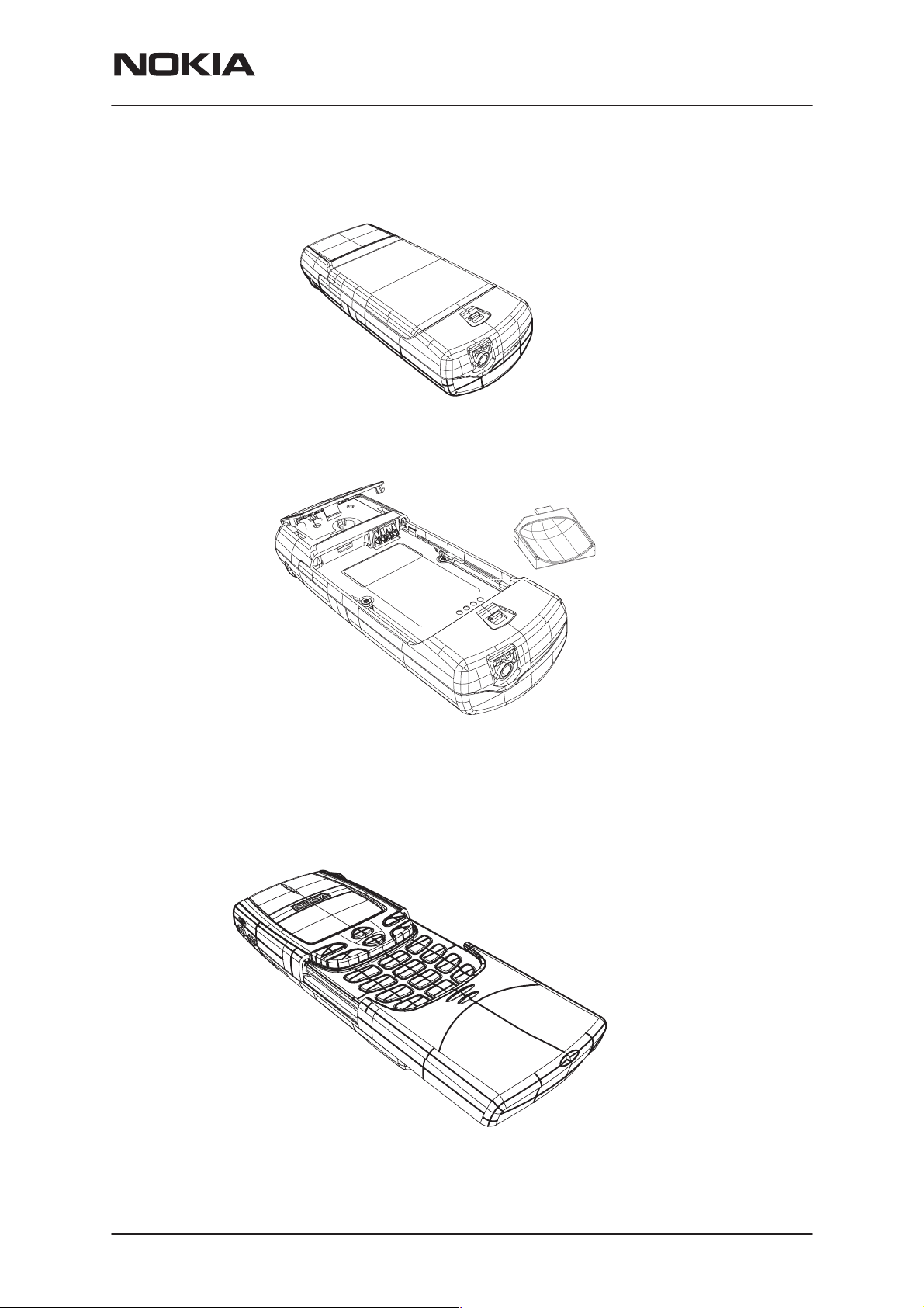
Disassembly
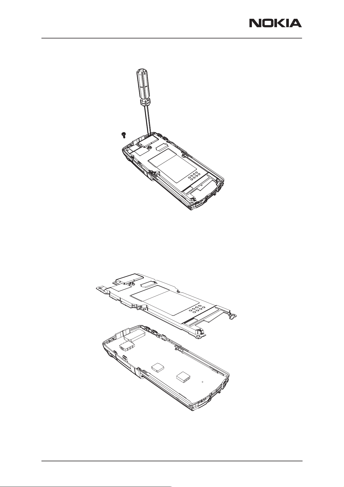
1. Remove battery
NSW-6
Disassembly & Troubleshooting
2. Remove the antenna cover by using the ART–5 antenna removal tool.
Place the ART–5 flat side down in the battery recess of the phone in the
top left hand corner. The extruding ”finger” slides in the hole next to the
battery springs and when pushing the tool the antenna is released for removal
3.Remove slide: open it halfway down, and with the left side first, remove
it by flipping it over its axle.
Issue 1 12/99
Nokia Mobile Phones Ltd.
Page 5
Page 6
NSW-6
Disassembly & Troubleshooting
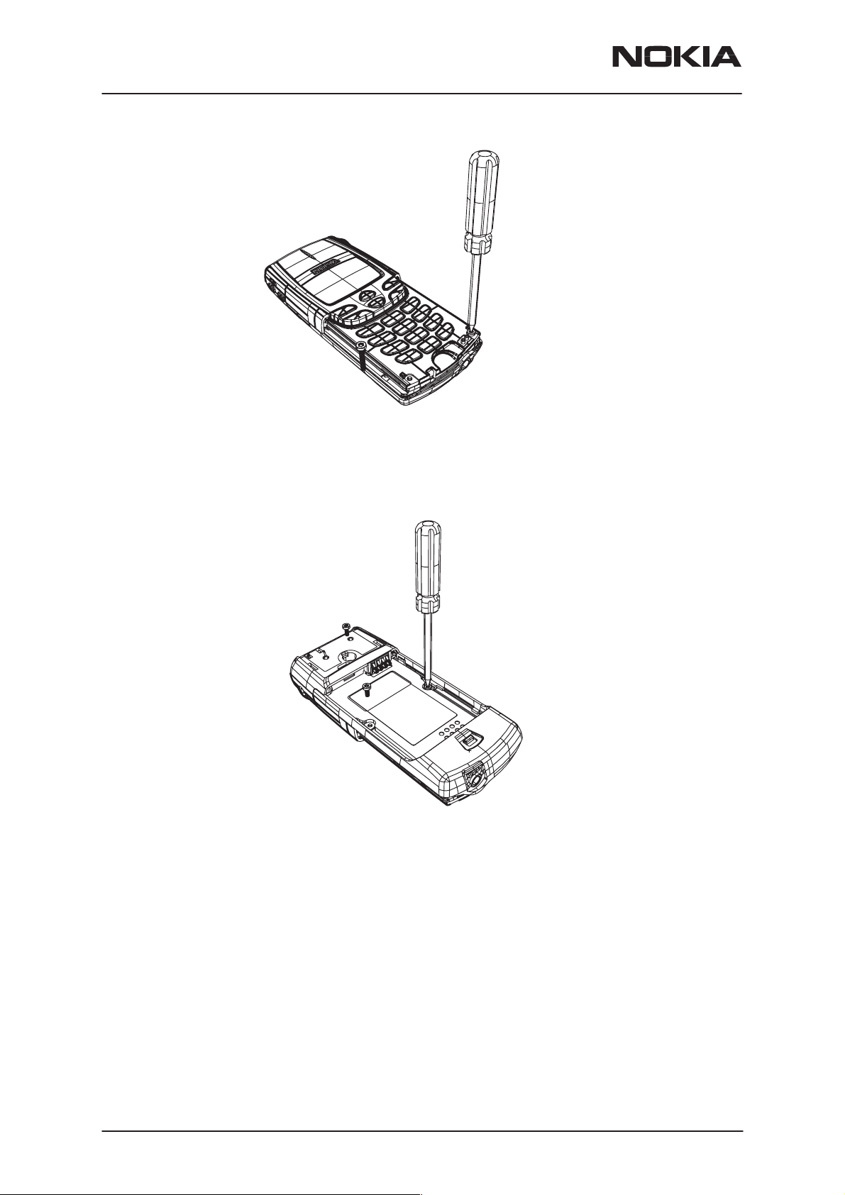
4.Remove A–cover screws (2 pcs)
PAMS Technical Documentation
Page 6
5. Turn the phone over and remove C–cover screws (3 pcs)
Nokia Mobile Phones Ltd.
Issue 1 12/99
Page 7
PAMS Technical Documentation
Snap
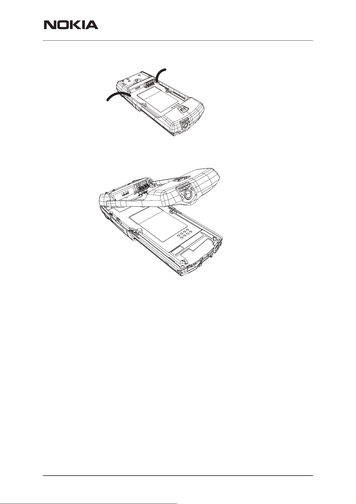
6.Release C–cover snaps
NSW-6
Disassembly & Troubleshooting
Snap
7. Open covers
Issue 1 12/99
Nokia Mobile Phones Ltd.
Page 7
Page 8
NSW-6
Disassembly & Troubleshooting
PAMS Technical Documentation
8. Remove shield screws (2 pcs)
Page 8
9. Remove shield
Nokia Mobile Phones Ltd.
Issue 1 12/99
Page 9
PAMS Technical Documentation
NSW-6
Disassembly & Troubleshooting
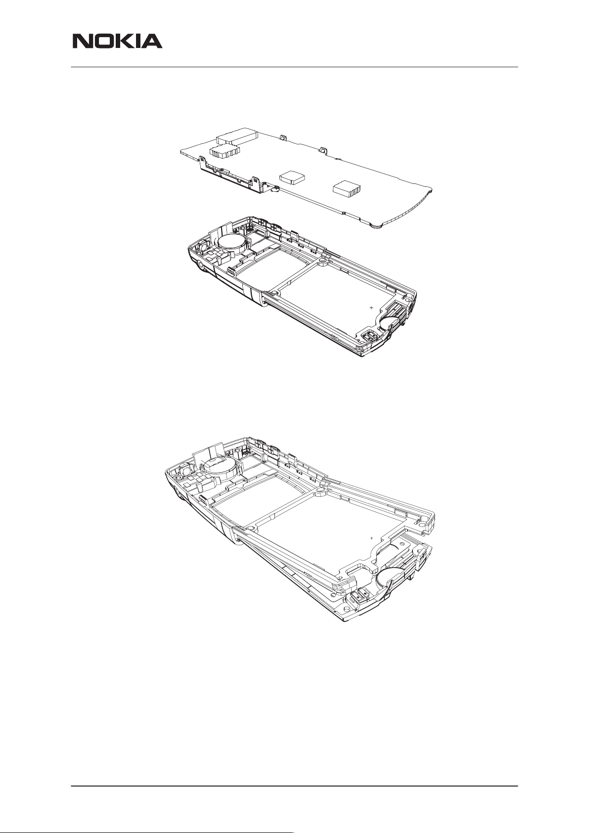
10. Remove main PCB
11. Remove slide frame, UI PCB follows
Issue 1 12/99
Nokia Mobile Phones Ltd.
Page 9
Page 10
NSW-6
Disassembly & Troubleshooting
PAMS Technical Documentation
12. Now parts can be separated from the cover.
Page 10
Nokia Mobile Phones Ltd.
Issue 1 12/99
Page 11

PAMS Technical Documentation
Baseband Testing
The MCU software enters a local mode at start-up if suitable resistors are
connected to the BTEMP and BSI lines.
NOTE! Baseband doesn’t wake up automatically when the battery voltage
is connected. Power must be switched on via:
1. Pwr key or
2. BTEMP line or
3. Charger
4. Connecting J150 to ground
Alignments
NSW-6
Disassembly & Troubleshooting
Within alignment those parameters are adjusted, that cannot be set accurate enough by design, because of component tolerances.
Due to use of 5% resistor values, the channels of the CCONT A/D converters need to be aligned in the production phase.
Within battery voltage tuning VBAT the MCU software reads the A/D reading from CCONT at 4.1 V and stores this reading to EEPROM (emulated
by Flash) memory as a reference point. Then second reading is done at
3.1 V. Now the slope is known and A/D readings can be calibrated. Calibration is included in VBAT A/D reading task.
Battery charging voltage VCHAR and current ICHAR are calibrated using
one test setting. Test jig in production line must have a connection to battery terminals. ICHAR is adjusted to 500 mA and VCHAR to 8.4 V with
appropriate load connected to the battery terminals.
Issue 1 12/99
Nokia Mobile Phones Ltd.
Page 11
Page 12

NSW-6
Disassembly & Troubleshooting
Trouble Shooting
The following hints should facility finding the cause of the problem when
the circuitry seems to be faulty. This trouble shooting instruction is divided following section.
1. Phone is totally dead
2. Flash programming does not work
3. Power does not stay on or the phone is jammed
4. Display information: Contact Service
5. Phone does not register to the network or phone does not make a call.
6. Audio fault.
7. Charging fault
The first thing to do is carry out a through visual check of the module. En-
sure in particular that:
a) there are not any mechanical damages
b) soldered joints are OK
PAMS Technical Documentation
Page 12
Nokia Mobile Phones Ltd.
Issue 1 12/99
Page 13
PAMS Technical Documentation
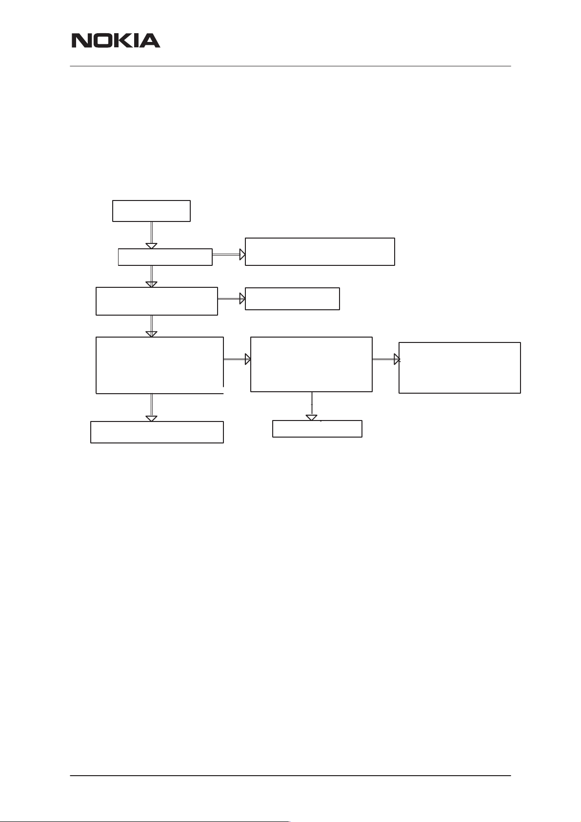
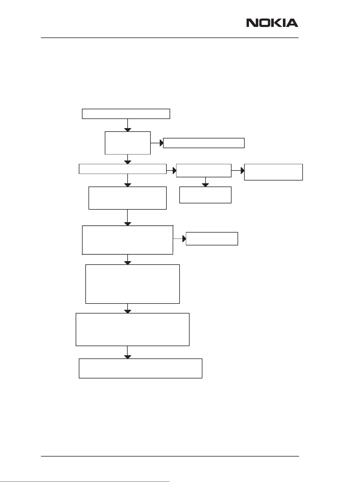
Phone is totally dead
This means that phone doesn’t take current at all when the power switch
is pressed or when the watchdog disable pin (X101 pin 11 or J150) is
grounded. Used battery voltage must be higher than 3.0 V. Otherwise the
hardware of CCONT (N150) prevents totally switching power on. Here the
VBat is set to 3.6V
Phone is
totally dead
YES
NO
VBat=3.6V at R153
YES
NSW-6
Disassembly & Troubleshooting
Failure in VBat line,
check X100
Voltage at J150 of CCONT
(N150) = 3.6V
YES
C166 (VBB) = 2.8V
C158 (VR1) = 2.8V
when PWR switch pressed or
watchdog disable pin
grounded
YES
See section: Power does not
stay on
NO
Faulty circuit N150
NO
CCONT(N150) J150 = 0V
when PWR switch pressed
or watchdog disable pin
(X101 pin 1 1) grounded
YES
Faulty circuit N160
NO
Check R160, PWR switch,
connector X300
Check watchdog disable
line X101
Issue 1 12/99
Nokia Mobile Phones Ltd.
Page 13
Page 14
NSW-6
Disassembly & Troubleshooting
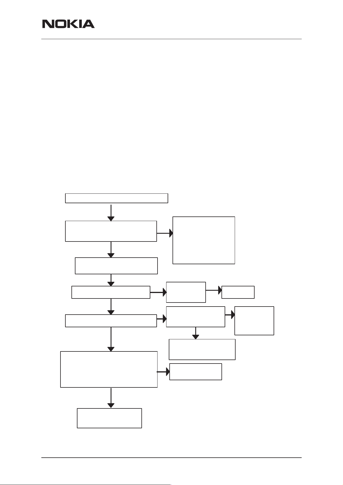
Flash programming doesn’t work
The flash programming is carried out via the pads accessible from the
back of the phone (using service accessories).
Flash programming doesn’t work
YES
PAMS Technical Documentation
VBAT > 3.0 V
VBB (C166) 2.8 V
VR1 (C158) 2.8 V
YES
PURX (J140) master reset=”1”(2.8V)
FLASH (D201) VBB is 2.8V (C203),
SRAM (D200) VBB is 2.8 V (C200),
FLASH VPP is > 2.8 V (C202)
YES
RFC (J250) 19.44 MHz sine wave
Clock signal: 700mV Vpp typ.
COBBACLK (J210) 9.72MHz sq.wave
clock signal 2.80 Vpp
OK
Check the following lines:
FBUSTXD line: J114–>MAD1
FBUSRXD line: J113–>MAD1
M2BUS line: J112 to MAD1
Check also pullup and pulldown resistors
R209, R210, R212
NO
See section ”Phone is totally dead”
NO
Sleep clock SLCLK (J157)
square wave 32 kHZ
Faulty circuit N150
or over loaded PurX line
NO
YESYES
check
VCXO G850
NO
Check sleepclock circuitry
C154, C155, C190
Page 14
OK
Check control lines of SRAM and FLASH:
e.g. there is voltage spikes when trying to write
and read something to SRAM and FLASH
RAMSelX (J207), RPMSelX (J208)
MCURDX and MCUWRX (X200 pins 19 and 18)
OK
There could be open pins in circuits D200, D201, D202
(open joints may be detectable with microscope).
If not the PCB or D202, D200, D201, N150 is faulty
Nokia Mobile Phones Ltd.
Issue 1 12/99
Page 15
PAMS Technical Documentation
Disassembly & Troubleshooting
Power doesn’t stay on or the Phone is jammed
If this kind of fault has come after flash programming, there are most
probably open pins in ICs. The solder joints of ICs: MAD1 (D202), Flash
(D201) and SRAM (D200) are to be checked at the extent possible (by
microscope from the side of PCB and lightly pressing components while
switching power on).
Normally the power will be switched off by CCONT (N150) after 32 seconds, if the watch-dog of the CCONT can not be served by software. The
watch-dog updating can be seen by oscilloscope at J154 (DataselX) of
CCONT. In normal case there is a short pulse from ”1” –> 0 every 8 seconds. The power off function of CCONT can be prevented by connecting
a short circuit wire from WDDISX (CCONT E4 (J150)) to ground (J151).
NSW-6
Power doesn’t stay on or phone is jammed
YES
CCONT (N150) watchdog is served?
J154 pulses 1 –> 0)
Connect short circuit wire from
Watchdog J150 to ground J151
OK
FLASH (D201) VBB is 2.8V (C203)
YES
PURX (J152) master reset = ”1” (2.8 V)
YES
RFC (J255) 19.44 MHz sine wave
Clock signal: 700 mV Vpp typ.
COBBACLK (J210) 9.72 MHz square wave
clock signal 2.80 Vpp
YES
YES
NO
NO
NO
Software is able to run
If power is switched off
after few seconds, check
BSI (X100 to C167) and
BTEMP (X100 to C168)
lines
YES
VBAT is OK =
3.8V
Sleep clock SLCLK
square wave 32 kHz
YES
Faulty circuit N150
or over loaded PURX line
Check VCXO G850
N150 is faulty
NO
check sleep
clock circuitry
(B150, R157...)
Issue 1 12/99
Open pins or faulty circuit:
D202, D200, D201, N150
Nokia Mobile Phones Ltd.
Page 15
Page 16

NSW-6
Disassembly & Troubleshooting
PAMS Technical Documentation
The phone doesn’t register to the network or phone
doesn’t make a call
If the phone doesn’t register to the network or the phone doesn’t make a
call, the reason could be either the baseband or the RF part. The phone
can be set to wanted mode by WinTesla service software and determinate
if the fault is in RF or in baseband part (RF interface measurements).
The control lines for RF part are supplied both the System Asic (MAD
D202) and the RFI (Cobba N250). MAD handles digital control lines and
Cobba handles analog control lines.
Diagram is on the next page.
Page 16
Nokia Mobile Phones Ltd.
Issue 1 12/99
Page 17

PAMS Technical Documentation
Phone doesn’t register to the network
or phone doesn’t make a call
YES
Analog supply voltage VR6 is > 2.7 V of
Cobba (N250) at C275
YES
Analog reference voltage Vref is 1.5
of Cobba (N250) at C169
YES
RX: VR1 (C158), VR2 (C159), VR3 (C160), VR4 (C161),
VR5 (C162), VR8 (N702 pin 14), VR9 (N702 pin 13),
TX: VR3 (C160), VR7 (C164), VR7_bias (R901),
Check supply voltages for RF:
VR10 (N702 pin 12) and V5V (C176)
VR11 (N702 pin 11), VR12 (N702 pin 9) and
TXPWR3 (C903)
YES
NO
NO
Check
N250
Check
R256
NO
NSW-6
Disassembly & Troubleshooting
Check
CCONT N150
MAD D202
Synthesizer lines: SENA2 (N880 pin 13)
SCLK (N880 pin 11)
SDATA (N880 pin 12)
pulses 0 –> 1 during off burst
YES
AGC1 (R758) 0 –> 2.3V max. during receiving burst
AFC (R850) 0 –> 1.2V typ. During receiving burst
YES
Digital data signal IF2AN (R789) –>0.6Vpp, 0–>2.2V DC
Digital data signal IF2AP (R788) –>0.6Vpp, 0–>2.2V DC
Digital data signal IF2DN (C750) –>170 mVpp typ, 0–>2.7V DC
Digital data signal IF2DP (C751) –>170 mVpp typ, 0–>2.7V DC
Frequency is 450MHz
YES
DAX signal (J211) pulses1–>0 during receiving slot
YES
TX control lines:
TXC (N750 pin 1, R752) 0 –> 2.3 Vmax during transmit burst
TXA (N750 pin 2, R751) goes 0–>1 (2.8 V) during modulation
TXLX1 (R934 pin 1) and TXLX2 (R934 pin 2) 0–> 1 (2.8 V)
YES
Analog data signals : TXIN 0–>0.8V DC during transmit slot
TXIP 0–>0.8V DC during transmit slot
TXQN 0–>0.8V DC during transmit slot
TXQP 0–>0.8V DC during transmit slot
Used
max, frequency is 12 kHz max
NO
MAD
D202
NO
NO
COBBA
N250
Check COBBA N250 if DC
fails
NO
Check RF–part if analog
signal fails
Check
N250
Check COBBA N250
if TXC fails
NO
Check MAD D202 if
TXA fails
NO
Check
N250
Check
YES
RF–part
Issue 1 12/99
Nokia Mobile Phones Ltd.
Page 17
Page 18

NSW-6
Disassembly & Troubleshooting
Charging failure
Nothing happens when charger is connected
Voltage level at VCHAR–pin of CCONT is
higher than 0.17 V
when charger is connected
Check N150
Display Information: Not charging
YES
YES
YES
PAMS Technical Documentation
NO
Check
X102, R158, R160,
F150
Voltage level at C165 is about 0.8 V when
power is connected BSI resistor value
should be 18 k
YES
Voltage level at C168 is about 0.5 V when
power is connected BTEMP resistor value
should be 47 k
YES
32 Hz square wave frequency at R150 if ACP–9U
charger is connected, 1 Hz square wave frequency if
ACP–7U or ACP–8 is connected
YES
Voltage levels at R153 are same as VBAT (C180)
YES
Voltage levels at R153 rises when
charger is connected
NO
NO
NO
NO
NO
Faulty
N151
Check
R158, R163
Check
R163, R161
Check
N150
Check
R153, N151
Page 18
Nokia Mobile Phones Ltd.
Issue 1 12/99
Page 19

PAMS Technical Documentation
RF Troubleshooting
Introduction
Measurements are done using a spectrum analyzer and a high–frequency probe (Local and reference frequencies and RF–power levels in intermediate stages of TX/RX–chains). An oscilloscope is used to measure
DC–voltages and low frequency signals. A multimeter is also a useful
measurement instrument in fault finding.
An external RF connector is assembled only on R&D– and calibration
panels for FLALI improving reliability of the measurement results, and it
should be in use when it is possible. Later on soldering pads for this connector will be removed from the layout, therefore a connector to the antenna pad needs to be soldered manually.
NSW-6
Disassembly & Troubleshooting
The RF section is mainly built around EROTUS–IC (N700). The RF block
has separate external filters, UHF synthesizers, Power Amplifiers, TX
Driver amplifiers, LNA/Mixer and upconverter circuit for both frequency
bands. In TDMA1900 mode a RF regulator IC is provided to supply voltage for RF parts.
To simplify troubleshooting, this RF troubleshooting document is divided
into three bigger sections: Receiver–, Transmitter– and Synthesizer
blocks. The tolerances are specified for critical signals/voltages.
Before changing single ASICS or components, please check the following
things:
1. The soldering and connections of pins of ASICS
2. That supply voltages and control signals are OK
3. Signals from the synthesizers are coming to ASICS. This will
prevent unnecessary changing of ASICS.
Please note that the grounding of the Power Amplifier–IC is directly underneath, so it is difficult to check. The PA is ESD sensitive! So ESD
precaution must be used when dealing with the PA–IC (ground straps and
ESD soldering irons). The PAs are also moisture sensitive components,
and it is important to follow additional information about handling the components.
There are also lots of discrete components (resistors, inductors and capacitors) the troubleshooting of which is done just by checking that component is soldered or that it is not missing from the PCB.
AAX-1 tool is used to provide galvanic contact for RF measurements,
kindly refer to the figure on the next page.
Issue 1 12/99
Nokia Mobile Phones Ltd.
Page 19
Page 20

NSW-6
Disassembly & Troubleshooting
AAX-1
PAMS Technical Documentation
NSW–6
Abbreviations used
BB Baseband
f Frequency of signal (measured with spectrum analyzer)
IF Intermediate Frequency
LO Local Oscillator
P Power of signal in decibels compared to a milliwatt (dBm)
(measured with spectrum analyzer)
PA Power Amplifier
PCB Printed Circuit Board
PLL Phase Locked Loop
RF Radio Frequency
RX Receiver
T Time (between pulses)
TX Transmitter
UHF Ultra High Frequency
Page 20
V Voltage of signal (measured with oscilloscope)
VCO Voltage controlled oscillator
VHF Very High Frequency
AF Audio Frequency
Nokia Mobile Phones Ltd.
Issue 1 12/99
Page 21

PAMS Technical Documentation
Disassembly & Troubleshooting
Interface signals between RF and BB/DSP
NSW-6
Signal
name
VBAT Battery RF Voltage 3.1 3.6 5.3 V Supply voltage
VREF CCONT EROTUS Voltage 1.478 1.500 1.523 V Reference volt-
RFTEMP RF CCONT Voltage 0
AFC COB-
AGC1 Cobba_D EROTUS Voltage 0.5 1.4 V Gain control for
AGC2 MAD RX LNA Voltage 0 2.85 V LNA Gain switch
PD1 EROTUS VHF VCO Voltage 0
PD2 EROTUS 1GHz
From To Parameter Min Typ Max Unit Function
for RF and regulators
age for EROTUS
BA_D
1.4
HOT
VCTCXO Voltage 0.05 1.1 2.25 V Automatic fre-
1.0
2.8
Voltage 1.3 3.5 V 1 GHz
UHF VCO
ROO
M
TEMP
1.5
3.3
2.7
COLD
4.0
2.0
3.8
V RF temperature
sensor 47k NTC
to GND
quency control
EROTUS RX
AGC
“1” min 2.0 V
“0” max 0.7 V
V
V
V
VCO control
voltage
322.38 MHz
392.46 MHz
MODE MAD 1Ghz P A
bias
switch
IF2AP/
IF2AN
IF2DP /
IF2DN
SENA1 MAD EROTUS Logic high ”1” 2.0 2.85 V 1 Ghz PLL en-
SDATA MAD EROTUS Logic high ”1” 2.0 2.85 V Synthesizer data
SCLK MAD EROTUS Logic high ”1” 2.0 2.85 V Synthesizer
EROTUS COB-
BA_D
EROTUS COB-
BA_D
Issue 1 12/99
Voltage 0 2.85 V “0” AMPS
“1” TDMA
Voltage/Frequency
Voltage/Frequency
Logic low ”0” 0 0.8 V
Logic low ”0” 0 0.8 V
0.6 /
450
170 /
450
Vpp /
kHz
1400 mVpp
/ kHz
Differential limiter output to
DEMO–FM demodulator
Differential
IF2–signal to RX
A/D–converter
able
clock
Nokia Mobile Phones Ltd.
Page 21
Page 22

NSW-6
Disassembly & Troubleshooting
name
PAMS Technical Documentation
FunctionUnitMaxTypMinParameterToFromSignal
Logic low ”0” 0 0.8 V
RFC EROTUS COB-
BA_D
RFCEN MAD CCONT /
PENTA
regulator
RSSI EROTUS CCONT/
COBBA_D
TXIP/
TXIN
TXQP/
TXQN
TXP1 MAD CCont Logic high ”1” 2.0 V 1 Ghz Transmit-
COBBA EROTUS Differential
COBBA EROTUS Same as
Voltage/Frequency
Voltage 0 2.85 V “1” min 2.0 V
Output level 0.1 1.5 V Analog mode
voltage swing
(static)
Single ended
output level
TXIP/TXIN
Logic low ”0” 0.5 V VR7 ON/OFF
0.2 0.4 /
19.44
1.022 1.1 1.18 Vpp Differential in–
0.760 0.8 0.84 V
1.0 Vpp /
MHz
Clock signal for
the logic circuits
“0” max 0.4 V
field strength indicator
phase TX baseband signal for
the RF modulator
Differential quadrature phase TX
baseband signal
for the RF modulator
ter enable
TXC COBBA EROTUS Number of
bits
Output voltage swing
Minimum
code output
level
Maximum
code output
level
TXF EROTUS MAD Voltage 0 2.85 V False transmis-
TXP2 MAD PENTA
regulator
TXA MAD EROTUS Logic high ”1” 2.5 V PWR control
Logic high ”1” 2.0 V 2 Ghz Transmit-
Logic low ”0” 0.5 V VR11 ON/OFF
10 bits Transmitter pow-
er control (ramps
& power levels)
2.09 2.15 2.21 V
0.12 0.15 0.18 V
2.27 2.3 2.33 V
sion indicator,
function controlled via EROTUS register
ter enable
loop during TX
burst (slow
mode)
Page 22
Nokia Mobile Phones Ltd.
Issue 1 12/99
Page 23

NSW-6
PAMS Technical Documentation
name
Logic low ”0” 0.2 V PWR control
TXLX1 MAD TX 800 Logic high ”1” 2.1 2.85 V Low power level
Logic low ”0” 0 0.6 V High power level
TXLX2 MAD TX 1900 Logic high ”1” 2.1 2.85 V Low power level
Logic low ”0” 0 0.6 V High power de-
Disassembly & Troubleshooting
FunctionUnitMaxTypMinParameterToFromSignal
loop during ramp
up/down (fast
mode)
mode for power
detector
mode for power
detector
mode for power
detector
tector mode
power detector
SENA2 MAD 2 Ghz
UHF PLL
RXPWR1 MAD CCONT Logic high ”1” 2.0 V VR4 ON
RXPWR2 MAD PENTA Logic high ”1” 2.0 V VR8 ON, 1Ghz
RXPWR3 MAD PENTA Logic high ”1” 2.0 V VR9 ON 2Ghz
SPWR1 COB-
BA_D
SPWR2 COB-
BA_D
CCONT Logic high ”1” 2.0 V VR2 ON , 1Ghz
CCONT Logic high ”1” 2.0 V VR3 ON, VHF
Logic high ”1” 2.0 2.85 V 2 Ghz PLL en-
able
Logic low ”0” 0 0.8 V
Logic low ”0” 0 0.8 V VR4 OFF
frontend
Logic low ”0” 0 0.8 V VR8 OFF
frontend
Logic low ”0” 0 0.8 V VR9 OFF
UHF
Logic low ”0” 0 0.5 V VR2 OFF
ON/OFF
Logic low ”0” 0 0.5 V VR3 OFF
SPWR3 COB-
BA_D
TXPWR1 MAD CCont Logic high ”1” 2.0 V VR5 ON , TX
Issue 1 12/99
PENTA Logic high ”1” 2.0 V VR10 ON , 2Ghz
UHF
Logic low ”0” 0 0.5 V VR10 OFF
pwr control enable
Logic low ”0” 0 0.5 V VR5 OFF
Nokia Mobile Phones Ltd.
Page 23
Page 24

NSW-6
Disassembly & Troubleshooting
name
TXWR2 MAD PENTA Logic high ”1” 2.0 V VR12 ON ,
Logic low ”0” 0 0.5 V VR12 OFF
PAMS Technical Documentation
FunctionUnitMaxTypMinParameterToFromSignal
TDMA1900 TX–
upconverter enable
TXWR3 MAD TDMA800
TX–upconverter
VR1 CCont RF Voltage 2.7 2.8 2.85 V Supply for
VR2 CCont RF Voltage 2.7 2.8 2.85 V Supply voltage
VR3 CCont RF Voltage 2.7 2.8 2.85 V Supply voltage
VR4 CCont RF Voltage 2.7 2.8 2.85 V Supply voltage
Logic high ”1” 2.0 V AMPS &
TDMA800 TX–
upconverter enable
Logic low ”0” 0 0.5 V TX–UC disable
VCTCXO, Erotus
VHF prescaler
and bias, and
2 GHz PLL
for 1GHZ UHF
VCO and prescaler
for VHF VCO,
LO buffer, 1 Ghz
TX–mixer and
power detector
for EROTUS IF–
parts and IF–amplifier
VR5 CCont RF Voltage 2.7 2.8 2.85 V Supply voltage
for EROTUS TX
modulator and
TX pwr control
circuits
VR6 CCont RF Voltage 2.7 2.8 2.85 V Supply voltage
for EROTUS digital parts and
Cobba_D analog
supply
VR7 CCont RF Voltage 2.7 2.85 2.9 V TX800 P A bias
and driver amplifier supply voltage
VR7_bias CCont RF Voltage 2.7 2.85 2.9 V TX800 PA bias
switching voltage
”0”=AMPS
”1”=TDMA
V5V CCont EROTUS Voltage 4.8 5.0 5.2 V Erotus and 2
Ghz PLL chargepump
Page 24
Nokia Mobile Phones Ltd.
Issue 1 12/99
Page 25

PAMS Technical Documentation
Receiver
General instructions for RX troubleshooting
Start the WinTesla–software and use it to start the desired RX–mode of
the mobile phone. The troubleshooting flowchart is divided into three
steps, general checking, local checking and RX–chain checking. Please
notice that before changing ASICs or filters, all solderings and missing
components are checked.
IF any RX–filters and/or ASICs are changed, AGC–tunings have to be
made!
Connect the desired channel frequency and level to the antenna interface.
NSW-6
Disassembly & Troubleshooting
Path of the received signal
Block level description of the receiver:
Antenna
Diplexer
Duplexer
Low Noise Amplifier (LNA)
RX filter
First mixer
116.19 MHz filter
IF–amplifier
AGC/buffer
second mixer
450 kHz filters
buffer/limiter
Baseband( FM–detector).
AMPS RX
Diagram on the next page.
Issue 1 12/99
Nokia Mobile Phones Ltd.
Page 25
Page 26

NSW-6
Disassembly & Troubleshooting
Apply 879.00 MHz
–116dBm , 8kHz dev, 1
kHz sine signal to
the antenna pad
PAMS Technical Documentation
Connect EXT HS to
audioanalyzator, open
audio
AF: 1 kHz sine signal,
meas SINAD
AF: >12 dB
N
Check UHF Vcnt at C822
V: 2.0 ..3.5 V
Y
Check 3 multiplier
output level C745
N700
V: >80 mVpp ?
Y
Apply 879.00 MHz
–50dBm , sine signal
to antenna pad.
Check input level
at duplex filter (Z910)
input
P:≅50 dBm
Y
Y
AMPS
RX–chain OK
N
N
N
N
Start synthesizer
troubleshooting
Start synthesizer
troubleshooting
Change diplexer
Z970
Note!
Check all soldering and components
in antenna circuit before changing
Check input level at
frontend (N701) input
pin7
P:≅–55dBm
Check output level at
LNA out
pin10
P: >–50 dBm
Check MXR RF level
pin12
P:≅–55dBm
Check MXR IF level,
F= 116.19 MHz
P:≅–50dBm
N
Change duplex filter or
L701
Y
N
Change N701
N
Y
N
Change RX band filter
Z701
Y
N
Y
Check LO input level at
N701, pin1 P≅0dBm
f=995.19 MHz
Y
Change N701
Note!
Check all soldering and discrete
components of frontend.
Note!
AG2 is on = gain is in low state
Note!
Check all soldering
N
Start synthesizer
troubleshooting
Note!
Check all components around N701
Page 26
Nokia Mobile Phones Ltd.
Issue 1 12/99
Page 27

PAMS Technical Documentation
NSW-6
Disassembly & Troubleshooting
Check input of
EROTUS IF ampli–
fier at R744
P:≅–55dBm
Y
Check LIMIN1
level at C768
Y
Check LIMOUT1
output R788
: >300 mVpp
Y
Check COBBA_D IF2A
input at R774
N
N
Check comp. R764
N
N
Check comp. R788 ,
R789, L750, C780 and
R774
Change Z741
&C769
Change EROTUS
Note!
Check all components around filter
Note !
Check voltages around EROTUS
Note !
Inductor L750 is not reciprocal, i.e
180 deg rotation will hurt SINAD! So,
check placement from OK phone, or
try to rotate.
AMPS TX continued above
TDMA800RX
Diagram on the next page.
Issue 1 12/99
Nokia Mobile Phones Ltd.
Page 27
Page 28

NSW-6
Disassembly & Troubleshooting
PAMS Technical Documentation
Apply 879.00 MHz
–50dBm signal to
antenna interface
Check RF level of
COBBA_D
N
Check UHF VCO PD2
V: 2.0...3.5 V
Y
Check 3 multiplier
output level at C745
V: >80 mVpp
Check input level
at duplex filter (Z910)
input
Y
NOTE! If AMPS RX check is OK, then only
components in AGC1, OUT_rx, IN_rxif and
OUT_rxif –lines needs to be checked.
Y
N
N
N
Y
N
TDMA800
RX–chain OK
Start synthesizer
troubleshooting
Start synthesizer
troubleshooting
Change diplexer
Note!
Check all soldering and components
in antenna circuit before changing
Check input level at
frontend N701, pin7
Check output level at
LNA out, pin10
Check MXR RF level
pin12
Check MXR IF level,
F= 116.19 MHz
pin14,
N
Change duplex filter or
Y
N
Y
N
Y
N
Y
L701
Change N701
Change RX band filter
Z701
Check LO input level
of N701, pin1
of
f=995.19 MHz
Y
Change N701
N
Note!
Check all soldering and discrete
components of frontend.
Note!
AG2 is on = low gain state
Note!
Check all solderings
N
Note!
Check all components around N701
Start synthesizer
troubleshooting
Page 28
Nokia Mobile Phones Ltd.
Issue 1 12/99
Page 29

PAMS Technical Documentation
TDMA800 continued
NSW-6
Disassembly & Troubleshooting
Check input of
EROTUS IF amplifier
at R744
Y
Check INP_rxif level at
R763
Y
Check OUTP_rxif level
at R798
Y
Check COBBA_D &
start BB
troubleshooting
N
Change Z741
N
Change Filters Z750
&Z751
N
Change capacitors
C750 & C751
Change EROTUS
Note!
Check all components around filter
Note!
Check all components around filters
Note !
Check all discrete components and
supply voltages of EROTUS.
Check also AGC1 line.
Issue 1 12/99
Nokia Mobile Phones Ltd.
Page 29
Page 30

NSW-6
Disassembly & Troubleshooting
TDMA 1900RX
PAMS Technical Documentation
Apply 1960.02 MHz
–50dBm signal to
Antenna interface
Check RF level of
COBBA_D pin no 10
Check UHF Vcnt
V: 2.0...3.5V
N870, pin3
Check 3 multiplier
output level at C745
V: >80 mVpp
Check input level
of duplex filter (Z960)
N
P:≅–50dBm
NOTE! If RX800 is OK, then RX1900
troubleshooting should be concentrated only on
Z960 and N721 area and surrounding components.
Y
N
N
Y
N
Y
N
Y
TDMA1900
RX–chain is OK
Start synthesizer
troubleshooting
Start synthesizer
troubleshooting
Change diplexer Z970
Note!
Check all soldering and components
in antenna circuit before changing
Check input level of
frontend N721, pin7
P:≅–55dBm
Check output level at
LNA out, pin10
P:≅–50dBm
Check MXR RF level
pin12
P:≅–55dBm
Check MXR IF level,
F= 116.19 MHz,
pin14
N
Change duplex filter or
Y
N
Y
N
Change RX band filter
Y
N
Y
L721
Change N721
Z726
Check input level of
frontend N721, pin1
F=2076.21 MHz
Y
Change N721
N
Note!
Check all soldering and discrete
components of frontend.
Note!
AG2 is on =low gain state
Note!
Check all soldering
N
Start synthesizer
troubleshooting
Note!
Check all components around of N721
Page 30
Nokia Mobile Phones Ltd.
Issue 1 12/99
Page 31

PAMS Technical Documentation
TDMA1900RX continued
NSW-6
Disassembly & Troubleshooting
Check input of
EROTUS IF amplifier
at R744
Y
Check INP_rxif level at
R763
Y
Check OUTP_rxif level
at R798
Y
Check COBBA_D &
start BB
troubleshooting
N
N
N
Change Z741
Change Filters Z750
&Z751
Change capacitors
C750 & C751
Change EROTUS
Note!
Check all components around filter
Note!
Check all components around filters
Note !
Check all discrete components and
supply voltages of EROTUS.
Check also AGC1 line.
Issue 1 12/99
Nokia Mobile Phones Ltd.
Page 31
Page 32

NSW-6
Disassembly & Troubleshooting
PAMS Technical Documentation
Transmitter
General Instructions for TX Troubleshooting
Always use RF–cable connected from antenna interface to analyzer
through an attenuator. This is important to protect analyzer against excessive rf–power and not to let any unwanted RF power leak to the cellular
frequencies.
Start the Wintesla software and select TX mode under testing
(AMPS,DAMPS or TDMA1900). It is useful to select mid channel (383 for
AMPS/DAMPS or 1000 for TDMA1900) and power level 2. Select random
data for digital mode of operation.
One of the basic test is to monitor current when transmitter is on. If current consumption does not change when transmitter is set on the fault is
in the PA area.
Nominal current consumptions on power level 2 in mid channel:
AMPS: 650–850 mA
TDMA800: 300–350 mA
TDMA1900: 350–400 mA
Also, if pressing the PA package more tightly to PCB does have an effect
on current consumption the fault is in the PA. In case of a faulty PA, the
replacement should be done only under correct ESD precaution and using a hot air gun set to 10m/s and 300 degrees centigrade. The new PA
must be taken from a vacuum package and the heating process should
be done in less than 30 seconds. Note, that the ground slug of the package must be properly soldered and excessive solder material, if any, has
to be removed.
If any components in the TX chain are replaced, the power level tunings have to be checked and retuned.
Tuning targets are presented at next page.
Set power supply voltage.
Connect pulse power meter or spectrum analyzer. Use attenuator, if
needed.
Page 32
Set settings for spectrum analyzer in power level tuning:
Set span 0 Hz
Set Ref LVL 30 dB
Set Ref LVL offset and ––> Attenuation to Antenna Pad
Set RBW and VBW 300 kHz
Set sweep time 50 ms
Set TRIG: SWEEP CONT, VIDEO –10 dBm
Nokia Mobile Phones Ltd.
Issue 1 12/99
Page 33

PAMS Technical Documentation
Set marker at middle of slot.
Check that spectrum analyzer frequency is correct
Set settings for pulse power meter
Do calibration if needed.
Set correct frequency
Set Ref LVL offset ––> Attenuation to Antenna Pad
Set correct duty cycle, 33,3 % in digital mode and 100 % at
analog mode.
Select Tuning –> Using WinTesla Select Tuning –> TX power
–> LowBand/HighBand –>EEPROM values
All four tuning channels have to be tuned. Repeat tuning for A, B, C and
D tuning channel. Tuning channel change read old tuning values from
phone’s EEPROM.
NSW-6
Disassembly & Troubleshooting
Adjust power level by clicking the + and – buttons, power level change is
done by keyboard keys ↑ and ↓ .
Tune power levels, which are shown by ”# for calculate”
Press Calculate button to calculate other power levels.
Check tuning, Do fine tuning if needed.
Once all TX tuning channels are correct, press SAVE button
.
Tuning done, if both Analog mode and 800 MHz and 1900 MHz digital
mode tuned
.
Difference between measured TX power from Test Pad of panel and
Antenna Pad, must be taken care so that measurements from Antenna Pad give the correct results.
800MHz Analog TX output power
Power level RF Power at ext. Anten-
na pad
2 26.0 dBm +/– 0.1 dB +0.5…– 1.0 dB
Tuning target tolerance Testing Limits
26.5 – 25.0 dBm
800MHz Digital TX output power
Power level RF Power at ext. Anten-
na pad
2 26.8 dBm +/– 0.1 dB +0.5/– 1.0 dB
3 23.5 dBm +/– 1 dB +/– 2.0 dB
4 20.0 dBm +/– 1 dB +/– 2.0 dB
5 16.0 dBm +/– 1 dB +/– 2.0 dB
6 12.0 dBm +/– 1 dB +/– 2.0 dB
7 8.0 dBm +/– 1 dB +/– 2.0 dB
Issue 1 12/99
Nokia Mobile Phones Ltd.
Tuning target tolerance Testing Limits
27.3 – 25.8 dBm
Page 33
Page 34

NSW-6
Disassembly & Troubleshooting
PAMS Technical Documentation
Power level
na pad
8 4.0 dBm +/– 1 dB +/– 2.0 dB
9 –0.0 dBm +/– 1 dB +/– 2.0 dB
10 –4.0 dBm +/– 1 dB +/– 2.0 dB
Testing LimitsTuning target toleranceRF Power at ext. Anten-
Check, that power level PL2 TXC DAC value is on allowed range
+50...300.
TDMA1900 TX output power
Power level RF Power at ext. Anten-
na pad
2 25.9 dBm +/– 0.1 dB +0.5…– 1.0 dB
3 23.0 dBm +/– 1 dB +/– 2.0 dB
4 20.0 dBm +/– 1 dB +/– 2.0 dB
5 16.0 dBm +/– 1 dB +/– 2.0 dB
6 12.0 dBm +/– 1 dB +/– 2.0 dB
7 8.0 dBm +/– 1 dB +/– 2.0 dB
8 4.0 dBm +/– 1 dB +/– 2.0 dB
9 0.0 dBm +/– 1 dB +/– 2.0 dB
10 –4.0 dBm +/– 1 dB +/– 2.0 dB
Tuning target tolerance Testing Limits
26.4 – 24.9 dBm
Check, that power level PL2 TXC DAC value is on allowed range
+0...+250.
Path of the transmitted signal
AMPS/DAMPS
Cobba TX I/Q DAC – I/Q–modulator – gain step amplifier – linear gain
control amplifier – IF BPF – Upconverter – TX Driver amplifier – BPF–
Power Amplifier – Directional Coupler– Duplexer –Diplexer – Antenna.
TDMA1900D
Cobba TX I/Q DAC – I/Q–modulator – gain step amplifier – linear gain
control amplifier – IF BPF –Upconverter – BPF– TX Driver amplifier –
BPF– Power Amplifier – Directional Coupler– Duplexer – Diplexer – Antenna.
Power detection and power control circuits are located under the power
control part of this guide.
Page 34
Nokia Mobile Phones Ltd.
Issue 1 12/99
Page 35

PAMS Technical Documentation
Troubleshooting diagrams for TX
AMPS TX
Connect an RF–cable to the antenna interface and connect the cable to a
spectrum analyzer input. Start WinTesla–software and set the phone to
Analog mode. Set channel 383 and Powerlevel 2 and measure RF ouput
level. Please notice insertion loss of the cable and attenuations in the test
jig or antenna adapter. It is recommended to use an external attenuator to
avoid overloading the spectrum analyzer.
AMPS, PL2, CH383
Y
Check current
consumption
I: >700 mA
N
Check Antenna Circuit
and Duplex–filter.
Chort circuit in PA?
NSW-6
Disassembly & Troubleshooting
Note!
In AMPS mode P A pin 16 bias–
V oltage should be > 2.2V.
Check all supply voltages and solderings
Check also N900 pin3 frequency and
input power. Should be > –8 dBm and
f = 997.68 MHz. If not start synth trouble
shooting (TX–LO is missing)
Press down PA
Inreasing current
consumption ?
N
Check gain control
voltage at C720
V: >2.5 V
N
Check TXC
V: >1.5 V
Y
Start Power control
troubleshooting
Y
Y
N
Change P A
Check possibility for
delamination
Check PA input PWR
P: > 0 dBm
N
Check Z901 filter
insertion loss
<4dB
N
TX driver input power
P: > –20 dBm
N
Delamination means, that the
chip has loosened inside the
package during reflow.
Y
Y
Y
Change P A
Check C909, R905 and
C910
Change driver N902
Check COBBA
TXCDAC
(BaseBand)
Issue 1 12/99
N
Nokia Mobile Phones Ltd.
Page 35
Page 36

NSW-6
Disassembly & Troubleshooting
Continues from previous page
Y
Check TXIF Z900
Pin7
P: >–25 dBm
f: 161.19
MHz
N
PAMS Technical Documentation
Change upconverter
N900
Is Z900 Insertion
loss too high?
IL>5 dB
N
Check modulator
output at R925
P≅ –18dBm
max
Is TX I/Q
OK?
V: 0.8 VDC +/– 0.4
V
(symmetrical)
Y
Change filter Z900
N
Y
N
Check R925
Check
I&Q
COBBA
DACs
(BaseBand)
Note!
check also I/Q–resistors
R760
Page 36
Change N700
Y
Nokia Mobile Phones Ltd.
Issue 1 12/99
Page 37

PAMS Technical Documentation
TDMA800 TX
The transmitter chain is exactly same as in AMPS–mode, but the power
amplifier is biased to more linear mode, so it is important, that AMPS
have no faults.
Is AMPS mode OK
?
Y
Check Vbias
PIN16
N903
V: > 2.8 V
NSW-6
Disassembly & Troubleshooting
N
Start AMPS
troubleshooting
N
Check
CCONT
VR7_bias
Y
Start power level
tuning. Does it work?
(BaseBand)
N
Change
N700 and/or
Cobba
Issue 1 12/99
Nokia Mobile Phones Ltd.
Page 37
Page 38

NSW-6
Disassembly & Troubleshooting
TDMA1900 TX
TDMA1900 mode and DAMPS mode have common IF section and antenna circuit and thus it is important that DAMPS mode have no faults.
N
Is TDMA800 mode OK
?
Y
PAMS Technical Documentation
Start TDMA800
troubleshooting
Are LO signals OK ?
Y
Check current
consumption
I: > 350mA(rms)
N
Make press down test
for P A. Inreasing
current consumption ?
N
N
Y
Check antenna circuit
Short circuit in PA?
Y
Resolder or change
PA.
Start synth
troubleshooting
and Duplex–filter
Note!
Check VHF and UHF locals including
LO–buffer, measuring point for UHF is
N980 pin5.
Note!
The P A ground slug
might be poorly soldered
or there is delamination
on chip.
Page 38
TDMA1900 continued next page
Nokia Mobile Phones Ltd.
Issue 1 12/99
Page 39

PAMS Technical Documentation
NSW-6
Disassembly & Troubleshooting
Check VAPC
V:>2.5 V
Check TXC
Typ 1.5V@PL2
Start powercontrol
troubleshooting
Check COBBA
TXCDAC
(BaseBand)
Check PA input
Y
power
P:> 0 dBm
N
N
Check Z975 filter
Insertion loss
IL>4dB
Y
Check TX–driver
input P:> –20dBm
Check N980
upconverter
output
P:> –20 dBm
N
N
N
Y
Change
PA
Y
Change
Z975
Y
Y
Change
N951
Check Z950 insertion
loss. Max 4 dB.
N
Check TX–IF
f: 196.23 MHz
P:> –35 dBm
Check Z900
N
insertion loss. If >
4dB, check R926
and C923 or
change N700.
Issue 1 12/99
Nokia Mobile Phones Ltd.
Page 39
Page 40

NSW-6
Disassembly & Troubleshooting
Power control loop
Power control section is basically similar for both bands, except for that
both bands have their own directional coupler and detector. The power
control is actually made in EROTUS IC.
PAMS Technical Documentation
Is V929, V930
voltage drop about
0.3–0.4 V
Y
Is TXLX functionality
OK ?
TXLX are LOW on
power levels PL 2…7
Y
Is DETO vs. output
power and TXC
OK?
See chart below.
Check V930, V929
N
Check bias circuit
around diodes.
Check PIN diode
N
bias components.
Check BB controls.
(BaseBand)
N
Check power
control components
near N700
Press N700
Change N700
Note !
See DETO vs. Output power
curve
Note:
1. DETO and TXC will be
about same in each mode.
2. TXA is high during modulation.
3. TXLX signals will draw about
4mA current in high state.
Change N700
TYPICAL DETECTED VOLTAGES AT POWER LEVELS PL2…PL10
800D 1900
D
Pout TXC LB–DETO Pout TXC UB–
DETO
PL dBm dac mV PL dBm dac mV
2 26.8 250 1650 2 26.8 124 1478
3 23.5 77 1350 3 23.0 27 1275
4 20.0 –40 1120 4 20.0 –53 1120
5 16.0 –127 930 5 16.0 –128 937
6 12.0 –187 840 6 12.0 –177 831
7 8.0 –228 750 7 8.0 –215 762
8 4.0 –188 840 8 4.0 –205 768
9 0.0 –229 740 9 0.0 –253 693
10 –4.0 –290 650 10 –4.0 –329 531
Page 40
Nokia Mobile Phones Ltd.
Issue 1 12/99
Page 41

PAMS Technical Documentation
Synthesizers
There are four oscillators generating the needed frequencies for RF–section. 19.44 MHz reference oscillator, 1GHz UHF VCO, 2Ghz UHF VCO
and VHF VCO. Only VHF VCO is discrete solution and it has two fixed
frequencies, 322.38 MHz for lowband and 392.46 MHz for upper band.
VHF VCOs operating frequency is controlled by BAND–signal and PLL–
circuit of EROTUS. All locals are locked to the stable reference oscillator.
The frequency range for 1GHz UHF VCO is 985.23 – 1010.2 MHz and for
2Ghz UHF VCO is 2046.2 – 2107.2 Mhz.
A practical way to check out synthesizer statusis to measure the control
voltage of the VCO from the integrator capacitor C822 (LB) , C883 (HB)
or C789 (VHF). The voltage must be stable and in the correct range, and
the local oscillator is running correctly.
19.44 MHz Reference oscillator
NSW-6
Disassembly & Troubleshooting
The 19.44 MHz oscillator frequency (G850) is controlled by COBBA_D.
This 19.44 MHz signal is connected to EROTUS and TDMA1900 PLL–circuit.
All synthesizers use the divided VCTCXO signal as reference signal for
Phase locked loop to provide the correct LO–frequency. The VCTCXO
output signal is also used to generate multiple LO frequency by multipliers.
Baseband also needs the reference signal so it can generate necessary
clock signals, and the VCTCXO output signal is also buffered and connected to MAD.
58.32 MHz Triple Multiplier
The 3–multiplier is a integrated solution in EROTUS and it is used to generate second LO frequency for the receivers. The 3*multiplier output signal is multiplied by 2 and then it is fed to the 2nd downconverter.
Issue 1 12/99
Nokia Mobile Phones Ltd.
Page 41
Page 42

Ty eYourNameHere Ty eDateHere
NSW-6
Disassembly & Troubleshooting
PAMS Technical Documentation
19.44 MHz oscillator
VCTCXO
OUTPUT :
19.44 MHz
G850
P:>0.8Vpp
Y
Check
AFC–signal from
G850, pin1
V≅ 1.05 V
Y
Check
RFC–buffer
output, C719
P: >0.3 Vpp
Y
N
N
N
Change G850
Check resistor
R851
Check EROTUS
supply voltages.
Note!
Check all soldering and supply voltages
for VCTCXO and RFC–buffer.
Check also coil L850.
Start BB
N
troubleshooting.
Check 2G PLL
N880, pin 15
P: >0.8 Vpp
Y
Check 3X tank
N700, C745
P: >150 mVpp
Change
EROTUS.
continues next page
N
Change capacitor
C854
Check L762 and
N
C745.
Page 42
Nokia Mobile Phones Ltd.
Issue 1 12/99
Page 43

PAMS Technical Documentation
19.44 MHz Oscillator (continued)
NSW-6
Disassembly & Troubleshooting
Check VAPC
V:>2.5 V
Check TXC
Typ 1.5V@PL2
Start powercontrol
troubleshooting
Check COBBA
TXCDAC
(BaseBand)
Check PA input
Y
power
P:> 0 dBm
N
N
Check Z975 filter
Insertion loss
IL>4dB
Y
Check TX–driver
input P:> –20dBm
Check N980
upconverter
output
P:> –20 dBm
N
N
N
Y
Change
PA
Y
Change
Z975
Y
Y
Change
N951
Check Z950 insertion
loss. Max 4 dB.
N
Check TX–IF
f: 196.23 MHz
P:> –35 dBm
Check Z900
N
insertion loss. If >
4dB, check R926
and C923 or
change N700.
Issue 1 12/99
Nokia Mobile Phones Ltd.
Page 43
Page 44

NSW-6
Disassembly & Troubleshooting
VHF VCO
The VHF VCO signal is used to generate transmitter Intermediate frequencies. The VHF VCO has two fixed frequencies. Operating frequency
is locked in Phase locked Loop, which is controlled by baseband.
Because the oscillator has two frequencies, it has also two different
switching modes. These modes are controlled by a BAND–signal. In
AMPS and TDMA800 modes the VHF frequency is 322.38 MHz and logical level of BAND–signal is “HIGH”. In TDMA1900 mode a higher intermediate frequency is needed, so the operating frequency is increased to
392.46 MHz. The BAND– signal is set to logical level “Zero”.
The VHF VCO output signal is fed to EROTUS LO–pin VV_in. Inside the
EROTUS, the signal is divided for the Phase detector and TX parts. Before injection to the I/Q–modulator, the frequency is divided by 2 .
PAMS Technical Documentation
Is oscillator
locked ?
N
Check oscillator
output level
at C744
P:
N
Check N770
Y
Check PD1 at
C790
V=1–2 (LB)
=2.8–3.8 V (HB)
Y
OK
Y
Check EROTUS (N700)
(SCLK):2.8V
(SDATA):2.8V
(SENA1):2.8V
SENA is 0 during SCLK
and SDA TA
N
Change N770
N
Change V723
Note!
The Oscillator is locked, when
the frequency is stable.
Note!
SENA1 = EROTUS PLL
SENA2 = 2G PLL (N870, pin 13)
Note!
Check all solderings and
missing components
Note!
Check all solderings and
missing components
Page 44
CHANGE
EROTUS!
Y
Nokia Mobile Phones Ltd.
Note!
Check all components and soldering
Issue 1 12/99
Page 45

NSW-6
PAMS Technical Documentation
Disassembly & Troubleshooting
AMPS& TDMA800 UHF SYNTHESIZER
1 GHz UHF VCO (G880) generates the first injection for RX (869...897) and the final
injection for TX (824...849 MHz). The output frequency of the module depends on the
DC–control voltage supplied by EROTUS in line PD2.
Is the frequency
locked?
N
What is VCO output
levet ?, G800
P=–10–0 dBm
Y
Check local input
level of frontend
(N701, pin 1)
P=–10–0 dBm
N
Y
Check feedback
input level of
EROTUS
(at C825)
P=–10–0 dBm
Note!
Frequency = 985.23...1010.2
Vcnt = 1.3...3.5 V , C826
Note!
N
Change G880
N
N
Check C827 &
L820
Change C825
Check all soldering & missing components
Issue 1 12/99
Check EROTUS (N700)
(SCLK):2.8V
pin 55 (SDATA):2.8V
(SENA1):2.8V
SENA is 0 during SCLK
and SDATA
Start BB
N
troubleshooting
Nokia Mobile Phones Ltd.
Page 45
Page 46

NSW-6
Disassembly & Troubleshooting
TDMA1900 UHF SYNTHESIZER
2GHz UHF synthesizer generates desired injection frequencies for TX
and RX chain. The output frequency of the VCO depends on the control
voltage of the PLL–circuit.
PAMS Technical Documentation
Note!
Is the fequency
locked ?
N
What is VCO output
levet ?, G881
P=–10–0 dBm
Y
Check local input
level of frontend
(N721, pin 1)
P=–10–0 dBm
N
Y
Check feedback
input level of
N870
P=–10–0 dBm
Frequency = 985.23...1010.2
Vcnt = 1.3...3.5 V , C887
Note!
N
Change G881
N
N
Check C889 &
C882
Check C888 &
L880
Check all soldering & missing components
Page 46
Check N870
pin 11 (SCLK):2.8V
pin 12 (SDATA):2.8V
pin 13 (SENA1):2.8V
SENA is 0 during SCLK
and SDATA
N
Start BB
troubleshooting
Nokia Mobile Phones Ltd.
Issue 1 12/99
Page 47

PAMS Technical Documentation
RF ASIC DATA
General Info
EROTUS (N700) provides three main RF functions:
1. RX/TX IF blocks
2. PLLs for VHF and 1 GHz UHF
3. TX Power control circuits
The receiver block consists of IF buffers, active mixers, 6–multiplier
(3*+2*), AGC amplifier and limiter.
The transmitter section includes a digital gain step amplifier, a linear gain
control amplifier, a divider, an I/Q Modulator and control part for the
Transmitter Power Control loop.
NSW-6
Disassembly & Troubleshooting
The PLL section is controlled via the serial bus and contains both 1GHz
UHF and VHF PLLs and prescalers.
EROTUS ASIC
Erotus is a uBGA–package, so RF probing for the most signals is impossible at EROTUS pins. Signals can be checked at those components, to
which the signals are fed to.
RX Front ends N701 and N721
Pin no. Pin name Nominal
level
1 LO IN –5dBm Mixer LO input
2 Vdd buf 2.8V LO–buffer Vdd
3 LO out 0dBm LO–buffer output
4 GND 0 Ground
5 Vdd LNA 2.8V LNA Vdd
6 GND 0 Ground
7 LNA in – LNA RF input port
8 GND 0 LNA ground
9 Gain Sel >2V LNA gain select
10 LNA out – LNA output port
11 GND 0 Ground
12 Mxr RF – Mixer RF input port
13 GND/IF 0 Ground ( –IF tuing in N721)
14 MXR IF – Mixer IF input port
15 GND 0 Ground
16 Vdd MXR 2.8V Mixer LO–buffer Vdd and LO–buffer tuning
Description
Issue 1 12/99
Nokia Mobile Phones Ltd.
Page 47
Page 48

NSW-6
Disassembly & Troubleshooting
PAMS Technical Documentation
Power Amplifiers N903 & N960
RF9130 (N903)
Pin no. Pin name Description
1 VCC Power supply pin for bias circuit. Add RF bypass capacitor.
2 L TUNE Tuning pin for interstage matching network. A short (TBD)
transmission line length is required for tuning interstage
match.
3 GND Ground
4 VCC1 Power supply pin for the first stage collector. A RF choke and
a bypass capacitor is required for this pin.
5 GND1 Ground pin for the first stage.
6 RF IN RF input. DC coupled.
7 N/C No connection or GND
8 V
reg
9 GND Ground
10 GND Ground
11 GND Ground
12 RF OUT RF output and bias for the output stage.The power supply for
13 RF OUT Same as pin 12.
14 2 * f
0
15 GND Ground
16 V
Package
bias
Ground Ground connection. The backside of the package should be
Base
RF9131 (N960)
Regulated power supply for bias circuit. PA shut down.
the output transistor needs to be supplied to this pin.
Second harmonic trap. Add capacitor to ground.
Bias control 2.8V. Add RF bypass capacitor.
connected to the ground plane through a short path.
Pin no. Pin name Description
1 N/C No connection. (GND)
2 VCC
Q2C
Power supply pin for the 2. stage. A bypass capacitor is required.
3 N/C No connection. (GND)
4 VCC
Q1C
Power supply pin for the 1st stage. A bypass capacitor is required.
5 N/C No connection. (GND)
6 RF IN RF input. DC block on chip.
7 N/C No connection. (GND)
8 VREG Regulated voltage supply for the bias circuit.
9 BIAS3 Bias ground.
10 N/C No connection. (GND)
11 N/C No connection. (GND)
12 RF OUT RF output, Use this pin for an output matching capacitor. Do
not feed bias through this pin. (DC coupled)
13 RF OUT RF output and bias for the output stage. 3rd stage collector.
14 RF OUT RF output and bias for the output stage. 3rd stage collector.
Page 48
Nokia Mobile Phones Ltd.
Issue 1 12/99
Page 49

PAMS Technical Documentation
15 N/C No connection. (GND)
16 N/C No connection. (GND)
Package
Base
Ground Ground connection. The backside of the package should be
connected to the ground plane through a short path.
PENTA regulator N702
NSW-6
Disassembly & Troubleshooting
DescriptionPin namePin no.
Pin no. Pin name Nominal
level
Description
1 Bypass – Pin for external bypass capacitor
2 Common
>2V Enable for the whole circuit
enable
3 VR1cntrl >2V Regulator 1 ON/OFF
4 VR2cntrl >2V Regulator 2 ON/OFF
5 VR3cntrl >2V Regulator 3 ON/OFF
6 VR4cntrl >2V Regulator 4 ON/OFF
7 VR5cntrl >2V Regulator 5 ON/OFF
8 GND 0 Ground
9 VR5 2.8V Regulator 5 output
10 Vcc2 VBAT VR4 and VR5 common input voltage
11 VR4 2.8V Regulator 4 output
12 VR3 2.8V Regulator 3 output
13 VR2 2.8V Regulator 2 output
14 VR1 2.8V Regulator 1 output
15 Vcc1 VBAT VR1, VR2 and VR3 common input voltage
16 N/C Not connected
TDMA1900 UPCONVERTER N980
Pin no. Pin name Nominal
level
Description
1 VDD1 2.8V Supply voltage
2 N/C Not connected
3 N/C Not connected
4 GND 0 Ground
5 LO IN 0dBm TX local input
6 GND 0 Ground
7 RF OUT – RF output
8 VDD2 2.8V Supply voltage
9 N/C Not connected
10 N/C Not connected
11 GND 0 Ground
12 VDD3 2.8V Supply voltage
13 GND 0 Ground
14 IF IN – Intermediate frequency input
15 N/C Not connected
16 TX ENA >2V TX enable
Issue 1 12/99
Nokia Mobile Phones Ltd.
Page 49
Page 50

NSW-6
Disassembly & Troubleshooting
TDMA1900 PLL–circuit N870
PAMS Technical Documentation
Pin no. Pin name Nominal
level
Description
1 FAST 2.8V Enable input for fast chargepump
2 CPF – Fast charge pump output
3 CP – Normal charge pump output
4 VDD2 2.8V Power supply voltage
5 Vss3 0 Ground
6 RFI – Main divider input
7 Vss2 0 Ground
8 POL 2.8V polarity select
9 PON 2.8V Power on input
10 Vss1 0 Ground
11 CLK 2.8V Programming bus clock input
12 DATA 2.8V Programming bus data input
13 E 2.8V Programming bus enable input
14 Vdd1 2.8V Power supply voltage
15 XTALB – Complementary crystal frequency input
16 XTALA – Complementary crystal frequency input
17 GND(CP) 0 Ground for charge pump
18 Vcc 4.8V Supply voltage for charge pump
19 Iset – charge pump currents setting
20 LOCK – Out of lock detector
Page 50
Nokia Mobile Phones Ltd.
Issue 1 12/99
Page 51

PAMS Technical Documentation
Warranty transfer
Items: Service accessories: Product codes:
1 Warranty Cable XMS–3 0730174
2 Flash Adapter FLA–9 0770187
The Warranty cable XMS–3 and 2 pcs Flash adapters FLA–9 are used to
connect two phones and transfer the warranty data (user settings and serial numbers) from one phone to another. The warranty transfer procedure is described below:
Point of Sale
– Phone 1 is broken and Phone 2 is the swap phone.
NSW-6
Disassembly & Troubleshooting
– Number the phones 1 and 2 to avoid mix–up.
– Plug the warranty cable XMS–3 between the flash adapters and con-
nect the adapters to the phones 1 and 2. (in place of the phone battery)
– Turn the phone 2 on and then on Silent Profile
– Start the warranty data transfer by selecting code *#92772689# in phone
2.
– Select option ”Transfer user data?” and press OK, ”Confirm transfer?”
Press OK.
– Wait untli the transfer is completed.
– Turn Phone 2 off, then back on and check welcome note and profile.
– After the transfer check with WinTesla the original and warranty ESN of
the phone 2.
– Send the broken phone no.1 to the central service.
Service Center
– Check and repair the phone .
– Change Warranty State from ”defective” to ”exchange”.
– Win Tesla and PKD–1CS are needed
– Menu: Software –> Warranty Info –> Info State –> select ”Exchange”
– Send the repaired phone to the dealer.
Point of Sale
– Use the returned phone as a swap phone.
– When the Warranty Info is transferred into a swap phone the Warranty
State changes to USE mode.
– Send the broken phone to the central service.
Issue 1 12/99
Nokia Mobile Phones Ltd.
Page 51
Page 52

NSW-6
Disassembly & Troubleshooting
PAMS Technical Documentation
This page intentionally left blank.
Page 52
Nokia Mobile Phones Ltd.
Issue 1 12/99
 Loading...