

Page 1

Programmes After Market Services
NSD-6 Series Transceivers
System Module
Issue 1 04/01 Nokia Mobile Phones Ltd.
Page 2

NSD-6
System Module PAMS Technical Documentation
Page 2 Nokia Mobile Phones Ltd. Issue 1 04/01
Page 3

NSD-6
PAMS Technical Documentation System Module
Contents
Page No
Transceiver NSD-6 ........................................................................................................ 5
Introduction ..................................................................................................................5
Modes of Operation................................................................................................... 5
Interconnection Diagram .............................................................................................6
System Module .............................................................................................................. 7
Circuit Description .......................................................................................................7
Connectors ...................................................................................................................7
System Connector ..................................................................................................... 7
RF Connector ............................................................................................................ 8
Baseband Module ........................................................................................................9
Block Diagram .......................................................................................................... 9
Baseband Elements ................................................................................................... 9
Baseband ASICS Description ................................................................................... 9
Memories................................................................................................................. 10
Clocks...................................................................................................................... 10
Baseband Power Distribution.................................................................................. 12
Digital control ......................................................................................................... 22
MAD4...................................................................................................................... 22
CAFE Submodule ................................................................................................... 31
Audio CODEC ........................................................................................................ 33
EMC Strategy.......................................................................................................... 34
RF Module .................................................................................................................35
Transmitter .............................................................................................................. 35
1900 MHz Transmitter ............................................................................................ 36
800 MHz Transmitter .............................................................................................. 38
1900 MHz Receiver ................................................................................................ 41
800 MHz Receiver .................................................................................................. 42
RF - Base Band Connections .................................................................................. 45
Parts list of UF4D (NSD-6GX) (EDMS Issue 3.1) Code: 0201713 ..........................50
Parts list of UF4D (NSD-6HX) (EDMS Issue 3.1) Code: 0201712 ..........................66
Schematic Diagrams: (A3 size, at the back of binder)
BB-RF Interface ................................................................................................... A-1
Circuit Diagram of BB ......................................................................................... A-2
Circuit Diagram of Power Supply........................................................................ A-3
Circuit Diagram of RF Block ............................................................................... A-4
Circuit Diagram of RX......................................................................................... A-5
Circuit Diagram of TX ......................................................................................... A-6
Circuit Diagram of Synthesizer............................................................................ A-7
Circuit Diagram of Cafe....................................................................................... A-8
Circuit Diagram of MAD4 ................................................................................... A-9
Circuit Diagram of MAD4 External Memories ................................................. A-10
Layout Diagram of UF4D (top/bottom)............................................................. A-11
Troubleshooting Test Points Diagram for UF4D (top/bottom).......................... A-12
Issue 1 04/01 Nokia Mobile Phones Ltd. Page 3
Page 4

NSD-6
System Module PAMS Technical Documentation
Page 4 Nokia Mobile Phones Ltd. Issue 1 04/01
Page 5

NSD-6
PAMS Technical Documentation System Module
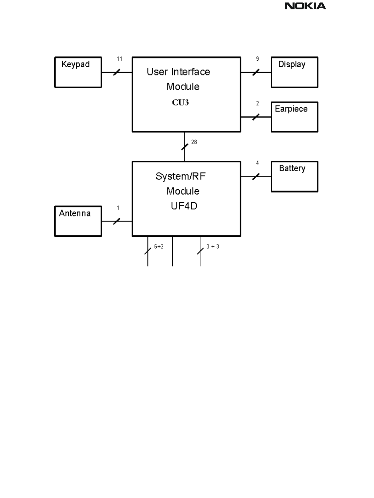
Transceiver NSD-6
Introduction
The NSD–3 is a tri–mode radio transceiver unit for the CDMA 800/1900MHz and AMPS
network. The transceiver is true 3 V transceiver. The transceiver consists of System/RF
module ( UF4D/UF4I ), User interface module ( CU3 ), and assembly parts.
The transceiver has full graphic display, and the user interface is based on two soft keys.
The transceiver has leakage tolerant earpiece.
The antenna is either fixed or extendable according to the phone type.
External antenna connection is provided by rear RF connector.
Modes of Operation
There are five different operation modes:
– power off mode
– idle mode
– active mode
– charge mode
– local mode
In the power off mode only the circuits needed for power up are supplied.
In the idle mode circuits are powered down and only sleep clock is running.
In the active mode all the circuits are supplied with power although some parts might be
in the idle state part of the time.
The charge mode is effective in parallel with all previous modes. The charge mode itself
consists of two different state: charge and maintenance mode.
The local mode is used for alignment and testing.
Issue 1 04/01 Nokia Mobile Phones Ltd. Page 5
Page 6
NSD-6
System Module PAMS Technical Documentation
Interconnection Diagram
Page 6 Nokia Mobile Phones Ltd. Issue 1 04/01
Page 7

NSD-6
PAMS Technical Documentation System Module
System Module
Circuit Description
The transceiver electronics consist of the Radio Module, RF + System blocks, the UI PCB,
the display module and audio components. The key pad and the display module are connected to the Radio Module with connectors. System blocks and RF blocks are interconnected with PCB wiring. The Transceiver is connected to accessories via a bottom system
connector with charging and accessory control.
The RF block is designed for a handportable phone which operates in the CDMA 800 system. The purpose of the RF block is to receive and de-modulate the radio frequency signal from the base station and to transmit a modulated RF signal to the base station.
Connectors
System Connector
B side view
Engine PCB
A side view
Fixing pads (2 pcs)
DC Jack
Charger pads (3 pcs)
1
Microphone
acoustic ports
8
7
14
Bottom
connector (6 pads)
Cavity for microphone
IBI connector
(6 pads)
Cable locking holes (3 pcs)
Note: Intelligent Battery Interface, IBI, is an accessory interface on the battery side of
the phone including the same signals as the bottom connector. The accessory ( e.g. an IBI
accessory) can be a battery pack with special features or an accessory module attached
between the phone and a normal battery pack.
Issue 1 04/01 Nokia Mobile Phones Ltd. Page 7
Page 8

NSD-6
System Module PAMS Technical Documentation
Pin Name Function Description
1 V_IN Bottom charger contacts Charging voltage
2 L_GND DC Jack Logic and charging ground
3 V_IN DC Jack Charging voltage
4 CHRG_CTRL DC Jack Charger control
5 CHRG_CTRL Bottom charger contacts Charger control
6 MICP Microphone Microphone signal; positive node
7 MICN Microphone Microphone signal; negative node
8 XMIC Bottom & IBI connectors Analog audio input
9 SGND Bottom & IBI connectors Audio signal ground
10 XEAR Bottom & IBI connectors Analog audio output
11 MBUS Bottom & IBI connectors Bidirectional serial bus
12 FBUS_RX Bottom & IBI connectors Serial data in
13 FBUS_TX Bottom & IBI connectors Serial data out
14 L_GND Bottom charger contacts Logic and charging ground
ÁÁÁ
RF Connector
The RF–connector is needed to utilize the external antenna with Car Cradle. The RF–connector is located on the back side of the transceiver on the top section. The connector is
plug type connector with special mechanical switching.
Accessory side of connector
Part will be floating in
car holder
Phone side of connector
Page 8 Nokia Mobile Phones Ltd. Issue 1 04/01
Page 9

NSD-6
PAMS Technical Documentation System Module
Baseband Module
Block Diagram
TX/RX SIGNALS
Cafe SUPPLY
RF SUPPLIES
PA SUPPL Y
SYSTEM CLOCK
19.2MHzCLK
UI
BASEBAND
Baseband Elements
Baseband refers to all technology elements in the phone design, which do not include RF
functions. The Baseband Module therefore includes audio, logic control, signal processing, power supply, and user interface functions. Baseband functionality of this product
consists of third generation Digital Core Technology (DCT3) design solutions.
Cafe
MEMORIES
AUDIOLINES
MAD
+
CCONT
BB SUPPLY
SYSCON
CHARGING
SWITCH
SLEEP CLOCK
32kHz
CLK
VBAT
BATTERY
Baseband ASICS Description
MAD4
The MAD4 ASIC contains four main components: DSP, MCU, RAM, and ROM. This ASIC
controls logic functions for the user interface, USART and PWMs, CAFÉ, Control Timing
and Interrupts (CTI), RX Modem, RF Interface, Accessory Interface, and CDMA functionality.
The DSP controls the RF power and implements the compressor and e-pander for AMPS,
the vocoders for CDMA and DTMF tone generation.
The MCU performs tasks such as UI control, timers, PUP control, RX Modem interface,
audio control, evaluation of sensor data from CCONT A\D, and battery charging control.
CAFÉ
The CAFÉ ASIC provides CODEC functionality (A/D and D/A conversions for voice data,
Issue 1 04/01 Nokia Mobile Phones Ltd. Page 9
Page 10

NSD-6
System Module PAMS Technical Documentation
microphone and speaker amplification, variable RX and TX Audio Gain), provides system
clock squaring, utilizes PLL for CDMA clock generation from system clock, and interfaces
to the RF section and to MAD4.
CCONT
The CCONT ASIC provides linear regulated power to most of the phone. It has a multiplexed A/D converter for temperature sensor digitization, battery voltage, charger voltage, current consumption, and battery type detection. An external 32 kHz oscillator
circuit is connected to CCONT, which is used for sleep clock generation. It also has a
watchdog circuit used to power off the phone in the event that MCU receives an interrupt from power key depression, or an event has caused a process to over run and MCU
does not service the register to prevent the watchdog timer from timing out.
PENTA
The PENTA IC chip operates as a low noise, low drop out regulator with 5 independent
2.8–volt outputs used to power on various sections of the RF module. The PENTA IC has 5
control inputs controlled by the MAD4 ASIC.
CHAPS
CHAPS operates as an integrated power switch for controlling charger current. Its features are limited start up current, limited maximum switch current, transient voltage
protection, voltage limit protection, and reverse voltage protection. It is designed to be
used with either a single lithium cell or three nickel cells battery types.
Memories
SRAM
External SRAM is used by MAD4. Size is 2 Mbit (256k x 8 bit).
FLASH MEMORY
Flash memory contains the main program code for the MCU and default EEPROM values.
Refer to the table below.
EEPROM
An EEPROM is used to store user data and tuning parameters. Refer to the table below.
FLASH Memory EEPROM Memory
NSD-6HX, 6GX 32 Mbit (2M x 16 bit) 1024kbit (128 x 8 bit)
Clocks
System Clock and CDMA Clock
A 19.2 MHz signal is passed to the CAFÉ ASIC from the RF section. The CAFÉ then generates the 19.2 MHz system clock and the 9.8304 MHz CDMA clock, which are derived
from the RF signal. Both of these clocks are passed to MAD4.
Page 10 Nokia Mobile Phones Ltd. Issue 1 04/01
Page 11

NSD-6
PAMS Technical Documentation System Module
8kHz Frame Sync Clock
An 8 kHz frame sync is generated in MAD4 and passed to the CAFÉ in order to synchronize the internal CAFÉ clocks with the equivalent MAD4 clocks. This signal is also used to
“frame” the CODEC voice data at 8kHz. The pulse width of the frame sync will be equal to
one period of the 320 kHz clock, which is internal to CAFÉ.
Sleep Clock
Sleep clock is provided by CCONT and produces a 32.768 kHz clock used by MAD4 when
it is in sleep mode. The crystal oscillator in the external CCONT circuitry to CCONT is not
automatically started when the battery is connected, but after power up the oscillator is
always running, even during power off periods. The only exception is when the battery is
removed.
UIF and CCONT Serial Clock (UIF_CCONT_SCLK)
This 960 KHz clock is used to synchronize serial data transmission on the UIF and CCONT
serial data bus UIF_CCONT_SDIO.
Issue 1 04/01 Nokia Mobile Phones Ltd. Page 11
Page 12

NSD-6
System Module PAMS Technical Documentation
Baseband Power Distribution
Description
Power management and distribution in the phone is handled by the CCONT asic. CCONT
is a multi function power management IC which has seven 2.8V linear regulators for the
RF–section of the phone. One 2.8V regulator is used to power up the baseband of the
phone, and its output is called Vbb. Additionally, one adjustable regulator is used to power up certain parts of the baseband. There are also a 5V charge pump, 5V regulator and a
3/5V regulator.
The main functions are voltage regulation, power up/down procedures, reset logic,
charging control (PWM) , watchdog, sleep control, ADC and real time clock.
CCONT Regulators
Battery voltage VBAT is connected to CCONT which regulates all the supply voltages VBB,
VR1–VR7, V2V, VR1_SW, VSIM and V5V. CCONT’s default startup mode is to turn on VR1,
VBB, V2V, VR6 and Vref in power–up. Vrefs default value is 1.5V, but in in this phone we
use 1.25V for Vref, so one of the first things MAD4 does on power up is to do a write to
Page 12 Nokia Mobile Phones Ltd. Issue 1 04/01
Page 13

NSD-6
PAMS Technical Documentation System Module
CCONT to change Vref to 1.25V.
VBB is used as baseband power supply for all digital parts, and it is on whenever the
phone is powered up. V2V is reserved for a later version of the MAD4 ASIC which will
have a lower core voltage. When the low voltage core version of MAD4 is available, V2V
will be connected to those pins on MAD4 which power the core. VSIM is used as programming voltage for the Flash memory after the phone is cut out of the panel. This is
necessary if re–flashing is needed after initial flash programming in production. V5V is
used for RF parts only. VR6 supplies the power for CAFE.
VR1 is used for the VCTCXO supply. VR1_SW is derived from VR1 inside CCONT, and is
actually the same voltage, but can be separately switched on and off. This VR1_SW is
used as an optional external microphone bias voltage. CLK_EN signal to CCONT controls
both the VR1 and VR6 regulators; they can be switched off in sleep modes, during
standby.
CCONT regulators are controlled through a seial data bus from MAD4. Regulators VR3, 4,
5 and 7 are controllable through external pins; these pins forming a logical ’OR’ function
with the serial commands. If a regulator’s control pin is at logic ’1’, that regulator will
turn on. If the pins are not used for external control they are grounded.
Most of the regulator outputs depend on pin control. In the table the ’State in reset’ is
based on assumption that pin controls are ’0’.
Charging
Charging can be performed in any operating mode. The charging algorithm is dependent
on the battery technology used. A resistor internal to the battery pack indicates the battery type. The resistor value corresponds to a specific battery capacity. This capacity
value is related to the battery technology as different capacity values are achieved by
using different battery technologies.
The CCONTs A/D converter input measures the battery voltage, temperature, size and
current.
NOTE: Power management circuitry controls the charging current delivered from the
charger to the battery. Charging is controlled with a PWM input signal from CCONT. The
pulse width is controlled by MAD4 and is sent to CCONT through a serial bus. The battery
voltage rise is limited by turning CHAPS switch off when the battery voltage has reached
the desired limits.
Watchdog
MAD4 must reset the CCONT watchdog regularly. CCONT watchdog time can be set
through SIO between 0 and 63 seconds at 1 second steps. After power–up the default
value is 32 seconds. If the watchdog expires, CCONT will cut off all supply voltages. After
total cut–off the phone can be re–started through any normal power–up procedure.
CCONTs watchdog functionality may be temporarily disabled by holding CCONTs
PWRONX/WDDISX pin at logic low.
Issue 1 04/01 Nokia Mobile Phones Ltd. Page 13
Page 14

NSD-6
System Module PAMS Technical Documentation
Power Up
There are four ways to power on the phone.
1. Pressing the power button
2. Connecting a charger
3. An IBI interrupt on BTEMP
4. Internal RTC times out.
Each of four methods is described in general in the following sections. When the battery
is connected to phone, nothing will happen until the power–up procedure is initiated, for
instance by pressing the power–button or by connecting a charger. After that the 32kHz
crystal oscillator of CCONT is started (can take up to 1 sec), and the default regulators
are powered up.
If a power down is done and the battery remains connected, the 32 kHz crystal oscillator
keeps running in the CCONT.
VCTCXO
CAFE
FLASH
RF
VR1–VR7
VCHAR
CHAPS
VBAT
PWM
BATTERY
CCONT
VR1_SW
MAD
VR1
VR6
VBB
SIO
VSIM
V5V
Vref
Power distribution diagram
Page 14 Nokia Mobile Phones Ltd. Issue 1 04/01
Page 15

NSD-6
PAMS Technical Documentation System Module
Pressing power key
PWRONX
VR1, VBB, VR6
CLK_EN
VCTCXO
CAFE CLK
PURX
SLCLK
t1
t2
t3
t1 < 1 ms
t2 1 - 6 ms, VCXO settled
t3 62 ms, PURX delay generated by CCONT
After PWR–key has been pushed, CCONT gives PURX reset to MAD4 and turns on VR1,
VBB and VR6 regulators (if battery voltage has exceeded 3.0 V). VR1 supplies VCTCXO,
VBB supplies MAD, and VR6 supplies digital parts of CAFE. After the initial delay, t2,
VCTCXO starts to give a proper 19.2MHz clock to CAFE, which further divides it to
9.83MHz for MAD4. CAFE will output the 9.83MHz clock only after the PURX reset has
been removed. After delay, t3, CCONT releases PURX and MAD4 can take control of the
operation of the phone.
After MAD4s reset is released MCU–SW detects that the PWR–key is still pushed and
shows the user that the phone is powering up by turning on the LCD and the lights.
MCU–SW then powers up the RF receiver part.
V5V–regulator (for RF) default value is off in power–up, and can be con-trolled on via
serial bus when needed.
Issue 1 04/01 Nokia Mobile Phones Ltd. Page 15
Page 16

NSD-6
System Module PAMS Technical Documentation
Power up when charger connected
Normal battery voltage
VCHAR
VR1, VBB, VR6
CLK_EN
VCTCXO
9.83 MHz CLK
PURX
SLCLK
CCONTINT
t1
t2
t3
Power up, charger connected, VBAT > 3.0 V
Power up, charger connected, VBAT > 3.0 V
The power up procedure is similar to the process described in the previous chapter with
the exception that the rising edge of VCHAR triggers the power up in CCONT.
CCONT sets output CCONT_INT, MAD4 detects the interrupt and reads CCONT status register to find the reason for the interrupt (charger in this case). After reading the A/D register to determine that the charger voltage is correct MAD should initiate charging
activities. The phone will remain in the so called ”acting dead” state which means that
only the battery bars are displayed on the LCD. The user perceives that the phone is off. If
the power on button is pushed the LCD display will come on and startup will be the same
as normal power on.
CCONT_INT is generated both when the charger is connected, and when the charger is
disconnected.
Page 16 Nokia Mobile Phones Ltd. Issue 1 04/01
Page 17

NSD-6
PAMS Technical Documentation System Module
Empty battery
VBAT > 3.0 V
VCHAR
VR1, VBB, VR6
CLK_EN
VCTCXO
9.83MHz
PURX
SLCLK
CCONT_INT
Power up, charger connected, VBAT < 3.0 V
Before battery voltage voltage rises over 3.0 V CHAPS gives an initial charge (with limited current) to the battery. After battery voltage reaches 3.0V the power up procedure is
as described in the previous section.
If a power down is done and the battery remains connected, the 32 kHz crystal oscillator
keeps running in the CCONT. When a power–up is initiated again, the complete power–
up sequence is described in the figure below. This time the power–up sequence is faster
because the oscillator is already running.
Charging – CHAPS
CHAPS comprises the hardware for charging the battery and protecting the phone from
over–voltage in charger connector.
The main functions are:
t1
t2
t3
–transient, over–voltage and reverse charger voltage protection
–limited start–up charge current for a totally empty battery
–voltage limit when battery removed
–with SW protection protection against too high charging current
CHAPS is basically a PWM (Pulse Width Modulation) controlled switch which connects
Issue 1 04/01 Nokia Mobile Phones Ltd. Page 17
Page 18

NSD-6
System Module PAMS Technical Documentation
the charger to VBAT. MAD4 controlls CHAPS by writing PWM values to CCONTs PWM
register over a serial bus. CCONT thenoutputs a PWM which is used by CHAPS to control
the switch. In the case of an external fast charger, the PWM is available at the system
connector to control the charger. In the case of a dead battery, shorted battery, or if the
battery is below 3.0V, CHAPS supplies a controlled leakage current of about 180mA
through the switch to attempt to bring the battery voltage up.
Pin
Number
1, 16 VCH Charger voltage input
5 RSENSE High current output, connected to current sense resistor of phone
12 VBAT Battery voltage (connected to voltage sense part of CHAPS)
10 VBACK Backup battery charging voltage output
9 LIM Output voltage limit select input
7 PWM Charging switch control input
8 CTIM External capacitor for soft switching
2,3,4,6,11
13,14,15
Name Description
GND Ground
CHAPS
Vin
BATTERY
MAD
System
Connector
To
charger
PWMOUT
Charging Control
CCONT
serial control
V_charge
2–wire charging
With 2–wire charging the charger provides constant output current, and the charging is
controlled by PWMOUT signal from CCONT to CHAPS. PWMOUT signal frequency is
selected to be 1 Hz, and the charging switch in CHAPS is pulsed on and off at this frequency. The final charging current to the battery is controlled by adjusting the PWMOUT
signal pulse width.
Both the PWMOUT frequency selection and pulse width control are made by the MCU
which writes these values to CCONT.
Page 18 Nokia Mobile Phones Ltd. Issue 1 04/01
Page 19

NSD-6
PAMS Technical Documentation System Module
The 2–wire charger is part number ACP–7, has full–wave rectified output, defined output
voltage and impedance. Typical output current into empty battery is about 350 mA at
nominal mains voltage.
3–wire charging
With 3–wire charging the charger provides adjustable output current, and the charging
is controlled by PWMOUT signal from CCONT to Charger, with the bottom connector signal. PWMOUT signal frequency is selected to be 32 Hz, and the charger output voltage is
controlled by adjusting the PWMOUT signal pulse width. The charger switch in CHAPS is
constantly on in this case.
The 3–wire charger is part number ACP–9, a switch mode power supply (SMPS) adapter
using 3–wire charging structure (controlled constant voltage). Typical output into an
empty battery is about 850mA at nominal mains voltage.
Battery disconnected when charger is connected
From hardware point of view the phone could otherwise continue functioning normally,
but if the charger voltage is higher than the maximum allowed battery voltage, this can
damage the RF parts. Therefore, output overvoltage protection is needed in case the battery is removed when a charger is connected, or if a charger is connected before the battery to the phone. With a charger connected, if VBAT exceeds preset limits in CHAPS, the
switch turns OFF immediately (soft switching bypassed). There are two voltage limits,
VLIM1 and VLIM2. VLIM input = ’0’ selects VLIM1, VLIM input = ’1’ selects VLIM2.
Parameter Symbol Min Typ Max Unit
Output voltage cutoff limit (during
transmission or Li-battery)
Output voltage cutoff limit (no
transmission or Ni-battery)
VLIM1 4.4 4.6 4.8 V
VLIM2 4.8 5.0 5.2 V
When the switch turns off due to an overvoltage condition, it stays off until the input
voltage falls below the specified limit (VCH<VBAT). Phone software will stop the charging as fast as it detects that there is no battery present.
Issue 1 04/01 Nokia Mobile Phones Ltd. Page 19
Page 20

NSD-6
System Module PAMS Technical Documentation
VBAT
VLIM
4V
t
PWM
”1”
”0”
t
WITCH
1. Battery removed, (standard) charger connected, VBAT rises (follows charger voltage).
2. VBAT exceeds limit VLIM(X), switch is turned immediately OFF.
3. VBAT falls (no battery), also VCH<VBAT (standard chargers full-rectified output). When
VCH>VBAT and VBAT<VLIM(X) -> switch turned on again (also PWM is still HIGH) and
VBAT exceeds VLIM(X).
4. Software sets PWM = LOW -> CHAPS does not enter PWM mode.
Output overvoltage protection when battery removed (in principle).
Power Down
Pressing power key
ON
OFF
21 3 4
t
When the user wishes to turn the phone off and presses the power key, MAD (MCU SW)
detects that PWR–key is pressed for a long enough time. After that the lights and LCD
are turned off. MCU stops all the activities it was doing (e.g. ends a call), sends power off
command to CCONT by writing a ’zero’ amount of time to the watchdog register, and
goes to idle–task. After the delay CCONT cuts all the supply voltages from the phone.
Only the 32 kHz sleep clock remains running.
Note that the phone doesn’t go to power off (from HW point of view) when the charger
is connected and PWR–key is pushed. The user perceives that the phone is off, but in fact
Page 20 Nokia Mobile Phones Ltd. Issue 1 04/01
Page 21

NSD-6
PAMS Technical Documentation System Module
the phone is just acting as if it is off (this state is usually called ”acting dead”).
Battery charge low
As a battery discharges, energy management software keeps a constant watch on the
voltage and displays an appropriate amount of battery bars.
When the battery discharges to a critical level the software notifies the user by beeping.
If left on, the software will power off the phone at a VBAT of TBD V.
If the SW fails to power down the phone, hardware will take over and CCONT will do a
reset and power down the phone when the battery voltage drops below 2.8 V.
Watchdog expires
If the SW fails to update the watchdog, the watchdog will eventually expire and CCONT
cuts all the supply voltages to the phone. On startup, the initial value set in CCONT’s
watchdog timer register is 32.5 seconds. The watchdog is programmable from 0 to 63
seconds.
Disconnected battery
When battery is disconnected, immediate and totally uncontrolled power–down happens. Therefore a power off procedure in this case cannot be described. One possible risk
is that if the MCU is writing something to the EEPROM exactly at the same moment, the
memory contents may be corrupted.
RF to Baseband Interface
The RF to Baseband interface consists of MAD4 and CAFÉ communicating with various
parts of the RF module. The MAD4 ASIC produces the Pulse Duration Modulators (PDMs)
which allow analog voltages to be used for RF control. It also controls the VCTCXO
enable, as well as band and mode selects. MAD also controls the RF supply voltages
through CCONT. The CAFÉ ASIC performs the A/D and D/A conversions for CDMA and
AMPS RX and TX paths. CAFÉ also receives the VCTCXO 19.2 MHz signal and provides
MAD4 with the 19.2 MHz system clock.
Audio control
Audio Controls and Processing
The audio control is handled by the MAD4 MCU. Speech coding functions are performed
in MAD4 DSP. In transmission mode, the speech code is sent to CAFÉ ASIC for D/
A conversion. In receiver mode, PCM coded blocks are read from the CAFE ASIC Both
audio and RF CODECs reside in CAFÉ.
Earpiece
The internal earpiece is connected to the UI board by means of mounting springs for
Issue 1 04/01 Nokia Mobile Phones Ltd. Page 21
Page 22

NSD-6
System Module PAMS Technical Documentation
automated assembly. The 32–ohm impedance, dynamic type earpiece is connected to the
differential output of the CAFÉ ASIC.
Microphone
The internal microphone is connected to the bottom connector by means of mounting
springs. The microphone bias is provided by the CAFÉ ASIC.
Audio Accessory Interface
External audio is interfaced to the phone through the system connector. XEAR, XMIC,
and SGND are the phone’s external audio signal pins used for communication during a
hands free accessory call.
Digital control
MAD4
The baseband functions are controlled by the MAD asic, which consists of a MCU, a system ASIC and a DSP. The CDMA specific asic is named as MAD4.
MCU
For general purpose processing applications.
DSP
The DSP is in charge of the channel and speech coding. The Main interfaces are to the
MCU, and via System Logic to CAFE and RF.
System Logic
Peripheral interface:
_ MCU Parallel I/O, UART, and PWM control (PUP)
Serial Accessory Interface (FBUS):
_ Autobauding support (AccIf)
_ Interface to external memories
_ Address lines and chip select decoding (BUSC)
_ RF Interface and Control (RFIfCtrl)
_ Clocking, timing and interrupts (CTI)
_ Sleep Control (SleepBlk)
_ CAFE Control (CAFECtrl)
Page 22 Nokia Mobile Phones Ltd. Issue 1 04/01
Page 23
NSD-6
PAMS Technical Documentation System Module
User Interface Control (UserIf)
Reset Generator (RstGen)
Clock Generator (ClkGen)
Test Interface (TestIf)
MAD Interfaces
UI and CCONT Serial interface
MAD4s serial interface is used to control the Serial LCD on the User Interface board, and
to provide access to CCONTs registers. The DataSelX and DataClk are generated by MAD4
during both transmit and receive cycles. Each device has its own chip select signal and
must hold its data pin in a high impedance state if its chip select is not active. Data must
be valid on the rising edge of DataClk during both transmit and receive.
CAFE Interface
The MAD4 ASIC supplies an interface to the CAFE ASIC. This interface consists of parallel
transmit and receive busses for CDMA and AMPS data, and a serial interface for Codec
control and data.
FBUS
FBUS (Fast Bus) is a fast serial interface between the DSP and data accessories or the
DSP and multipath analyzer. This interface is a full–duplex, asynchronous, two–line bus.
Tsds
Tsdh
mdMCUSDIO (Serial Clk)
accFBusRXD (Serial Data)
Data 0 Data 1
...
Data 7
USART Synchronous Mode Receive (Flashing Mode)
MBUS
MBUS is the MCUs serial interface which is used for FLASH downloading (not program
code), testing, and communication with external devices. Supported baud rates are 9.6,
19.2, 38.4 and 57.6 kbit/s.
JTAG Interface
The JTAG interface is used for MAD4 ASIC emulation. This interface provides for coemulation of the DSP and MCU.
Issue 1 04/01 Nokia Mobile Phones Ltd. Page 23
Page 24

NSD-6
System Module PAMS Technical Documentation
TRUST Interface
TRUST (Trace Utility for Software Testing) is a hardware module used to capture tracing
data from a phone during testing. It serves as a buffer memory, storing data from the
address and data buses of the phone MCU until read by a PC. A time label is attached to
each data word. The unit also includes a buffer for commands from the PC to the phone.
Page 24 Nokia Mobile Phones Ltd. Issue 1 04/01
Page 25

NSD-6
PAMS Technical Documentation System Module
Signal Definitions
SIGNAL NAME DESCRIPTION From/To
Busses, Strobes, and Clocks
Includes parallel and serial busses as well as data clocks and chip selects
ADD(20:0) 21-bit Memory Address Bus MAD4 to FLASH and
SRAM
DATA(15:0) 16-bit Memory Data Bus MAD4 to FLASH and
SRAM
RXD(11:0) Receive Data CAFE to MAD4 0 to 2.8V Digital
TXD(7:0) Transmit Data MAD4 to CAFE 0 to 2.8V Digital
EEPROMSCLK SCLK to serial EEPROM MAD4 to EEPROM 0 to 2.8V Digital
EEPROMSDA Serial data line for serial EEP-
ROM
UIF_CCONT_SCLK Clock for UI and CCONT serial
interface
UIF_CCONT_SDIO User interface and CCONT
Serial Data
CCONTCSX CCONT Chip Select MAD4 to CCONT 0 to 2.8V Digital
MAD4 to EEPROM 0 to 2.8V Digital
MAD4 to CCONT and
UI connector
MAD4 to CCONT and
UI connector
Signal
Characteristics
0 to 2.8V Digital
0 to 2.8V Digital
(Pullup)
0 to 2.8V Digital
0 to 2.8V Digital
Notes
LCDCS LCD Chip Select MAD4 to UI connector 0 to 2.8V Digital
MEM(3) Memory Read Strobe MAD4 to FLASH and
SRAM
MEM(2) Memory Write Strobe MAD4 to FLASH and
SRAM
MEM(1) RAM Chip Select MAD4 to SRAM 0 to 2.8V Digital
MEM(0) FLASH chip enable MAD4 to FLASH 0 to 2.8V Digital
MBUS MCU serial bus for external
communication
FBUS_TX DSP accessory UART Data
Output
FBUS_RX DSP accessory UART Data
Input
ADATA AMPS Data Input to Rx
Modem (MAD4)
CAFESIO(2) CAFE I/F Frame Sync MAD4 to CAFE 0 to 2.8V Digital
CAFESIO(1) CAFE I/F Serial Data from
CAFE
MAD4 to system connector
MAD4 to system connector
System connector to
MAD4
CAFE to MAD4 0 to 2.8V Digital
CAFE to MAD4 0 to 2.8V Digital
0 to 2.8V Digital
0 to 2.8V Digital
0 to 2.8V Digital
0 to 2.8V Digital
0 to 2.8V Digital
CAFESIO(0) CAFE I/F Serial Data to CAFE MAD4 to CAFE 0 to 2.8V Digital
Issue 1 04/01 Nokia Mobile Phones Ltd. Page 25
Page 26

NSD-6
System Module PAMS Technical Documentation
SIGNAL NAME DESCRIPTION From/To
Busses, Strobes, and Clocks
Includes parallel and serial busses as well as data clocks and chip selects
CLK9M20 19.2MHz System Clock CAFE to MAD4 0 to 2.8V Digital
CLK9M83 9.8304MHz CDMA Clock CAFE to MAD4 0 to 2.8V Digital
SLEEPCLK 32.768kHz Sleep Clock CCONT to MAD4 0 to 2.8V Digital Osc. run-
RF Interface Control Signals
CAFE_TX_GATE Transmitter Gating Signal MAD4 to RF 0 to 2.8V Digital
TIF_EN TIF chip enable MAD4 to RF 0 to 2.8V Digital
SYN_ACQ&SYN_
PWR_DN
SYN_LK1 MAD4 to RF 0 to 2.8V Digital
RIF_EN MAD4 to RF 0 to 2.8V Digital
MAD4 to RF 0 to 2.8V Digital
Signal
Characteristics
Notes
ning while
phone is
powered
down.
TX_LIM Indicates TX Power Greater
than TXI_REF
SYN_CLK R/F I/F Serial Clock MAD4 to RF 0 to 2.8V Digital
SYN_DAT R/F I/F Serial Data MAD4 to RF 0 to 2.8V Digital
SYN_LE1 R/F I/F Serial Latch Enable #1 MAD4 to RF 0 to 2.8V Digital
CEL_MODE R/F I/F Serial Latch Enable #2 MAD4 to RF 0 to 2.8V Digital
BAND_SEL RF Frequency Band Select
(PCS or Cellular)
MODE_SEL RF Mode Select (CDMA or
AMPS)
AFC AFC PDM MAD4 to RF 0 to 2.8V conti-
RX_IF_AGC Receive IF AGC PDM MAD4 to RF 0 to 2.8V conti-
TX_IF_AGC Transmit IF AGC PDM MAD4 to RF 0 to 2.8V conti-
TX_RF_AGC Transmit RF AGC PDM MAD4 to RF 0 to 2.8V conti-
RF to MAD4
MAD4 to RF 0 to 2.8V Digital
MAD4 to RF 0 to 2.8V Digital
nously variable
nously variable
nously variable
nously variable
TX_VCO_CAL PENTA Regulator control (PS) MAD4 to RF 0 to 2.8V Not used
as a PDM
TX_LIM_ADJ General Purpose PDM2 MAD4 to RF 0 to 2.8V continu-
ously variable
Page 26 Nokia Mobile Phones Ltd. Issue 1 04/01
Page 27

NSD-6
PAMS Technical Documentation System Module
SIGNAL NAME DESCRIPTION From/To
RF Interface Control Signals
FILT_SEL General Purpose PDM3 MAD4 to RF 0 to 2.8V Digital Not used
BOOST General Purpose PDM4 MAD4 to RF 0 to 2.8V conti-
RX_GS MAD4 to RF 0 to 2.8V Digita
RF_TX_GATE_P MAD4 to RF 0 to 2.8V Digita
RF_TX_GATE_C MAD4 to RF 0 to 2.8V Digita
CLK_EN MAD4 to CCONT 0 to 2.8V Digita Signal to
VLIM Used to select the max bat-
tery voltage for the charging
circuit in CHAPS (VLIM1 or
VLIM2)
MAD4 to CHAPS 0 to 2.8V Digital
Signal
Characteristics
nously variable
Notes
as a PDM
CCONT
which controls regulators to RF
Peripherals, Accessory Interface, and A/Ds
BUZZER Buzzer PWM Output MAD4 to UI connector 0 to 2.8V Digital
VIBRA PWM output for vibra motor MAD4 to on board
VIBRA circuit, and to
battery connector via
BTEMP line
HOOKINT Hook Interrupt CAFE to MAD4 0 to 2.8V Digital
EAD_HEADINT Headset Interrupt (CCONT
performs A/D on this signal)
tp4 DBUS data line test point MAD4 0 to 2.8V Digital
RS232_PWR Control for switching power
onto SGND while using a
data cable accessory
BSI Intelligent Battery Interface.
A/D input to CCONT
BTEMP A/D input to CCONT. Used for
battery temperature detection and battery VIBRA control
CAFE to MAD4 and
CCONT
N306 (regulator) to
system connector
Battery connector to
CCONT
Battery Connector to
CCONT
0 to 2.8V Digital
0 to 2.8V Digital
0 to 2.8V Digital Controlled
DC voltage level
that varies with
different battery
types
DC voltage level
which changes
with battery temperature
by MAD4
Voltage
divider A/D
input to
CCONT
Thermistor
voltage
divider A/D
input to
CCONT
Issue 1 04/01 Nokia Mobile Phones Ltd. Page 27
Page 28

NSD-6
System Module PAMS Technical Documentation
SIGNAL NAME DESCRIPTION From/To
Peripherals, Accessory Interface, and A/Ds
PA_TEMP A/D input to CCONT. Used for
RF power amp temperature
detection.
RSSI A/D input to CCONT. Receive
signal strength indicator for
AMPS mode
V_IN Power in from charger System connector to
L_GND Ground reference for charger
(Separated from GND
through an inductor)
RF to CCONT DC voltage level
RF to CCONT DC voltage level
CHAPS
System connector to
GND via inductor
Signal
Characteristics
which changes
with PA temperature
which changes
with received signal strength
ACP-9 DC
ACP-7 Rectified
AC
0V
Notes
Thermistor
voltage
divider A/D
input to
CCONT
Voltage
will change
with
charge
control
PWM
Regulator Control Signals
VREGP1 Controls voltage regulator P1
(PENTA)
VREGP2 Used to control voltage regu-
lator P2 (PENTA). This signal
is also the MSB (bit-21) of
the Memory Address Bus but
is not used as an address bit
VREGP3 Controls voltage regulator P3
(PENTA)
VREGP4 Controls voltage regulator P4
(PENTA)
CCONT_INT CCONT interrupt to MAD4 CCONT to MAD4 0 to 2.8V Digital
User Interface Board Peripherals
FLIP Flip interrupt (detects status
of hinge) on variants with flip
feature
BACKLIGHT Controls illumination on UI
board
MAD4 to CCONT 0 to 2.8V Digital
MAD4 to CCONT 0 to 2.8V Digital
MAD4 to CCONT 0 to 2.8V Digital
MAD4 to CCONT 0 to 2.8V Digital
UI connector to MAD4 0 to 2.8V Digital
MAD4 to UI connector 0 to 2.8V Digital
CALL_LED Controls the call LED on UI
board
MAD4 to UI connector 0 to 2.8V Digital
Page 28 Nokia Mobile Phones Ltd. Issue 1 04/01
Page 29

NSD-6
PAMS Technical Documentation System Module
SIGNAL NAME DESCRIPTION From/To
User Interface Board Peripherals
LCD_RESETX Resets the LCD on the UI
board
COL(4:0) Keyboard columns on UI
board
UIF(5:0) Keyboard rows and LCD I/F MAD4 to UI connector 0 to 2.8V Digital
PWRONX Power button signal UI connector to MAD4 0 to 2.8V Digital
Resets
PURX Power Up Reset CCONT to MAD4 0 to 2.8V Digital
RESETX System Reset MAD4 to CAFE 0 to 2.8V Digital
CAFE RF/IF
IQSEL IQ Select control line for
selecting I or Q data
RXIQ(3:0) CDMA Receive I and Q data RF to CAFE Differential I and
MAD4 to UI connector 0 to 2.8V Digital
MAD4 to UI connector 0 to 2.8V Digital
MAD4 to CAFE 0 to 2.8V Digital
Signal
Characteristics
Differential Q
Notes
TXIQ(3:0) CDMA Transmit I and Q data CAFE to RF Differential I and
Differential Q
LIM_P non-inverting AMPS receive
modulated signal
LIM_N inverting AMPS receive mod-
ulated signal
CLK19M2RF 19.2MHz sinusiod from RF RF to CAFE sinusoid
AMPSMOD AMPS audio signal (after DSP
and D/A) to be transmitted
Test & Emulation
JTAG_TRST JTAG Reset MAD4 0 to 2.8V Digital
JTAG2_TDI JTAG Scan Input MAD4 0 to 2.8V Digital
JTAG3_TDO JTAG Scan Output MAD4 0 to 2.8V Digital
JTAG4_TCK JTAG Clock & ATPG Scan
Clock
JTAG5_PD JTAG Mode Select & ATPG
Scan Enable
RF to CAFE analog
RF to CAFE analog
CAFE to RF analog (voice)
MAD4 0 to 2.8V Digital
MAD4 0 to 2.8V Digital
JTAG0 DSP/MCU Emulation (NOT
USED)
JTAG6 DSP/MCU Emulation (NOT
USED)
MAD4 0 to 2.8V Digital
MAD4 0 to 2.8V Digital
Issue 1 04/01 Nokia Mobile Phones Ltd. Page 29
Page 30

NSD-6
System Module PAMS Technical Documentation
SIGNAL NAME DESCRIPTION From/To
Test & Emulation
DSP External Flag (NOTE: This
pin has a dual function as
General Purpose I/O
“P0GPIO(6)”. DSPXF is default
function.)
CHRG_CTRL_A DSP Serial Port Input Clock
(for multipath analyzer)
TP5 DSP Serial Port Frame Sync
(for multipath analyzer)
WDDI Watchdog disable Test connector to
CCONT Outputs
VBB LEAD power pins (DSP) CCONT to MAD4 and
MAD4 0 to 2.8V Digital
MAD4 0 to 2.8V Digital
MAD4 0 to 2.8V Digital
CCONT
memories as the UI
connector
Signal
Characteristics
0 to 2.8V Digital Used in
2.8V regulator
Notes
factory
while still
in panel
VR1_SW Power for microphone bias CCONT to V201
(CAFE)
VR1 Provides RF power to RF 2.8V regulator
VR2 Provides RF power to RF 2.8V regulator
VR3 Provides RF power to RF 2.8V regulator
VR4 Provides RF power to RF 2.8V regulator
VR5 Provides RF power to RF 2.8V regulator
VR6 Provides power to CAFE to RF 2.8V regulator
VR7 Provides RF power to RF 2.8V regulator
VR7A Provides RF power to RF 2.8V regulator regulator
VREF Used by CAFE as an A/D volt-
age reference
VMAD Provides power to the MAD4
core. Will be used only with
the ROM3 version of MAD4.
to CAFE 1.244V reference
CCONT to MAD4 1.8V regulator Program-
2.8V regulator
external to
CCONT
mable to
different
voltages
+5V_POWER Provides 5V power to RF to RF 4.7 to 5.2V Charge
pump
3V_5V Provides 3V to flash (Vpp) for
programming
CCONT to FLASH 2.7 to 3.3V Used at 3V
Page 30 Nokia Mobile Phones Ltd. Issue 1 04/01
Page 31

NSD-6
PAMS Technical Documentation System Module
SIGNAL NAME DESCRIPTION From/To
CCONT Outputs
CHRG_CTRL Charge control PWM signal
for accessories
Audio Signals
EARN Inverting part of the audio
differential signal to the earpiece
EARP Non-inverting part of the
audio differential signal to
the earpiece
System connector to
CHAPS. Can also be
driven by CCONT.
CAFE to UI connector 1.8Vp-p max Combined
CAFE to UI connector 1.8Vp-p max Combined
Signal
Characteristics
0 to 2.8V Digital
Notes
differential output
from earn
and earp is
3.6Vp-p
max
differential output
from earn
and earp is
3.6Vp-p
max
XEAR Single-ended audio signal to
bottom connector
CAFE Submodule
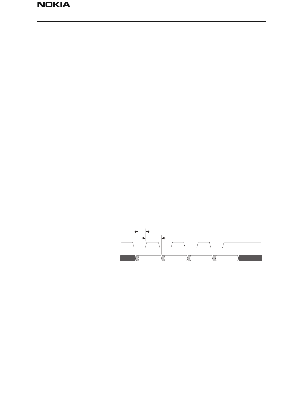
CDMA RX
The MAD/CAFE RX Interface consists of a 12–bit data bus RXD(11:0) output from the
CAFE ASIC to the MAD ASIC. In CDMA mode the data transfer rate is 9.8304MHz. The RX
data is clocked out of the CAFE ASIC on the falling edge of the 9.8304MHz clock, and
clocked into the MAD ASIC on the rising edge. For CDMA mode the 4–bit RXI data is supplied on bits RXD(5:2) and the 4–bit RXQ data is supplied on bits RXD(11:8). Bits (7), (6),
(1) and (0) are not used in CDMA mode.
CLK9M8O
RXD(11:0)
LAST VALUE READ DATA FROM CAFE LAST VALUE
Digital Mode RX Data Bus Timing
CAFE to system connector
t
DRXD
1.8Vp-p max Single
ended
t
DRXD
Issue 1 04/01 Nokia Mobile Phones Ltd. Page 31
Page 32

NSD-6
System Module PAMS Technical Documentation
CDMA TX
TXGATE
TXD(7:0)
CLK9M8O
IQSEL
DON’T
CARE
t
TXGS
t
TXGON
VALID DATA
FROM MAD
t
DSU
t
IQSU
IQ
VALID DATA
FROM MAD
t
DH
VALID DATA
FROM MAD
t
IQH
t
TXGOFF
DATA FROM
MAD
DON’T
CARE
t
TXGH
Digital Mode TX Data Bus Timing
AMPS RX
AMPS receive data from the RF section is differential, through pin 23 and 24 of the CAFE
ASIC. RX data is transferred at 40 kHz through a 12–bit data bus RXD(11:0) output from
the CAFE ASIC to the MAD4 ASIC. Wide band data (ADATA) is one bit asynchronous data
running at 150 kHz.
Data conversion and the bus interface is synchronous. Data is clocked out of CAFE on the
falling edge of the clock and clocked into the MAD4 on the rising edge of the clock.
AMPS TX
The TX data in AMPS mode is transferred at 120 kHz using an 8–bit multiplexed parallel
data bus TXD(7:0). The AMPS transmit channel uses the Q channel. TX data is clocked out
of MAD4 on the rising edge and clocked into the CAFE on the falling edge.
Page 32 Nokia Mobile Phones Ltd. Issue 1 04/01
Page 33

NSD-6
PAMS Technical Documentation System Module
System Connector
XEAR
RF Section
TXIQ(3..0)
CLK19M2
AMPS_MOD
LIM_N
LIM_P
RXIQ(3..0)
SGND
XMIC
MICP
MICN
CLK_EN
IQSEL
TXD(7..0)
MAD Module
RXD(7..0)
CAFE_TX_GATE
ADATA
CLK9M83
CLK19M20
RESETX
INTERUPTIONS
CAFE Module
CAFE and Peripherals Block Diagram
VREF
VR6
CCONT
Audio CODEC
The audio CODEC has the following functional blocks:
– 8 kHz interface for speech codec
– Microphone amplifiers and mux for three differential microphone inputs
– Variable gain amplifier for TX audio
– Variable gain amplifier for sidetone audio
– 13-bit Analog-to-Digital converter and lowpass filter
Issue 1 04/01 Nokia Mobile Phones Ltd. Page 33
Page 34

NSD-6
System Module PAMS Technical Documentation
– 13-bit Digital-to-Analog converter and lowpass filter
– Variable gain amplifier for RX audio
– Speaker amplifiers for three speakers
Transmit
The microphone signal, MICP and MICN, is sent to CAFE differentially through pin 66 and
pin 69. The maximum input signal level at either input is 1.0 V, which gives a differential
level of 2.0 V
pp
. Audio data is transferred in 16 bit frames (2 LSBs are not used).
The audio signal from an external accessory (XMIC) drives pin 68. The ground reference
for XMIC is SGND (pin 67), which is a virtual ground.
Receive
The audio receive path consists of a D/A converter, lowpass filter and output attenuator
with three selectable outputs. Only one output can be active at a time. The biasing at the
outputs can be independently controlled to be ON at all outputs to avoid switching transients.
The EAR output from pin 77 and pin 80 is intended to drive a phone earpiece having typically 32 ohm resistance. The output is differential, having positive (EARP) and negative
(EARN) output terminals.
The HF output is intended to drive external audio circuitry via XEAR. The output is single–
ended, but also has another pin (HFCM) which drives signal ground for it.
Detection
The external microphone input is detected by the voltage divider between R205 and
R219 (EAD_HEADINT, A/D to by CCONT). When XEAR is loaded, it can pull down R213 and
generate an interrupt to MAD4 (HOOK-INT).
External Microphone Biasing
AUXOUT is used to generate biasing voltage for the external microphone, and will provide 1.5 V bias voltage to the external microphone. If AUX-OUT is not selected, the output will be in high impedance state.
R202, R220, C212, and V201 provide an alternative means of biasing the internal microphone.
EMC Strategy
The baseband EMC strategy is divided into electrical and mechanical items. As electrical
guide lines, clocks and high speed signals should be routed in inner layers and away from
the PCB edges. Clock signals distributed to other circuits should have series resistors
incorporated to reduce rise times and reflections. Slew rate controlled buffers should be
used on custom components wherever possible to reduce the EMC produced by the circuit. Separate power supplies for digital, analog and rf–blocks should be used as much as
Page 34 Nokia Mobile Phones Ltd. Issue 1 04/01
Page 35

NSD-6
PAMS Technical Documentation System Module
possible. Baseband and RF supply power rails should be isolated from each other by
means of inductors in the power supply rail to prevent high frequency components produced on the baseband power supply rail to spread out over the RF power supply plane.
This might be required to avoid interference from digital circuits to affect the performance of RF section.
All external connectors and connection must be filtered using RC or LC networks to prevent the high frequency components from entering connection cables that then will act
as antennas. The amount of this type of EMC component is in straight relation to the
amount of external connections. The type of network and amount of components to be
used is determined by the AC and DC impedance characteristic of that particular signal.
Low impedance signals requires LC network while medium impedance level signals, input
signals at moderate band width can use RC networks.
The EMC protection should also prevent external or internal signals to cause interference
to baseband and in particular to audio signals. Internal interference is generated by the
transmitter CDMA frequency and the switch mode charging. The transmitter CDMA frequency interference is likely to cause noise to both microphone and earphone signals.
The transmitter RF interference is likely to cause more problems in the microphone circuitry than in the earphone circuitry since the earpiece is a low impedance dynamic type.
As mechanical guide lines, the baseband and RF sections should be isolated from each
other using EMC shielding, which suppresses radiated interferences. The transmitter
CDMA frequency can also generate mechanical vibrations that can be picked up by the
microphone if it is not properly isolated from the chassis using rubber or some other soft
material. A spring connected microphone is used to prevent microphone interference
problems. Connection wires to internal microphone and earphone should be as short as
possible to reduce the interference caused by internal signals.
ESD protection has to be implemented on each external connection that is accessable
during normal operation of the phone.
RF Module
Transmitter
The following sections describe the 800 and 1900MHz transmitters working from the
Duplexers back to the Base Band signals.
Antenna
A dual band antenna was developed for the phone. The Antenna has two electrical contacts to the phone. One is on the main body of the antenna. The second is a contact with
the base of the whip in the down position.
Diplexer
Since the product is Dual Band it comprises two Duplexers. A ceramic 1900 MHz
duplexer and a SAW 800 MHz duplexer. Since only one antenna is used it is necessary to
diplex the two duplexers together. This is done using a discrete network that is shown in
the figure below. Part of this network is printed on the PCB.
Issue 1 04/01 Nokia Mobile Phones Ltd. Page 35
Page 36

NSD-6
System Module PAMS Technical Documentation
1900
Duplexer
800
Duplexer
1900 MHz Transmitter
The following sections describe the 1900MHz transmitters working from the Duplexers
back to the Base Band signals.
1900MHz Duplexer Scorpion
The 1900 MHz duplexer known, as “Scorpion” is a ceramic mono block device. The front
of the duplexer is covered with a shield. It is crucial that this shield is well soldered
down to avoid rejection problems. Solder joints along the mono block front (i.e. shield
side) are also critical for rejection while solder joints at the rear of duplexer serve only as
mechanical securing. Due to the problem of silver leaching the corners of the duplexer
should NOT be soldered, only flat sections of the part should be soldered.
1900 MHz Isolator
RF Isolators are used the 1900MHz transmitter, its reference designators is Z605. It is in
the industry standard 7 x 7 mm packages and an arrow on the top of the package indicates the direction of power flow. It allows power to flow only from the PA to the
Duplexer and not in the reverse direction.
This means that the impedance that is presented to the PA remains the same regardless
of channel. It also avoids the use of a directional coupler for power detection.
1900 MHz Power Amplifiers Snapper
The Power Amplifier is a GaAs HBT Device. The 1900MHz PA is referred to as SNAPPER,
reference designator N606. The device is two stage and requires both external inter stage
and external output matching, part of this matching is printed on the PCB. It is packaged
in a standard SSOP16 plastic package with a heat sink slug underneath. The metal slug
on the underside, which serves primarily as a heat sink, but also as an RF ground connection. A grid of vias are present under the slug to help conduct heat into the PCB and all
layers have a maximum amount of copper under the PA’s to assist with heat dissipation.
The PA is connected directly to Vbatt through an inductor. It is through this inductor that
most of the current consumed by the PA flows. The PA is switched on and off by controlling its bias. Since a voltage of greater than 3.8v was required for the bias the 5 volt out-
Page 36 Nokia Mobile Phones Ltd. Issue 1 04/01
Page 37

NSD-6
PAMS Technical Documentation System Module
put from CCONT has been utilized. The signal for controlling the PA comes from MAD
and is called TX_GATE_P. This lines switches the +5 volts from CCONT via N60x to the
VREF pin on SNAPPER. When the TX_GATE line is high (i.e. at 2.7 volts) the 5 volts is
switched onto the bias and the PA is on, if there is no RF input to the PA then it will draw
approximately 100 mA.
1900 MHz Transmitter Interstage Filtering
Due to the small separation between the Tx Band 1850 –1910MHz and the Rx band 1930
– 1900 MHz it is extremely difficult to filter the Tx noise from the Rx band to a level
acceptable to the receiver. To achieve the rejection we required using SAW filter technology, it was necessary to split the band into two 30 MHz wide sections.
Splitting the band into two allowed us to get significantly more rejection, however we
now have the problem of switching between the two bands. Fortunately it was possible
for the vendor to place both these SAW filters in a single 4 x 4mm package reference
designator Z602. In order to use this filter, the Tx signal obviously needs to be switched
to the correct filter section. This is achieved on the output (before the PA) with a GaAs
switch reference designator N609, and on the input by a switch integrated into the up–
converter IC Apache reference designator N601. Both switches are controlled by a signal
from MAD4 called FILT_SEL.
The GaAs switch N609 requires a transistor to control it V614 since it requires both high
and low signal simultaneously and only one control line is available from MAD4 to control the switch.
1900 MHz Transmitter Up–converter Apache
Apache reference designator N601 is the 1900MHz Up converter. This IC is contained in
an SSOP24 plastic package and is responsible for mixing the transmit IF signal up to the
required RF and amplifying in to a level sufficient to drive the PA to produce the required
output power. Apache also incorporates a Voltage Variable Attenuator (VVA), this attenuator provides nearly 20dB of RF power control by varying the TX_RF_AGC line. The VVA
is included since it is very difficult to provide all of the huge dynamic range required by
CDMA at the intermediate frequency.
The Tx up–converter incorporates an IF amplifier (IFA) a mixer with LO buffer followed by
RF amplifier (RFA), Voltage Variable Attenuator (VVA) followed by a driver. Finally the
driver output is switched to two outputs for each of the split band filter inputs. A SAW
filter reference designator Z601 prior to the VVA input filters the output of the RFA.
The Apache IC runs on two power supplies for two reasons, one the CCONT was not able
to source enough current for the whole IC and secondly the extra 0.3 volts gained by
using Vbatt for the Driver stage allows a big improvement in both output power and
ACPR. The IFA and the LO buffer are powered by VR4 from CCONT. The RFA and driver
supplies come from Vbatt switched by a FET reference designator V606. The control for
switching the power to the driver is TX_GATE_P i.e. the same line used to control the PA.
The Driver stages are therefore “punctured” in exactly the same way, as the PA’s to save
current.
Issue 1 04/01 Nokia Mobile Phones Ltd. Page 37
Page 38

NSD-6
System Module PAMS Technical Documentation
A block diagram of the Apache IC is shown below:
External BP Filter
RFA2_OUT DRV_IN
IF+_VDD DRV_VDD2
LO_SRC
IF–_VDD DRV_VDD1
LO_VDD
800 MHz Transmitter
The following sections describe the 800MHz transmitters working from the Duplexers
back to the Base Band signals.
RFA1_VDD RFA2_VDD
RFA1 RFA2
VVA
Switch
Driver
SW_CNTRL
DRV_SRC2
DRV_SRC1
RFA2_SRCRFA1_SRC
GNDSVVA_CNTRL
800 MHz SAW Duplexer
The 800 MHz duplexer used is of SAW technology. Proper soldering of all pins is necessary for correct rejection performance.
800 MHz Isolator
RF Isolators are used the 800MHz transmitter, its reference designators is Z60x. It is in
the industry standard 7 x 7 mm packages and an arrow on the top of the package indicates the direction of power flow. It allows power to flow only from the PA to the
Duplexer and not in the reverse direction. This means that the impedance that is presented to the PA remains the same regardless of channel. It also avoids the use of a
directional coupler for power detection.
800 MHz Power Amplifiers Shark
The Power Amplifier PA is a GaAs HBT Device. The PA is referred to as SHARK reference
designator N605. The device is two stage and requires both external inter stage and
external output matching, part of this matching is printed on the PCB. It is packaged in a
standard SSOP16 plastic package with a heat sink slug underneath. The metal slug on
the underside, which serves primarily as a heat sink, but also as an RF ground connection. A grid of vias are present under the slug to help conduct heat into the PCB and all
layers have a maximum amount of copper under the PA’s to assist with heat dissipation.
Shark 800MHz PA has been designed to work in both Digital (CDMA mode) and Analog
Page 38 Nokia Mobile Phones Ltd. Issue 1 04/01
Page 39

NSD-6
PAMS Technical Documentation System Module
(AMPS Mode). The PA is connected directly to Vbatt through an inductor. It is through
this inductor that most of the current consumed by the PA flows. The PA is switched on
and off by controlling its bias. Since a voltage of greater than 3.8v was required for the
bias the 5 volt output from CCONT has been utilized. The signal for controlling the PA
come from MAD4 and is called TX_GATE_C for Snapper 1900MHz.
This line switches the +5 volts from CCONT via N60x to the appropriate VREF pin on
SHARK. When the TX_GATE line is high (i.e. at 2.7 volts) the 5 volts is switched onto the
bias and the PA is on, if there is no RF input to the PA then it will draw approximately
100 mA.
800 MHz Transmitter Up–converter Odyssey
Odyssey reference designator N604 is the 800 MHz Up converter. This IC is contained in
an SSOP28 plastic package and is responsible for mixing the transmit IF signal up to the
required RF and amplifying in to a level sufficient to drive the PA to produce the required
output power.
Odyssey also incorporates a Voltage Variable Attenuator (VVA), this attenuator provides
nearly 20dB of RF power control by varying the TX_RF_AGC line. The VVA is included
since it is very difficult to provide all of the huge dynamic range required by CDMA at the
intermediate frequency.
The Tx up–converter incorporates an IF amplifier (IFA) a mixer with LO buffer followed by
RF amplifier (RFA), Voltage Variable Attenuator (VVA) followed by a driver. Finally the
driver output is switched to two outputs for each of the split band filter inputs. A SAW
filter reference designator Z606 prior to the VVA input filters the output of the RFA.
The Odyssey IC runs on two power supplies for two reasons, one the CCONT was not able
to source enough current for the whole IC and secondly the extra 0.3 volts gained by
using Vbatt for the Driver stage allows a big improvement in both output power and
ACPR. The IFA and the LO buffer are powered by VR5 from CCONT. The RFA and driver
supplies come from Vbatt switched by a FET reference designator V602. The control for
switching the power to the driver is TX_GATE_C i.e. the same line used to control the PA.
The Driver stages are therefore “punctured” in exactly the same way as the PA’s to save
current.
Issue 1 04/01 Nokia Mobile Phones Ltd. Page 39
Page 40

NSD-6
System Module PAMS Technical Documentation
.
External BP Filter
IF+_IN
IF–_IN
Mixer_OUT
IF+_VDD DRV_VDD2
Mixer
Up–converter
LO_VDD
LO_IN
RFA_IN
GNDSLO_SRC
RFA_VDDRFA_SRCIF–_VDD
RFA
VVA_CNTRL
800 MHz and 1900 MHz Transmitter Intermediate Frequency (TIF)
DRV_VDD1
VGA
DRV_SRC2
DRV_SRC1
The TIF IC generates the Intermediate Frequency (IF) for both the 800MHz and 1900MHz
transmitters. This IC reference designator N604 incorporates the IQ modulator for CDMA
mode, 85dB of dynamic range control and a switch for the two transmitters. Also
included in the TIF IC is most of the circuitry required for the power detection for both
CDMA over power detection and AMPS mode closed loop power control.
Page 40 Nokia Mobile Phones Ltd. Issue 1 04/01
Page 41

NSD-6
PAMS Technical Documentation System Module
BAND_SELMODE_SEL
TX_IP
TX_IN
TX_QP
TX_QN
LO_TIF
P_DET
P_REF
R1
RF_IP
RF_IN
RF_QP
RF_QN
AGC
/2
FILT1
FILT2
TIF_EN
TIF_IF_AGC
TX_LIM
R2 C1 C2
1900 MHz Receiver
The following sections describe the 1900MHz receiver working from the Duplexers to the
Base Band signals.
1900 MHz LNA and Interstage Filter
The receiver port of the Duplexer is connected to a discrete Low Noise Amplifier (LNA).
The discrete LNA consists of a Bipolar transistor reference designator V705 with active
bias transistors V704. The external LNA is supplied by VR2 from CCONT. The LNA consumes 22mA of current.
The discrete LNA is followed by an inter stage filter reference designator Z707. The primary objective of this filter is to attenuate the transmitter signal band 1850 to 1910MHz
which is not attenuated sufficiently by the Duplexer and to pass the receive band 1930
to 1990MHz with typically 3dB of attenuation.
1900 MHz Down Converter IC STEALTH
Stealth is the GaAs down converter IC that is used for 1900 MHz CDMA reception. The IC
reference designator is N701 and it is packaged in a standard SSOP24 plastic package.
The first Inter stage filter reference designator Z707 (mentioned above) is connected to
the Stealth LNA input which has 17dB of Gain and NF of 2.1dB. The LNA output comes
off chip to the second inter stage filter and also a 7dB attenuator. The output of the
attenuator is then connected back to stealth where the signal passes through an RF
Issue 1 04/01 Nokia Mobile Phones Ltd. Page 41
Page 42

NSD-6
System Module PAMS Technical Documentation
Amplifier (RFA) with 12dB of Gain. The signal is then mixed down to the IF frequency of
128.1MHz. The Mixer is a passive floating FET design, the LO for this is buffered inside
Stealth. The mixer output is amplified by an IF amplifier (IFA) with 12dB of gain. The
Stealth IC has the ability to lower the gain by 22dB by bypassing the LNA. It also has the
ability to increase the LNA IP3 using the BOOST control which increases the LNA current.
Stealth is supplies by VR2 from CCONT and consumes 39mA in High Gain Mode (normal
mode). If used in the other modes it would consume 30mA in Low Gain and 60mA in
Boost Mode.
SAW 1
VDD3
LNA_IN
VDD1
VDD2
LNA
RFA
VDD4
Mixer
IF Amp
IF+
IF–
SOURCE1
SOURCE2
SW_CTRL
”STEALTH” IC
GNDS
800 MHz and 1900 MHz CDMA IF filter
Both the 800 MHz CDMA path and the 1900 MHz CDMA Path use the CDMA IF filter reference designator Z704.
The 1900 MHz and 800 MHz down converters share the 128.1MHz IF SAW filter and this
operates as follows.
When receiving a 1900 MHz CDMA signal the Stealth down converter IC is power up
with VR2 and the 800MHz down converter IC Endeavor powered from P4 is turned off.
The IFA outputs from 800MHz down converter IC Endeavor (which is connected to the
CDMA IF SAW filter) become high impedance and do not interfere with the 1900 MHz
received signal.
VDD5
IF+BYP
LO Buffer
LO_IN
When receiving a 800 MHz CDMA signal the 800MHz down converter IC Endeavor is
switched on and the 1900 MHz down converter is switch off.
800 MHz Receiver
The following sections describe the 800MHz receiver working from the Duplexers to the
Base Band signals.
Page 42 Nokia Mobile Phones Ltd. Issue 1 04/01
Page 43

NSD-6
PAMS Technical Documentation System Module
800 MHz Down Converter IC ”Endeavor”
Endeavor is the GaAs down converter IC used for the 800 MHz Band, it has been
designed for both AMPS and CDMA reception. The IC reference designator is N703 and it
is packaged in a standard SSOP28 plastic package. The Rx port of the 800 MHz Duplexer
is connected to the LNA input of the Endeavor Down converter IC. The LNA has 13dB of
Gain and a NF of 2dB. The LNA output is brought off chip for the 800MHz Inter stage filter reference designator Z705. The filter output is connected to the Endeavor RFA input
and the signal is then mixed down to IF. Up to this point everything in Endeavor is used
for both CDMA and AMPS reception. The mixer output is connected to two IF Amplifiers
one for CDMA and one for AMPS. The CDMA IFA has a gain of 17dB and its output is
connected directly to the CDMA IF SAW filter. When the Endeavor IC is switched off the
impedance presented to the CDMA IF SAW filter is very high. The AMPS IFA is connected
to the 128.55 MHz AMPS IF SAW filter.
800 MHz AMPS IF Filter
The AMPS IF filter reference designator Z702 is used for 800 MHz AMPS only.
The Intermediate frequency of the AMPS filter is 450KHz higher than that of the CDMA
IF filter. The reason being that the AMPS path uses double conversion with a second IF of
450KHz. Offsetting the first IF by 450KHz from the CDMA path allows the same second
LO (of 128.1MHz) to be used for both CDMA and AMPS thereby simplifying the Synthesizer design.
Receiver Intermediate Frequency (RIF)
The RIF IC incorporates the following functions CDMA AGC, IQ Demodulator and AMPS
second conversion and Limiter. These functions are explained in the following sections.
The RIF IC is power from the VR7 regulator from CCONT and consumes approximately 24
mA of current. The RIF IC reference designator is N702 and it is packaged in a standard
TQFP32 plastic package
Issue 1 04/01 Nokia Mobile Phones Ltd. Page 43
Page 44

NSD-6
System Module PAMS Technical Documentation
.
VCC1a
RX_IFP
RX_IFN
MODE_SEL
VCC2
RIF_EN
GND1a GND1b
AGC
VCC1b
GND1c
NC
GND3
2
RX_QP
RX_QN
RX_IN
RX_IP
VCC3
GND4
LO–RIF
VCC4
RIF_IF_AGC
GND3
GND2
CDMA AGC
The RIF IC contains a wide dynamic range AGC circuit for CDMA. The AGC provides +45
to –45dB of Gain controlled by the PDM Line RX_IF_AGC.
IQ Demodulator
The IQ demodulator mixes the 128.1MHz IF signal down to DC with two mixers one at
quadrature to the other. The LO is at 256.2MHz and is divided by two in the demodulator.
AMPS Second Down conversion
The AMPS path is designed with a second IF of 450KHz. The RIF IC amplifies the
128.55MHz IF signal and then mixes it down to 450KHz with the 256.2MHz LO (divided
by 2 to 128.1MHz).
RX_IF_FM
RX_FM1
LIM_IN
LIM_NIN
LIM_FB
VCC3
LIM_N
LIM_P
RSSI
AMPS Limiter
The 450KHz output is then taken off chip to the 450KHz Ceramic 2nd IF filter after
which the signal returns to RIF where it is passed through a limiting amplifier. The Limiter output is then band pass filtered to generated a wave form than can be interpreted
by the DEMO block in CAFE.
Synthesizers
The frequency plan requires the following Local Oscillator (LO) frequencies to be synthesized. The power supplies to these synthesizers have been designed to minimize power
consumption.
Page 44 Nokia Mobile Phones Ltd. Issue 1 04/01
Page 45

NSD-6
PAMS Technical Documentation System Module
UHF LOs 1 GHz and 2 GHz
The 800 MHz band and 1900 MHz band each require their own UHF LO to select the
required channel. Since only one is required at a time the PLL IC Reference designator
N501 is used for both LO and only the correct Voltage Controlled Oscillator (VCO) switch
on. The loop filter for the two bands is also shared by the two bands. The PLL IC N501 is
powered by VR3 from CCONT and is switched on in both Receive and Transmit modes.
The R and N counters are programmed by the lines SYN_DAT, SYN_CLK and SYN_LE1
from MAD to achieve the correct output frequency. The PLL IC N501 also incorporates a
VHF PLL which is used for the Transmitter LO.
The 1 GHz VCO reference designator G503 is powered by P1 from PENTA and the 2GHz
reference designator G502 is powered by P3 from PENTA.
Receiver VHF LO
The receiver requires a 256.2 MHz LO in CDMA 1900 MHz, CDMA 800 MHz and AMPS
modes. A mask programmed PLL IC is used which has fixed N counters to always produce
the correct frequency with no programming required. The Receiver VHF VCO is a discrete
design based around a bipolar transistor reference designator V506. The Receiver VHF LO
is fed to the RIF IC.
Transmitter VHF LO
The transmitter requires three different LO frequencies depending on the Tx mode. The
LO is not required in receive mode and is therefore not powered up for receive only slots.
The transmitter VHF VCO is a discrete design based around a bipolar transistor reference
designator V508. To cover the wide frequency range required above the VCO also uses
the BAND_SEL control line from MAD to switch a capacitor in and out of the VCO. Finally
in AMPS mode the Frequency Modulation is applied directly to the VCO through the
AMPS_MOD line. The Dual PLL IC used for the UHF PLLs is also used for the VHF LO and is
programmed using the same 3 control signals from MAD SYN_DAT, SYN_CLK and
SYN_LE1. The transmitter VHF VCO is powered using a TOKO regulator reference designator N305 that is controlled by the VR7 supply from CCONT. This arrangement was
required to give the VCO a very clean power supply.
RF - Base Band Connections
Signal
name
VBAT battery Penta 2.8v reg.
From/
Control
To Parameter Min Typ Max Unit Function
PA Odyssey &
Apache
Voltage
Current
3.1 3.6 5.3
1300VmA
Supply voltage
for Penta regulators PA and PA
Driver ICs
VR1 CCONT VCTCXO and
VCTCXO buffer
Voltage
Current
2.7 2.8 2.85
5.1
v
mA
Supply for
VCTCXO and
buffer
Issue 1 04/01 Nokia Mobile Phones Ltd. Page 45
Page 46

NSD-6
System Module PAMS Technical Documentation
Signal
name
VR2 CCONT Stealth 1900
VR3 CCONT Dual PLL, Rx
VR4 CCONT Apache 1900
VR5 CCONT Odyssey 800
From/
Control
To Parameter Min Typ Max Unit Function
Rx IC Discrete
1900 MHz LNA
Rx IC Discrete
VHF PLL, Rx
VHF VCO, RIF,
CDMA IF Amp
in Endeavor
and Stealth
Tx IC, discrete
LO buffer
Tx IC
Voltage
Current
Voltage
Current
Voltage
Current
Voltage
Current
2.7 2.8 2.8568v
2.7 2.8 2.8555v
2.7 2.8 2.8548v
2.7 2.8 2.8525v
Supply for
Stealth 1900 Rx
IC and discrete
1900 MHz LNA
mA
Supply for Dual
PLL, Rx VHF PLL,
Rx VHF VCO, RIF
Rx IF IC, and the
IF CDMA amplifiers in Endeavor
and Stealth
mA
Supply voltage
for Apache 1900
MHz Tx IC and
discrete 1900
MHz LO buffer
mA
Supply voltage
for Odyssey 800
MHz Tx IC
mA
VR6 CCONT CAFE Voltage
Current
VR7 CCONT TIF, TOKO reg-
ulator control
P1 Penta 1 GHz VCO Voltage
P2 Penta Endeavor IF
Amplifier
P3 Penta 2 GHz VCO Voltage
Voltage
Current
Current
Voltage
Current
Current
2.7 2.8432.85 v
2.7 2.8242.85 v
2.7 2.8162.8520v
2.7 2.8 2.8512v
2.7 2.8162.8520v
Supply voltage
for CAFE
mA
Supply voltage
for TIF Transmitter Modulator
and AGC IC.
Control for TOKO
regulator for Tx
VHF VCO
mA
Supply for 800
MHz Band VHF
VCO
mA
Supply for
Endeavor IF
amplifier
mA
Supply for 1900
MHz Band VHF
VCO
mA
Page 46 Nokia Mobile Phones Ltd. Issue 1 04/01
Page 47

NSD-6
PAMS Technical Documentation System Module
Signal
name
P4 Penta Endeavor 800
P5 Penta Discrete 1900
+5V
POWER
PA_TEMPRF CCONT Voltage 0 1.5 v RF temperature
MODE_
SEL
From/
Control
CCONT PA Bias cir-
MAD TIF, RIF CDMA Mode
To Parameter Min Typ Max Unit Function
Voltage
Rx IC
Current
Voltage
MHz LNA
Current
Voltage
cuitry 800 and
1900
Current 5 7 mA
AMPS Mode
2.7 2.8 2.85 v
2.7 2.8212.8523v
2.7
0
mA
mA
v
v
Supply for 800
MHz Rx IC
Endeavor
Supply for discrete 1900 MHz
LNA
5v supply which
is required to
switch PA on
sensor 47K NTC
to Ground
Digital or Analog Mode control
BAND_
SEL
BOOST
RX_GS
FILT_SELMAD Apache 1900
MAD Tx VHF VCO,
TIF
MAD
MAD
Endeavor,
Stealth
Endeavor,
Stealth
Tx, 1900 SAW
control circuitry
1900 Band
800 Band
Boost On
Boost Off
High Gain
Low Gain
1850-1880
(ch0-599)
1880-1910
(ch600-1199)
2.7
0
2.7
0
2.7
0
2.7
0
v
v
v
v
v
v
v
v
1900 or 800
MHz Band Control
Boost control.
Increases RX IP3
but also
increases current
Low Gain mode
bypasses the
LNA in Endeavor
and Stealth,
decreasing sens
and current but
increasing IP3
Control switch to
switch RF path
through corrent
section of SAW
filter
CEL_M
ODE
MAD Endeavor 800 MHz
CDMA
2.7 v Control to switch
CDMA IF Amp on
800 MHz CDMA
Issue 1 04/01 Nokia Mobile Phones Ltd. Page 47
Page 48

NSD-6
System Module PAMS Technical Documentation
Signal
name
RSSI RIF CCONT Voltage 0.1 1.5 v Voltage propor-
LIM_P RIF CAFE Signal voltage
LIM_N RIF CAFE Signal voltage
RX_IP RIF CAFE Signal voltage
From/
Control
To Parameter Min Typ Max Unit Function
tional to
received signal
strength in
AMPS mode
600 mV Differential lim-
pk-pk
600 mV Differential lim-
pk-pk
2 v Differential I
pk-pk
ited AMPS signal which is
demodulated by
DEMO in CAFE
ited AMPS signal which is
demodulated by
DEMO in CAFE
channel CDMA
signal, filtered
and passed
through a ADC in
CAFE
RX_IN RIF CAFE Signal voltage
pk-pk
RX_IQ RIF CAFE Signal voltage
pk-pk
RIF_EN MAD RIF RIF On
RIF Off
RX_IF_
AGC
MAD RIF PDM voltage 0 2.7 v IF Gain Control 8
v Differential I
channel CDMA
signal, filtered
and passed
through a ADC in
CAFE
2 v Differential I
channel CDMA
signal, which is
filtered and
passed through a
ADC in CAFE
2.7
0
v
v
Control line used
to enable the RIF
IC
bit PDM in MAD
which is filtered
to provide a DC
level for RIF gain
control
TIF_EN MAD TIF TIF On
TIF Off
2.7
0
v
v
Control line used
to enable the TIF
IC
Page 48 Nokia Mobile Phones Ltd. Issue 1 04/01
Page 49

NSD-6
PAMS Technical Documentation System Module
Signal
name
TX_LIM
_ADJ
TX_LIM TIF MAD Tx higher than set on
TX_RF_
AGC
From/
Control
MAD TIF PDM voltage 0 2.7 v 8 bit PDM in
MAD Apache and
To Parameter Min Typ Max Unit Function
TX_LIM_ADJ
Tx lower than set on
TX_LIM_ADJ
PDM voltage
Odyssey
max gain
PDM voltage
min gain
0
2.7
0
2.7
MAD is used to
set one arm the
comparator (the
other one detector) in CDMA
mode. Used to
set desired
power in closed
loop AMPS
Mode.
v
v
v
v
TX_LIM_ADJ and
RF power detector comparator
output read by
MAD
8 bit PDM in
MAD used to
control the voltage variable
attenuator in
Odyssey and
Apache
TX_IP CAFE TIF Signal voltage
pk-pk
TX_IN CAFE TIF Signal voltage
pk-pk
TX_QP CAFE TIF Signal voltage
pk-pk
TX_QN CAFE TIF Signal voltage
pk-pk
TX_IF_
AGC
MAD TIF PDM voltage
max gain
PDM voltage
min gain
1 v Differential I
channel CDMA
transmit signal
1 v Differential I
channel CDMA
transmit signal
1 v Differential Q
channel CDMA
transmit signal
1 v Differential Q
channel CDMA
transmit signal
2.7
0
v
v
8 bit PDM in
MAD used to
control the IF
Gain in TIF
Issue 1 04/01 Nokia Mobile Phones Ltd. Page 49
Page 50

NSD-6
System Module PAMS Technical Documentation
Parts list of UF4D (NSD-6GX) (EDMS Issue 3.1) Code: 0201713
ITEM CODE DESCRIPTION VALUE TYPE
R101 1430778 Chip resistor 10 k 0W06 0402
R102 1430754 Chip resistor 1.0 k 0W06 0402
R103 1430796 Chip resistor 47 k 0W06 0402
R104 1430726 Chip resistor 100 r 0W06 0402
R105 1430812 Chip resistor 220 k 0W06 0402
R106 1430778 Chip resistor 10 k 0W06 0402
R107 1430770 Chip resistor 4.7 k 0W06 0402
R110 1430762 Chip resistor 2.2 k 0W06 0402
R111 1430754 Chip resistor 1.0 k 0W06 0402
R112 1430786 Chip resistor 18 k 0W06 0402
R113 1430754 Chip resistor 1.0 k 0W06 0402
R114 1430786 Chip resistor 18 k 0W06 0402
R115 1430762 Chip resistor 2.2 k 0W06 0402
R117 1430778 Chip resistor 10 k 0W06 0402
R119 1430754 Chip resistor 1.0 k 0W06 0402
R121 1430770 Chip resistor 4.7 k 0W06 0402
R122 1620031 Resistor network 2x1k0 0W06 0404
R123 1430778 Chip resistor 10 k 0W06 0402
R124 1430796 Chip resistor 47 k 0W06 0402
R126 1430778 Chip resistor 10 k 0W06 0402
R127 1430778 Chip resistor 10 k 0W06 0402
R132 1430762 Chip resistor 2.2 k 0W06 0402
R133 1430690 Chip resistor jumper 0402
R135 1430690 Chip resistor jumper 0402
R139 1620031 Resistor network 2x1k0 0W06 0404
R142 1430762 Chip resistor 2.2 k 0W06 0402
R144 1430744 Chip resistor 470 r 0W06 0402
R145 1430744 Chip resistor 470 r 0W06 0402
R146 1430744 Chip resistor 470 r 0W06 0402
R147 1430718 Chip resistor 47 r 0W06 0402
R148 1430718 Chip resistor 47 r 0W06 0402
Page 50 Nokia Mobile Phones Ltd. Issue 1 04/01
Page 51

NSD-6
PAMS Technical Documentation System Module
ITEM CODE DESCRIPTION VALUE TYPE
R149 1430718 Chip resistor 47 r 0W06 0402
R150 1430718 Chip resistor 47 r 0W06 0402
R151 1430778 Chip resistor 10 k 0W06 0402
R153 1430778 Chip resistor 10 k 0W06 0402
R154 1430778 Chip resistor 10 k 0W06 0402
R155 1430762 Chip resistor 2.2 k 0W06 0402
R201 1430764 Chip resistor 3.3 k 0W06 0402
R203 1430804 Chip resistor 100 k 0W06 0402
R204 1430796 Chip resistor 47 k 0W06 0402
R205 1430796 Chip resistor 47 k 0W06 0402
R206 1430762 Chip resistor 2.2 k 0W06 0402
R207 1430762 Chip resistor 2.2 k 0W06 0402
R208 1430762 Chip resistor 2.2 k 0W06 0402
R209 1430718 Chip resistor 47 r 0W06 0402
R210 1430718 Chip resistor 47 r 0W06 0402
R211 1430740 Chip resistor 330 r 0W06 0402
R212 1430812 Chip resistor 220 k 0W06 0402
R213 1430796 Chip resistor 47 k 0W06 0402
R214 1430718 Chip resistor 47 r 0W06 0402
R215 1430796 Chip resistor 47 k 0W06 0402
R216 1430754 Chip resistor 1.0 k 0W06 0402
R217 1430754 Chip resistor 1.0 k 0W06 0402
R218 1430788 Chip resistor 22 k 0W06 0402
R219 1430812 Chip resistor 220 k 0W06 0402
R220 1430804 Chip resistor 100 k 0W06 0402
R302 1430700 Chip resistor 10 r 0W06 0402
R303 1430834 Chip resistor 3.3 m 0W06 0402
R304 1430800 Chip resistor 68 k 0W06 0402
R305 1430808 Chip resistor 150 k 0W06 0402
R306 1430796 Chip resistor 47 k 0W06 0402
R308 1825005 Chip varistor vwm14v vc30V 0805
R309 1430830 Chip resistor 1.0 m 0W06 0402
Issue 1 04/01 Nokia Mobile Phones Ltd. Page 51
Page 52

NSD-6
System Module PAMS Technical Documentation
ITEM CODE DESCRIPTION VALUE TYPE
R310 1430778 Chip resistor 10 k 0W06 0402
R311 1430830 Chip resistor 1.0 m 0W06 0402
R312 1430830 Chip resistor 1.0 m 0W06 0402
R313 1430804 Chip resistor 100 k 0W06 0402
R314 1430796 Chip resistor 47 k 0W06 0402
R316 1422881 Chip resistor 0.22 1W 1218
R317 1430804 Chip resistor 100 k 0W06 0402
R318 1430804 Chip resistor 100 k 0W06 0402
R319 1430804 Chip resistor 100 k 0W06 0402
R321 1430778 Chip resistor 10 k 0W06 0402
R323 1430778 Chip resistor 10 k 0W06 0402
R324 1430708 Chip resistor 18 r 0W06 0402
R325 1430778 Chip resistor 10 k 0W06 0402
R326 1430778 Chip resistor 10 k 0W06 0402
R327 1430778 Chip resistor 10 k 0W06 0402
R328 1430804 Chip resistor 100 k 0W06 0402
R330 1430778 Chip resistor 10 k 0W06 0402
R501 1430708 Chip resistor 18 r 0W06 0402
R502 1430700 Chip resistor 10 r 0W06 0402
R503 1430800 Chip resistor 68 k 0W06 0402
R504 1430808 Chip resistor 150 k 0W06 0402
R507 1430740 Chip resistor 330 r 0W06 0402
R508 1430700 Chip resistor 10 r 0W06 0402
R509 1430778 Chip resistor 10 k 0W06 0402
R511 1430762 Chip resistor 2.2 k 0W06 0402
R512 1430700 Chip resistor 10 r 0W06 0402
R514 1620101 Resistor network 2x470 r 0W06 0404
R515 1430804 Chip resistor 100 k 0W06 0402
R521 1430726 Chip resistor 100 r 0W06 0402
R522 1430754 Chip resistor 1.0 k 0W06 0402
R523 1430762 Chip resistor 2.2 k 0W06 0402
R525 1430726 Chip resistor 100 r 0W06 0402
Page 52 Nokia Mobile Phones Ltd. Issue 1 04/01
Page 53

NSD-6
PAMS Technical Documentation System Module
ITEM CODE DESCRIPTION VALUE TYPE
R526 1430764 Chip resistor 3.3 k 0W06 0402
R527 1430742 Chip resistor 390 r 0W06 0402
R528 1430764 Chip resistor 3.3 k 0W06 0402
R529 1430764 Chip resistor 3.3 k 0W06 0402
R530 1430744 Chip resistor 470 r 0W06 0402
R531 1430778 Chip resistor 10 k 0W06 0402
R532 1430796 Chip resistor 47 k 0W06 0402
R533 1430728 Chip resistor 120 r 0W06 0402
R534 1430754 Chip resistor 1.0 k 0W06 0402
R535 1430740 Chip resistor 330 r 0W06 0402
R536 1430720 Chip resistor 56 r 0W06 0402
R537 1430764 Chip resistor 3.3 k 0W06 0402
R538 1430800 Chip resistor 68 k 0W06 0402
R539 1430744 Chip resistor 470 r 0W06 0402
R540 1430762 Chip resistor 2.2 k 0W06 0402
R542 1430726 Chip resistor 100 r 0W06 0402
R544 1430722 Chip resistor 68 r 0W06 0402
R545 1430770 Chip resistor 4.7 k 0W06 0402
R546 1430762 Chip resistor 2.2 k 0W06 0402
R548 1430762 Chip resistor 2.2 k 0W06 0402
R601 1430792 Chip resistor 33 k 0W06 040
R602 1430744 Chip resistor 470 r 0W06 0402
R605 1430726 Chip resistor 100 r 0W06 0402
R606 1430762 Chip resistor 2.2 k 0W06 0402
R607 1430804 Chip resistor 100 k 0W06 0402
R610 1430792 Chip resistor 33 k 0W06 040
R611 1820035 NTC resistor 47 k B=4050+-3% 0805
R612 1430748 Chip resistor 680 r 0W06 0402
R613 1430778 Chip resistor 10 k 0W06 0402
R614 1430740 Chip resistor 330 r 0W06 0402
R619 1430714 Chip resistor 33 r 0W06 0402
R620 1430804 Chip resistor 100 k 0W06 0402
Issue 1 04/01 Nokia Mobile Phones Ltd. Page 53
Page 54

NSD-6
System Module PAMS Technical Documentation
ITEM CODE DESCRIPTION VALUE TYPE
R621 1430728 Chip resistor 120 r 0W06 0402
R622 1430784 Chip resistor 15 k 0W06 0402
R623 1430770 Chip resistor 4.7 k 0W06 0402
R624 1430690 Chip resistor jumper 0402
R625 1430744 Chip resistor 470 r 0W06 0402
R626 1430716 Chip resistor 39 r 0W06 0402
R631 1430728 Chip resistor 120 r 0W06 0402
R633 1430726 Chip resistor 100 r 0W06 0402
R634 1430728 Chip resistor 120 r 0W06 0402
R635 1430728 Chip resistor 120 r 0W06 0402
R636 1430728 Chip resistor 120 r 0W06 0402
R640 1430758 Chip resistor 1.5 k 0W06 0402
R641 1430784 Chip resistor 15 k 0W06 0402
R701 1430726 Chip resistor 100 r 0W06 0402
R706 1430770 Chip resistor 4.7 k 0W06 0402
R707 1430786 Chip resistor 18 k 0W06 0402
R708 1430762 Chip resistor 2.2 k 0W06 0402
R709 1430762 Chip resistor 2.2 k 0W06 0402
R711 1430764 Chip resistor 3.3 k 0W06 0402
R719 1430690 Chip resistor jumper 0402
R720 1430144 Chip resistor jumper 0603
R722 1430744 Chip resistor 470 r 0W06 0402
C101 2320778 Chip cap x7r 10 n k 16 v 0402
C102 2320778 Chip cap x7r 10 n k 16 v 0402
C103 2320560 Chip cap np0 100 p j 50 v 0402
C104 2320778 Chip cap x7r 10 n k 16 v 0402
C105 2320778 Chip cap x7r 10 n k 16 v 0402
C106 2320131 Chip cap x7r 33n k 16 v 0603
C107 2320131 Chip cap x7r 33n k 16 v 0603
C108 2320131 Chip cap x7r 33n k 16 v 0603
C109 2320131 Chip cap x7r 33n k 16 v 0603
C110 2320620 Chip cap x7r 10 n j 16 v 0402
Page 54 Nokia Mobile Phones Ltd. Issue 1 04/01
Page 55

NSD-6
PAMS Technical Documentation System Module
ITEM CODE DESCRIPTION VALUE TYPE
C111 2320584 Chip cap x7r 1n0 j 50 v 0402
C112 2320131 Chip cap x7r 33n k 16 v 0603
C113 2320778 Chip cap x7r 10 n k 16 v 0402
C114 2320778 Chip cap x7r 10 n k 16 v 0402
C115 2312401 Chip cap x5r 1u0k 10 v 0805
C116 2320778 Chip cap x7r 10 n k 16 v 0402
C117 2320778 Chip cap x7r 10 n k 16 v 0402
C119 2320568 Chip cap xr7 220 p j 50 v 0402
C120 2320131 Chip cap x7r 33n k 16 v 0603
C121 2320620 Chip cap x7r 10 n j 16 v 0402
C122 2320544 Chip cap np0 22 p j 50 v 0402
C123 2312401 Chip cap x5r 1u0k 10 v 0805
C124 2320544 Chip cap np0 22 p j 50 v 0402
C125 2320544 Chip cap np0 22 p j 50 v 0402
C127 2312401 Chip cap x5r 1u0k 10 v 0805
C129 2320778 Chip cap x7r 10 n k 16 v 0402
C130 2320618 Chip cap x7r 4n7 j 25 v 0402
C131 2320620 Chip cap x7r 10 n j 16 v 0402
C132 2320778 Chip cap x7r 10 n k 16 v 0402
C134 2320552 Chip cap np0 47 p j 50 v 0402
C135 2320620 Chip cap x7r 10 n j 16 v 0402
C136 2320620 Chip cap x7r 10 n j 16 v 0402
C137 2320620 Chip cap x7r 10 n j 16 v 0402
C138 2320620 Chip cap x7r 10 n j 16 v 0402
C139 2320620 Chip cap x7r 10 n j 16 v 0402
C201 2320131 Chip cap x7r 33n k 16 v 0603
C202 2310003 Chip cap 470 n 16 v 0805
C203 2310003 Chip cap 470 n 16 v 0805
C204 2320131 Chip cap x7r 33n k 16 v 0603
C205 2610200 Chiptcap 2u2 m 6v3 2.0x1.3x1.2
C206 2310003 Chip cap 470 n 16 v 0805
C207 2320131 Chip cap x7r 33n k 16 v 0603
Issue 1 04/01 Nokia Mobile Phones Ltd. Page 55
Page 56

NSD-6
System Module PAMS Technical Documentation
ITEM CODE DESCRIPTION VALUE TYPE
C208 2320131 Chip cap x7r 33n k 16 v 0603
C209 2320131 Chip cap x7r 33n k 16 v 0603
C210 2320131 Chip cap x7r 33n k 16 v 0603
C211 2320131 Chip cap x7r 33n k 16 v 0603
C212 2312401 Chip cap x5r 1u0k 10 v 0805
C213 2320131 Chip cap x7r 33n k 16 v 0603
C214 2320131 Chip cap x7r 33n k 16 v 0603
C215 2320764 Chip cap x7r 6n8 k 25 v 0402
C216 2320618 Chip cap x7r 4n7 j 25 v 0402
C217 2320618 Chip cap x7r 4n7 j 25 v 0402
C218 2320604 Chip cap np0 18 p j 50 v 0402
C219 2320604 Chip cap np0 18 p j 50 v 0402
C220 2320779 Chip cap x7r 100n k 16 v 0603
C221 2320779 Chip cap x7r 100n k 16 v 0603
C222 2320131 Chip cap x7r 33n k 16 v 0603
C223 2310003 Chip cap 470 n 16 v 0805
C224 2320131 Chip cap x7r 33n k 16 v 0603
C225 2610200 Chiptcap 2u2 m 6v3 2.0x1.3x1.2
C226 2610200 Chiptcap 2u2 m 6v3 2.0x1.3x1.2
C227 2320131 Chip cap x7r 33n k 16 v 0603
C228 2310003 Chip cap 470 n 16 v 0805
C229 2312401 Chip cap x5r 1u0k 10 v 0805
C230 2312296 Chip cap 10 u z 16 v 1210
C231 2320560 Chip cap np0 100 p j 50 v 0402
C232 2320560 Chip cap np0 100 p j 50 v 0402
C233 2320604 Chip cap np0 18 p j 50 v 0402
C234 2320584 Chip cap x7r 1n0 j 50 v 0402
C235 2310003 Chip cap 470 n 16 v 0805
C236 2320604 Chip cap np0 18 p j 50 v 0402
C237 2320584 Chip cap x7r 1n0 j 50 v 0402
C238 2320560 Chip cap np0 100 p j 50 v 0402
C239 2320576 Chip cap x7r 470 p j 50 v 0402
Page 56 Nokia Mobile Phones Ltd. Issue 1 04/01
Page 57

NSD-6
PAMS Technical Documentation System Module
ITEM CODE DESCRIPTION VALUE TYPE
C242 2320779 Chip cap x7r 100n k 16 v 0603
C245 2320604 Chip cap np0 18 p j 50 v 0402
C246 2320779 Chip cap x7r 100n k 16 v 0603
C248 2312296 Chip cap 10 u z 16 v 1210
C301 2320548 Chip cap np0 33 p j 50 v 0402
C302 2320538 Chip cap np0 12 p j 50 v 0402
C303 2312403 Chip cap x5r 2u2 k 10 v 1206
C304 2610005 Chiptcap 10 u m 16v 3.5x2.8x1.9
C305 2312401 Chip cap x5r 1u0k 10 v 0805
C306 2312401 Chip cap x5r 1u0k 10 v 0805
C307 2320544 Chip cap np0 22 p j 50 v 0402
C308 2610003 Chiptcap 10u m 10 v 3.2x1.6x1.6
C309 2320508 Chip cap np0 1p0 c 50 v 0402
C310 2610200 Chiptcap 2u2 m 6v3 2.0x1.3x1.2
C311 2312401 Chip cap x5r 1u0k 10 v 0805
C312 2312296 Chip cap 10 u z 16 v 1210
C313 2320544 Chip cap np0 22 p j 50 v 0402
C314 2312401 Chip cap x5r 1u0k 10 v 0805
C315 2312401 Chip cap x5r 1u0k 10 v 0805
C316 2312401 Chip cap x5r 1u0k 10 v 0805
C317 2320779 Chip cap x7r 100n k 16 v 0603
C318 2310791 Chip cap 33 n 50 v 0805
C319 2312401 Chip cap x5r 1u0k 10 v 0805
C320 2312401 Chip cap x5r 1u0k 10 v 0805
C321 2610003 Chiptcap 10u m 10 v 3.2x1.6x1.6
C322 2312401 Chip cap x5r 1u0k 10 v 0805
C323 2320131 Chip cap x7r 33n k 16 v 0603
C325 2312401 Chip cap x5r 1u0k 10 v 0805
C326 2610100 Chiptcap 1 u m 10v 2.0x1.3x1.2
C327 2610100 Chiptcap 1 u m 10v 2.0x1.3x1.2
C328 2312401 Chip cap x5r 1u0k 10 v 0805
C329 2310791 Chip cap 33 n 50 v 0805
Issue 1 04/01 Nokia Mobile Phones Ltd. Page 57
Page 58

NSD-6
System Module PAMS Technical Documentation
ITEM CODE DESCRIPTION VALUE TYPE
C330 2610100 Chiptcap 1 u m 10v 2.0x1.3x1.2
C331 2610100 Chiptcap 1 u m 10v 2.0x1.3x1.2
C332 2610100 Chiptcap 1 u m 10v 2.0x1.3x1.2
C333 2310003 Chip cap 470 n 16 v 0805
C334 2320131 Chip cap x7r 33n k 16 v 0603
C335 2312401 Chip cap x5r 1u0k 10 v 0805
C336 2320778 Chip cap x7r 10 n k 16 v 0402
C338 2320778 Chip cap x7r 10 n k 16 v 0402
C339 2320778 Chip cap x7r 10 n k 16 v 0402
C340 2312211 Chip cap 3U3 k 6V3 0805
C501 2320564 Chip cap np0 150 p j 50 v 0402
C502 2320546 Chip cap np0 27 p j 50 v 0402
C504 2610003 Chiptcap 10u m 10 v 3.2x1.6x1.6
C505 2320560 Chip cap np0 100 p j 50 v 0402
C507 2320584 Chip cap x7r 1n0 j 50 v 0402
C508 2320536 Chip cap np0 10 p j 50 v 0402
C511 2320532 Chip cap np0 6p8 c 50 v 0402
C514 2320552 Chip cap np0 47 p j 50 v 0402
C515 2320520 Chip cap np0 2p2 c 50 v 0402
C516 2320550 Chip cap np0 39 p j 50 v 0402
C518 2320560 Chip cap np0 100 p j 50 v 0402
C519 2320548 Chip cap np0 33 p j 50 v 0402
C520 2320584 Chip cap x7r 1n0 j 50 v 0402
C522 2320576 Chip cap x7r 470 p j 50 v 0402
C525 2610003 Chiptcap 10u m 10 v 3.2x1.6x1.6
C526 2610200 Chiptcap 2u2 m 6v3 2.0x1.3x1.2
C527 2610200 Chiptcap 2u2 m 6v3 2.0x1.3x1.2
C528 2320764 Chip cap x7r 6n8 k 25 v 0402
C529 2320131 Chip cap x7r 33n k 16 v 0603
C531 2320544 Chip cap np0 22 p j 50 v 0402
C533 2320552 Chip cap np0 47 p j 50 v 0402
C534 2320576 Chip cap x7r 470 p j 50 v 0402
Page 58 Nokia Mobile Phones Ltd. Issue 1 04/01
Page 59

NSD-6
PAMS Technical Documentation System Module
ITEM CODE DESCRIPTION VALUE TYPE
C535 2320584 Chip cap x7r 1n0 j 50 v 0402
C536 2320584 Chip cap x7r 1n0 j 50 v 0402
C540 2320584 Chip cap x7r 1n0 j 50 v 0402
C541 2320584 Chip cap x7r 1n0 j 50 v 0402
C544 2320548 Chip cap np0 33 p j 50 v 0402
C545 2320560 Chip cap np0 100 p j 50 v 0402
C547 2610200 Chiptcap 2u2 m 6v3 2.0x1.3x1.2
C549 2320779 Chip cap x7r 100n k 16 v 0603
C550 2320618 Chip cap x7r 4n7 j 25 v 0402
C551 2610003 Chiptcap 10u m 10 v 3.2x1.6x1.6
C552 2320560 Chip cap np0 100 p j 50 v 0402
C553 2320540 Chip cap np0 15 p j 50 v 0402
C555 2320552 Chip cap np0 47 p j 50 v 0402
C556 2320544 Chip cap np0 22 p j 50 v 0402
C557 2320584 Chip cap x7r 1n0 j 50 v 0402
C559 2320540 Chip cap np0 15 p j 50 v 0402
C561 2610200 Chiptcap 2u2 m 6v3 2.0x1.3x1.2
C564 2320618 Chip cap x7r 4n7 j 25 v 0402
C566 2610100 Chiptcap 1 u m 10v 2.0x1.3x1.2
C567 2320620 Chip cap x7r 10 n j 16 v 0402
C568 2610200 Chiptcap 2u2 m 6v3 2.0x1.3x1.2
C570 2320552 Chip cap np0 47 p j 50 v 0402
C572 2320540 Chip cap np0 15 p j 50 v 0402
C574 2320618 Chip cap x7r 4n7 j 25 v 0402
C576 2320534 Chip cap np0 8p2 c 50 v 0402
C577 2320536 Chip cap np0 10 p j 50 v 0402
C579 2320584 Chip cap x7r 1n0 j 50 v 0402
C581 2320532 Chip cap np0 6p8 c 50 v 0402
C583 2420015 Chip cap pps 47n j 16 v 1206
C584 2610003 Chiptcap 10u m 10 v 3.2x1.6x1.6
C601 2320544 Chip cap np0 22 p j 50 v 0402
C607 2320584 Chip cap x7r 1n0 j 50 v 0402
Issue 1 04/01 Nokia Mobile Phones Ltd. Page 59
Page 60

NSD-6
System Module PAMS Technical Documentation
ITEM CODE DESCRIPTION VALUE TYPE
C610 2312296 Chip cap 10 u z 16 v 1210
C611 2320584 Chip cap x7r 1n0 j 50 v 0402
C616 2320584 Chip cap x7r 1n0 j 50 v 0402
C620 2320584 Chip cap x7r 1n0 j 50 v 0402
C621 2320131 Chip cap x7r 33n k 16 v 0603
C624 2320778 Chip cap x7r 10 n k 16 v 0402
C625 2320584 Chip cap x7r 1n0 j 50 v 0402
C628 2320584 Chip cap x7r 1n0 j 50 v 0402
C634 2320544 Chip cap np0 22 p j 50 v 0402
C635 2320544 Chip cap np0 22 p j 50 v 0402
C636 2320584 Chip cap x7r 1n0 j 50 v 0402
C638 2320560 Chip cap np0 100 p j 50 v 0402
C640 2320620 Chip cap x7r 10 n j 16 v 0402
C641 2320584 Chip cap x7r 1n0 j 50 v 0402
C642 2320552 Chip cap np0 47 p j 50 v 0402
C643 2320778 Chip cap x7r 10 n k 16 v 0402
C644 2320584 Chip cap x7r 1n0 j 50 v 0402
C645 2320552 Chip cap np0 47 p j 50 v 0402
C646 2320554 Chip cap np0 56 p j 50 v 0402
C647 2320552 Chip cap np0 47 p j 50 v 0402
C648 2320584 Chip cap x7r 1n0 j 50 v 0402
C649 2320552 Chip cap np0 47 p j 50 v 0402
C650 2320584 Chip cap x7r 1n0 j 50 v 0402
C651 2320552 Chip cap np0 47 p j 50 v 0402
C652 2320552 Chip cap np0 47 p j 50 v 0402
C654 2320552 Chip cap np0 47 p j 50 v 0402
C655 2320584 Chip cap x7r 1n0 j 50 v 0402
C656 2320552 Chip cap np0 47 p j 50 v 0402
C657 2320552 Chip cap np0 47 p j 50 v 0402
C658 2320584 Chip cap x7r 1n0 j 50 v 0402
C659 2312296 Chip cap 10 u z 16 v 1210
C660 2320552 Chip cap np0 47 p j 50 v 0402
Page 60 Nokia Mobile Phones Ltd. Issue 1 04/01
Page 61

NSD-6
PAMS Technical Documentation System Module
ITEM CODE DESCRIPTION VALUE TYPE
C661 2320590 Chip cap x7r 1n8 j 50 v 0402
C662 2320584 Chip cap x7r 1n0 j 50 v 0402
C663 2312296 Chip cap 10 u z 16 v 1210
C667 2320552 Chip cap np0 47 p j 50 v 0402
C668 2320572 Chip cap x7r 330 p j 50 v 0402
C672 2320534 Chip cap np0 8p2 c 50 v 0402
C674 2320554 Chip cap np0 56 p j 50 v 0402
C676 2320552 Chip cap np0 47 p j 50 v 0402
C678 2320584 Chip cap x7r 1n0 j 50 v 0402
C682 2320538 Chip cap np0 12 p j 50 v 0402
C683 2320524 Chip cap np0 3p3 c 50 v 0402
C688 2320552 Chip cap np0 47 p j 50 v 0402
C692 2320552 Chip cap np0 47 p j 50 v 0402
C694 2320620 Chip cap x7r 10 n j 16 v 0402
C701 2320552 Chip cap np0 47 p j 50 v 0402
C703 2320544 Chip cap np0 22 p j 50 v 0402
C704 2320584 Chip cap x7r 1n0 j 50 v 0402
C705 2320552 Chip cap np0 47 p j 50 v 0402
C708 2320544 Chip cap np0 22 p j 50 v 0402
C710 2320552 Chip cap np0 47 p j 50 v 0402
C713 2320584 Chip cap x7r 1n0 j 50 v 0402
C717 2320552 Chip cap np0 47 p j 50 v 0402
C721 2320544 Chip cap np0 22 p j 50 v 0402
C722 2320618 Chip cap x7r 4n7 j 25 v 0402
C723 2320618 Chip cap x7r 4n7 j 25 v 0402
C724 2320584 Chip cap x7r 1n0 j 50 v 0402
C725 2320552 Chip cap np0 47 p j 50 v 0402
C726 2320584 Chip cap x7r 1n0 j 50 v 0402
C730 2320544 Chip cap np0 22 p j 50 v 0402
C731 2320584 Chip cap x7r 1n0 j 50 v 0402
C732 2320620 Chip cap x7r 10 n j 16 v 0402
C733 2320544 Chip cap np0 22 p j 50 v 0402
Issue 1 04/01 Nokia Mobile Phones Ltd. Page 61
Page 62

NSD-6
System Module PAMS Technical Documentation
ITEM CODE DESCRIPTION VALUE TYPE
C734 2320584 Chip cap x7r 1n0 j 50 v 0402
C735 2320552 Chip cap np0 47 p j 50 v 0402
C736 2320618 Chip cap x7r 4n7 j 25 v 0402
C737 2320552 Chip cap np0 47 p j 50 v 0402
C738 2320584 Chip cap x7r 1n0 j 50 v 0402
C739 2320516 Chip cap np0 1p5 c 50 v 0402
C740 2320584 Chip cap x7r 1n0 j 50 v 0402
C741 2320604 Chip cap np0 18 p j 50 v 0402
C742 2320604 Chip cap np0 18 p j 50 v 0402
C743 2320586 Chip cap x7r 1n2 j 50 v 0402
C744 2320620 Chip cap x7r 10 n j 16 v 0402
C745 2320514 Chip cap np0 1p2 c 50 v 0402
C746 2320544 Chip cap np0 22 p j 50 v 0402
C753 2320586 Chip cap x7r 1n2 j 50 v 0402
C754 2320586 Chip cap x7r 1n2 j 50 v 0402
C755 2320544 Chip cap np0 22 p j 50 v 0402
L201 3203709 Ferrite bead 0.5r 120r/100m 0402
L301 3203705 Ferrite bead 0.015r 42r/100m 0805
L302 3203705 Ferrite bead 0.015r 42r/100m 0805
L303 3203705 Ferrite bead 0.015r 42r/100m 0805
L502 3203709 Ferrite bead 0.5r 120r/100m 0402
L504 3203709 Ferrite bead 0.5r 120r/100m 0402
L505 3645185 Chip coil 10n j q12/100mhz 0603
L506 3645217 Chip coil 15 n j q35/250mhz 0603
L508 3645217 Chip coil 15 n j q35/250mhz 0603
L509 3645219 Chip coil 10 n j q31/250mhz 0603
L605 3645213 Chip coil 22 n j q38/250mhz 0603
L607 3645157 Chip coil 100 n k q12/100mhz 0603
L608 3645157 Chip coil 100 n k q12/100mhz 0603
L609 3645035 Chip coil 47n j q12/100mhz 0603
L610 3645035 Chip coil 47n j q12/100mhz 0603
L612 3645213 Chip coil 22 n j q38/250mhz 0603
Page 62 Nokia Mobile Phones Ltd. Issue 1 04/01
Page 63

NSD-6
PAMS Technical Documentation System Module
ITEM CODE DESCRIPTION VALUE TYPE
L614 3645211 Chip coil 6n8 k q27/250mhz 0603
L617 3645163 Chip coil 22n k q12/100mhz 0603
L618 3645211 Chip coil 6n8 k q27/250mhz 0603
L619 3645185 Chip coil 10n j q12/100mhz 0603
L701 3645319 Chip coil 220n j q25/100mhz 0603
L702 3641421 Chip coil 100uh j q15/0.796m 1008
L703 3641620 Chip coil 180n j q35/100mhz 0805
L704 3645213 Chip coil 22 n j q38/250mhz 0603
L705 3645157 Chip coil 100 n k q12/100mhz 0603
L706 3645225 Chip coil 72n j q34/150mhz 0603
L707 3645221 Chip coil 27n j q40/250mhz 0603
L709 3641620 Chip coil 180n j q35/100mhz 0805
L712 3646405 Chip coil 6n2 j q20/250mhz 0402
L713 3645157 Chip coil 100 n k q12/100mhz 0603
L714 3645227 Chip coil 100n j q34/150mhz 0603
L716 3645227 Chip coil 100n j q34/150mhz 0603
L717 3645221 Chip coil 27n j q40/250mhz 0603
L718 3645201 Chip coil 56nh j q38/200mhz 0603
L720 3641622 Chip coil 220n j q30/100mhz 0805
L723 3646407 Chip coil 15n j q24/250mhz 0402
L723 3646085 Chip coil 6n8 k q29/800mhz 0402
V201 4210100 TR BC848W N 30 v 0.8a100mhz sot323
V301 4210102 TR BC858w **no new design**
V302 4110067 Sch DI mbr0520l 20v 0.5a sod123
V401 4113651 TVS ESDA6V1SC5**no new design**
V403 4113651 TVS ESDA6V1SC5**no new design**
V501 4110027 Cap DI 1sv239 4.3/1.8pf2/10v sod323
V503 4112431 pin DI 1ss371 **reserved HD980**
V504 4110037 Cap DI hvu355 4/1v 3.3/6.4pf urp
V505 4110026 Cap DI 1sv229 15/6pf 2/10v sod323
V506 4210066 TR BFR93AW N 12 v 35MA 5ghz sot323
V507 4210100 TR BC848W N 30 v 0.8a100mhz sot323
Issue 1 04/01 Nokia Mobile Phones Ltd. Page 63
Page 64

NSD-6
System Module PAMS Technical Documentation
ITEM CODE DESCRIPTION VALUE TYPE
V508 4210066 TR BFR93AW N 12 v 35MA 5ghz sot323
V509 4210052 TR DTC114ee n rb=rbe=10k em3
V601 4110008 Sch DI msms2825 8v 1a/1us sot143
V602 4211391 MFET P FDC6323L switch 3-8v tsop6
V605 4110078 schdi x 2 bas70-05w 70v 70mA sot323
V701 4219951 TRX2+RX4 umh9n n 50v 0.1a sot353
V702 4219951 TRX2+RX4 umh9n n 50v 0.1a sot353
N301 4370697 uba2006t chaps charg.control so16
N302 4370719 ccont 2m wfd163mg64t/8 lfbga8x8
N303 4340851 volt reg mas9125 2.8v tssop16
N304 4219961 TRX2+RX4 umc3n n&p0v0.05a sot353
N305 4340617 LP2985 reg 2.8v 150ma sot23-5
N306 4340617 LP2985 reg 2.8v 150ma sot23-5
N501 4340595 LMX2330L 2xsyn2.5g/510mhz tssop20
N502 4340809 MB15C130 pll synth 256.2mhz bcc16
N602 4370535 odyssey v3 mfg-379 qsop24
N603 4219961 TRX2+RX4 umc3n n&p0v0.05a sot353
N604 4370525 tif wfd165at32t tqfp32
N605 4370061 sharks pa 11a_3 824-849mhz
N702 4370527 rif wfd175at32t tqfp32
N703 4370723 endeavor v4 lna/downconverter qso
D101 4370645 mad4 rom3 f731785 c07 tqfp176
D102 4340499 sram 256kx8 100n 2.7-3.3v stsop32
D103 4340997 flash 2m x 16 70ns 2.7v b3 vfbga48
D105 4340126 tc7s00f 1xnand 2input cmos sso5
D106 4341009 eeprom 64kx8bit 10ms 2.7v dbga8
D109 4370703 resync ckt 2.8v (sn32463) tssop8
D108 4341009 eeprom 64kx8bit 10ms 2.7v dbga8
D201 4370533 cafe d wfa157dt100 tqfp100
G501 4510283 VCTCXO 19.2mhz+-1.5ppm 2.8v cdma
G503 4350183 VCO 99001030mhz 2.7v 22 ma cdma
Z603 4511141 saw filt 836.5+-12.5mhz/3.5db 4x4
Page 64 Nokia Mobile Phones Ltd. Issue 1 04/01
Page 65

NSD-6
PAMS Technical Documentation System Module
ITEM CODE DESCRIPTION VALUE TYPE
Z605 4510119 isolator 836.5+-12.5mhz 13db 7x7
Z606 4511141 saw filt 836.5+-12.5mhz/3.5db 4x4
Z701 4512125 dupl 824-849/869-894mhz 9.5x7.5
Z702 4510227 xtal filter 128.55mhz+-15khz amps
Z704 4510211 saw filt 128.1+-0.615mhz 19.2x6.7
Z705 4510121 saw filt 881.5+-12.5mhz/3.5db 4x4
Z706 4550075 Cer.filt 450+-15khz/6db 6.8x6.8
Z708 4550075 Cer.filt 450+-15khz/6db 6.8x6.8
B301 4510159 crystal 32.768khz+-20ppm
X401 5469061 sm system conn 6af+3dc+mic+jack
X402 5460021 sm conn 2x14m spring p1.0 pcb/pcb
X403 5469069 sm batt conn 2pol spr p3.5 100v2a
X404 5469069 sm batt conn 2pol spr p3.5 100v2a
X702 5429007 sm coax conn m sw 50r 0.4-2ghz
X703 9510594 antenna conn. clip dmd06202 HD984
X704 9510595 antenna gnd clip dmd06203 HD984
A500 9517032 VCO shield assy dmc01502 HD983
A605 9517031 pa shield assy dmc01501 HD983
9854446 PCB UF4I 123.25x25x41.0x1.0 m8 4/PA
Issue 1 04/01 Nokia Mobile Phones Ltd. Page 65
Page 66

NSD-6
System Module PAMS Technical Documentation
Parts list of UF4D (NSD-HX) (EDMS Issue 3.1) Code: 0201712
ITEM CODE DESCRIPTION VALUE TYPE
R101 1430778 Chip resistor 10 k 0W06 0402
R102 1430754 Chip resistor 1.0 k 0W06 0402
R103 1430796 Chip resistor 47 k 0W06 0402
R104 1430726 Chip resistor 100 r 0W06 0402
R105 1430812 Chip resistor 220 k 0W06 0402
R106 1430778 Chip resistor 10 k 0W06 0402
R107 1430770 Chip resistor 4.7 k 0W06 0402
R110 1430762 Chip resistor 2.2 k 0W06 0402
R111 1430754 Chip resistor 1.0 k 0W06 0402
R112 1430786 Chip resistor 18 k 0W06 0402
R113 1430754 Chip resistor 1.0 k 0W06 0402
R114 1430786 Chip resistor 18 k 0W06 0402
R115 1430762 Chip resistor 2.2 k 0W06 0402
R117 1430778 Chip resistor 10 k 0W06 0402
R119 1430754 Chip resistor 1.0 k 0W06 0402
R121 1430770 Chip resistor 4.7 k 0W06 0402
R122 1620031 Resistor network 2x1k0 0W06 0404
R123 1430778 Chip resistor 10 k 0W06 0402
R124 1430796 Chip resistor 47 k 0W06 0402
R126 1430778 Chip resistor 10 k 0W06 0402
R127 1430778 Chip resistor 10 k 0W06 0402
R132 1430762 Chip resistor 2.2 k 0W06 0402
R133 1430690 Chip resistor jumper 0402
R135 1430690 Chip resistor jumper 0402
R139 1620031 Resistor network 2x1k0 0W06 0404
R142 1430762 Chip resistor 2.2 k 0W06 0402
R144 1430744 Chip resistor 470 r 0W06 0402
R145 1430744 Chip resistor 470 r 0W06 0402
R146 1430744 Chip resistor 470 r 0W06 0402
R147 1430718 Chip resistor 47 r 0W06 0402
R148 1430718 Chip resistor 47 r 0W06 0402
Page 66 Nokia Mobile Phones Ltd. Issue 1 04/01
Page 67

NSD-6
PAMS Technical Documentation System Module
ITEM CODE DESCRIPTION VALUE TYPE
R149 1430718 Chip resistor 47 r 0W06 0402
R150 1430718 Chip resistor 47 r 0W06 0402
R151 1430778 Chip resistor 10 k 0W06 0402
R153 1430778 Chip resistor 10 k 0W06 0402
R154 1430778 Chip resistor 10 k 0W06 0402
R155 1430762 Chip resistor 2.2 k 0W06 0402
R201 1430764 Chip resistor 3.3 k 0W06 0402
R203 1430804 Chip resistor 100 k 0W06 0402
R204 1430796 Chip resistor 47 k 0W06 0402
R205 1430796 Chip resistor 47 k 0W06 0402
R206 1430762 Chip resistor 2.2 k 0W06 0402
R207 1430762 Chip resistor 2.2 k 0W06 0402
R208 1430762 Chip resistor 2.2 k 0W06 0402
R209 1430718 Chip resistor 47 r 0W06 0402
R210 1430718 Chip resistor 47 r 0W06 0402
R211 1430740 Chip resistor 330 r 0W06 0402
R212 1430812 Chip resistor 220 k 0W06 0402
R213 1430796 Chip resistor 47 k 0W06 0402
R214 1430718 Chip resistor 47 r 0W06 0402
R215 1430796 Chip resistor 47 k 0W06 0402
R216 1430754 Chip resistor 1.0 k 0W06 0402
R217 1430754 Chip resistor 1.0 k 0W06 0402
R218 1430788 Chip resistor 22 k 0W06 0402
R219 1430812 Chip resistor 220 k 0W06 0402
R220 1430804 Chip resistor 100 k 0W06 0402
R302 1430700 Chip resistor 10 r 0W06 0402
R303 1430834 Chip resistor 3.3 m 0W06 0402
R304 1430800 Chip resistor 68 k 0W06 0402
R305 1430808 Chip resistor 150 k 0W06 0402
R306 1430796 Chip resistor 47 k 0W06 0402
R308 1825005 Chip varistor vwm14v vc30V 0805
R309 1430830 Chip resistor 1.0 m 0W06 0402
Issue 1 04/01 Nokia Mobile Phones Ltd. Page 67
Page 68

NSD-6
System Module PAMS Technical Documentation
ITEM CODE DESCRIPTION VALUE TYPE
R310 1430778 Chip resistor 10 k 0W06 0402
R311 1430830 Chip resistor 1.0 m 0W06 0402
R312 1430830 Chip resistor 1.0 m 0W06 0402
R313 1430804 Chip resistor 100 k 0W06 0402
R314 1430796 Chip resistor 47 k 0W06 0402
R315 1430778 Chip resistor 10 k 0W06 0402
R316 1422881 Chip resistor 0.22 1W 1218
R317 1430804 Chip resistor 100 k 0W06 0402
R318 1430804 Chip resistor 100 k 0W06 0402
R319 1430804 Chip resistor 100 k 0W06 0402
R321 1430778 Chip resistor 10 k 0W06 0402
R323 1430778 Chip resistor 10 k 0W06 0402
R324 1430708 Chip resistor 18 r 0W06 0402
R325 1430778 Chip resistor 10 k 0W06 0402
R326 1430778 Chip resistor 10 k 0W06 0402
R327 1430778 Chip resistor 10 k 0W06 0402
R328 1430804 Chip resistor 100 k 0W06 0402
R330 1430778 Chip resistor 10 k 0W06 0402
R501 1430708 Chip resistor 18 r 0W06 0402
R502 1430700 Chip resistor 10 r 0W06 0402
R503 1430800 Chip resistor 68 k 0W06 0402
R504 1430808 Chip resistor 150 k 0W06 0402
R505 1430754 Chip resistor 1.0 k 0W06 0402
R506 1430700 Chip resistor 10 r 0W06 0402
R507 1430740 Chip resistor 330 r 0W06 0402
R508 1430700 Chip resistor 10 r 0W06 0402
R509 1430778 Chip resistor 10 k 0W06 0402
R510 1430762 Chip resistor 2.2 k 0W06 0402
R511 1430762 Chip resistor 2.2 k 0W06 0402
R512 1430700 Chip resistor 10 r 0W06 0402
R514 1620101 Resistor network 2x470 r 0W06 0404
R515 1430804 Chip resistor 100 k 0W06 0402
Page 68 Nokia Mobile Phones Ltd. Issue 1 04/01
Page 69

NSD-6
PAMS Technical Documentation System Module
ITEM CODE DESCRIPTION VALUE TYPE
R516 1430722 Chip resistor 68 r 0W06 0402
R517 1430728 Chip resistor 120 r 0W06 0402
R518 1430722 Chip resistor 68 r 0W06 0402
R519 1430758 Chip resistor 1.5 k 0W06 0402
R520 1430754 Chip resistor 1.0 k 0W06 0402
R521 1430726 Chip resistor 100 r 0W06 0402
R522 1430754 Chip resistor 1.0 k 0W06 0402
R523 1430762 Chip resistor 2.2 k 0W06 0402
R524 1430726 Chip resistor 100 r 0W06 0402
R525 1430726 Chip resistor 100 r 0W06 0402
R526 1430764 Chip resistor 3.3 k 0W06 0402
R527 1430742 Chip resistor 390 r 0W06 0402
R528 1430764 Chip resistor 3.3 k 0W06 0402
R529 1430764 Chip resistor 3.3 k 0W06 0402
R530 1430744 Chip resistor 470 r 0W06 0402
R531 1430778 Chip resistor 10 k 0W06 0402
R532 1430796 Chip resistor 47 k 0W06 0402
R533 1430728 Chip resistor 120 r 0W06 0402
R534 1430754 Chip resistor 1.0 k 0W06 0402
R535 1430740 Chip resistor 330 r 0W06 0402
R536 1430720 Chip resistor 56 r 0W06 0402
R537 1430764 Chip resistor 3.3 k 0W06 0402
R538 1430800 Chip resistor 68 k 0W06 0402
R539 1430744 Chip resistor 470 r 0W06 0402
R540 1430762 Chip resistor 2.2 k 0W06 0402
R541 1430728 Chip resistor 120 r 0W06 0402
R542 1430726 Chip resistor 100 r 0W06 0402
R544 1430722 Chip resistor 68 r 0W06 0402
R545 1430770 Chip resistor 4.7 k 0W06 0402
R546 1430762 Chip resistor 2.2 k 0W06 0402
R548 1430762 Chip resistor 2.2 k 0W06 0402
R549 1430804 Chip resistor 100 k 0W06 0402
Issue 1 04/01 Nokia Mobile Phones Ltd. Page 69
Page 70

NSD-6
System Module PAMS Technical Documentation
ITEM CODE DESCRIPTION VALUE TYPE
R601 1430792 Chip resistor 33 k 0W06 040
R602 1430744 Chip resistor 470 r 0W06 0402
R603 1430778 Chip resistor 10 k 0W06 0402
R605 1430726 Chip resistor 100 r 0W06 0402
R606 1430762 Chip resistor 2.2 k 0W06 0402
R607 1430804 Chip resistor 100 k 0W06 0402
R608 1430804 Chip resistor 100 k 0W06 0402
R609 1430754 Chip resistor 1.0 k 0W06 0402
R610 1430792 Chip resistor 33 k 0W06 040
R611 1820035 NTC resistor 47 k B=4050+-3% 0805
R612 1430748 Chip resistor 680 r 0W06 0402
R613 1430778 Chip resistor 10 k 0W06 0402
R614 1430740 Chip resistor 330 r 0W06 0402
R615 1430804 Chip resistor 100 k 0W06 0402
R616 1430708 Chip resistor 18 r 0W06 0402
R617 1430712 Chip resistor 27 r 0W06 0402
R618 1430716 Chip resistor 39 r 0W06 0402
R619 1430714 Chip resistor 33 r 0W06 0402
R620 1430804 Chip resistor 100 k 0W06 0402
R621 1430728 Chip resistor 120 r 0W06 0402
R622 1430784 Chip resistor 15 k 0W06 0402
R623 1430770 Chip resistor 4.7 k 0W06 0402
R624 1430690 Chip resistor jumper 0402
R625 1430744 Chip resistor 470 r 0W06 0402
R626 1430716 Chip resistor 39 r 0W06 0402
R627 1430754 Chip resistor 1.0 k 0W06 0402
R631 1430728 Chip resistor 120 r 0W06 0402
R633 1430726 Chip resistor 100 r 0W06 0402
R634 1430728 Chip resistor 120 r 0W06 0402
R635 1430728 Chip resistor 120 r 0W06 0402
R636 1430728 Chip resistor 120 r 0W06 0402
R640 1430758 Chip resistor 1.5 k 0W06 0402
Page 70 Nokia Mobile Phones Ltd. Issue 1 04/01
Page 71

NSD-6
PAMS Technical Documentation System Module
ITEM CODE DESCRIPTION VALUE TYPE
R641 1430784 Chip resistor 15 k 0W06 0402
R701 1430726 Chip resistor 100 r 0W06 0402
R702 1430754 Chip resistor 1.0 k 0W06 0402
R703 1430708 Chip resistor 18 r 0W06 0402
R704 1430722 Chip resistor 68 r 0W06 0402
R705 1430770 Chip resistor 4.7 k 0W06 0402
R706 1430770 Chip resistor 4.7 k 0W06 0402
R707 1430786 Chip resistor 18 k 0W06 0402
R708 1430762 Chip resistor 2.2 k 0W06 0402
R709 1430762 Chip resistor 2.2 k 0W06 0402
R710 1430754 Chip resistor 1.0 k 0W06 0402
R711 1430764 Chip resistor 3.3 k 0W06 0402
R712 1430708 Chip resistor 68 k 0W06 0402
R713 1430718 Chip resistor 47 r 0W06 0402
R716 1430720 Chip resistor 56 r 0W06 0402
R717 1430724 Chip resistor 82 r 0W06 0402
R718 1430724 Chip resistor 82 r 0W06 0402
R721 1430722 Chip resistor 68 k 0W06 0402
R722 1430744 Chip resistor 470 r 0W06 0402
C101 2320778 Chip cap x7r 10 n k 16 v 0402
C102 2320778 Chip cap x7r 10 n k 16 v 0402
C103 2320560 Chip cap np0 100 p j 50 v 0402
C104 2320778 Chip cap x7r 10 n k 16 v 0402
C105 2320778 Chip cap x7r 10 n k 16 v 0402
C106 2320131 Chip cap x7r 33n k 16 v 0603
C107 2320131 Chip cap x7r 33n k 16 v 0603
C108 2320131 Chip cap x7r 33n k 16 v 0603
C109 2320131 Chip cap x7r 33n k 16 v 0603
C110 2320620 Chip cap x7r 10 n j 16 v 0402
C111 2320584 Chip cap x7r 1n0 j 50 v 0402
C112 2320131 Chip cap x7r 33n k 16 v 0603
C113 2320778 Chip cap x7r 10 n k 16 v 0402
Issue 1 04/01 Nokia Mobile Phones Ltd. Page 71
Page 72

NSD-6
System Module PAMS Technical Documentation
ITEM CODE DESCRIPTION VALUE TYPE
C114 2320778 Chip cap x7r 10 n k 16 v 0402
C115 2312401 Chip cap x5r 1u0k 10 v 0805
C116 2320778 Chip cap x7r 10 n k 16 v 0402
C117 2320778 Chip cap x7r 10 n k 16 v 0402
C119 2320568 Chip cap xr7 220 p j 50 v 0402
C120 2320131 Chip cap x7r 33n k 16 v 0603
C121 2320620 Chip cap x7r 10 n j 16 v 0402
C122 2320544 Chip cap np0 22 p j 50 v 0402
C123 2312401 Chip cap x5r 1u0k 10 v 0805
C124 2320544 Chip cap np0 22 p j 50 v 0402
C125 2320544 Chip cap np0 22 p j 50 v 0402
C127 2312401 Chip cap x5r 1u0k 10 v 0805
C129 2320778 Chip cap x7r 10 n k 16 v 0402
C130 2320618 Chip cap x7r 4n7 j 25 v 0402
C131 2320620 Chip cap x7r 10 n j 16 v 0402
C132 2320778 Chip cap x7r 10 n k 16 v 0402
C134 2320552 Chip cap np0 47 p j 50 v 0402
C135 2320620 Chip cap x7r 10 n j 16 v 0402
C136 2320620 Chip cap x7r 10 n j 16 v 0402
C137 2320620 Chip cap x7r 10 n j 16 v 0402
C138 2320620 Chip cap x7r 10 n j 16 v 0402
C139 2320620 Chip cap x7r 10 n j 16 v 0402
C201 2320131 Chip cap x7r 33n k 16 v 0603
C202 2310003 Chip cap 470 n 16 v 0805
C203 2310003 Chip cap 470 n 16 v 0805
C204 2320131 Chip cap x7r 33n k 16 v 0603
C205 2610200 Chiptcap 2u2 m 6v3 2.0x1.3x1.2
C206 2310003 Chip cap 470 n 16 v 0805
C207 2320131 Chip cap x7r 33n k 16 v 0603
C208 2320131 Chip cap x7r 33n k 16 v 0603
C209 2320131 Chip cap x7r 33n k 16 v 0603
C210 2320131 Chip cap x7r 33n k 16 v 0603
Page 72 Nokia Mobile Phones Ltd. Issue 1 04/01
Page 73

NSD-6
PAMS Technical Documentation System Module
ITEM CODE DESCRIPTION VALUE TYPE
C211 2320131 Chip cap x7r 33n k 16 v 0603
C212 2312401 Chip cap x5r 1u0k 10 v 0805
C213 2320131 Chip cap x7r 33n k 16 v 0603
C214 2320131 Chip cap x7r 33n k 16 v 0603
C215 2320764 Chip cap x7r 6n8 k 25 v 0402
C216 2320618 Chip cap x7r 4n7 j 25 v 0402
C217 2320618 Chip cap x7r 4n7 j 25 v 0402
C218 2320604 Chip cap np0 18 p j 50 v 0402
C219 2320604 Chip cap np0 18 p j 50 v 0402
C220 2320779 Chip cap x7r 100n k 16 v 0603
C221 2320779 Chip cap x7r 100n k 16 v 0603
C222 2320131 Chip cap x7r 33n k 16 v 0603
C223 2310003 Chip cap 470 n 16 v 0805
C224 2320131 Chip cap x7r 33n k 16 v 0603
C225 2610200 Chiptcap 2u2 m 6v3 2.0x1.3x1.2
C226 2610200 Chiptcap 2u2 m 6v3 2.0x1.3x1.2
C227 2320131 Chip cap x7r 33n k 16 v 0603
C228 2310003 Chip cap 470 n 16 v 0805
C229 2312401 Chip cap x5r 1u0k 10 v 0805
C230 2312296 Chip cap 10 u z 16 v 1210
C231 2320560 Chip cap np0 100 p j 50 v 0402
C232 2320560 Chip cap np0 100 p j 50 v 0402
C233 2320604 Chip cap np0 18 p j 50 v 0402
C234 2320584 Chip cap x7r 1n0 j 50 v 0402
C235 2310003 Chip cap 470 n 16 v 0805
C236 2320604 Chip cap np0 18 p j 50 v 0402
C237 2320584 Chip cap x7r 1n0 j 50 v 0402
C238 2320560 Chip cap np0 100 p j 50 v 0402
C239 2320576 Chip cap x7r 470 p j 50 v 0402
C242 2320779 Chip cap x7r 100n k 16 v 0603
C245 2320604 Chip cap np0 18 p j 50 v 0402
C246 2320779 Chip cap x7r 100n k 16 v 0603
Issue 1 04/01 Nokia Mobile Phones Ltd. Page 73
Page 74

NSD-6
System Module PAMS Technical Documentation
ITEM CODE DESCRIPTION VALUE TYPE
C248 2312296 Chip cap 10 u z 16 v 1210
C301 2320548 Chip cap np0 33 p j 50 v 0402
C302 2320538 Chip cap np0 12 p j 50 v 0402
C303 2312403 Chip cap x5r 2u2 k 10 v 1206
C304 2610005 Chiptcap 10 u m 16v 3.5x2.8x1.9
C305 2312401 Chip cap x5r 1u0k 10 v 0805
C306 2312401 Chip cap x5r 1u0k 10 v 0805
C307 2320544 Chip cap np0 22 p j 50 v 0402
C308 2610003 Chiptcap 10u m 10 v 3.2x1.6x1.6
C309 2320508 Chip cap np0 1p0 c 50 v 0402
C310 2610200 Chiptcap 2u2 m 6v3 2.0x1.3x1.2
C311 2312401 Chip cap x5r 1u0k 10 v 0805
C312 2312296 Chip cap 10 u z 16 v 1210
C313 2320544 Chip cap np0 22 p j 50 v 0402
C314 2312401 Chip cap x5r 1u0k 10 v 0805
C315 2312401 Chip cap x5r 1u0k 10 v 0805
C316 2312401 Chip cap x5r 1u0k 10 v 0805
C317 2320779 Chip cap x7r 100n k 16 v 0603
C318 2310791 Chip cap 33 n 50 v 0805
C319 2312401 Chip cap x5r 1u0k 10 v 0805
C320 2312401 Chip cap x5r 1u0k 10 v 0805
C321 2610003 Chiptcap 10u m 10 v 3.2x1.6x1.6
C322 2312401 Chip cap x5r 1u0k 10 v 0805
C323 2320131 Chip cap x7r 33n k 16 v 0603
C324 2320584 Chip cap x7r 1n0 j 50 v 0402
C325 2312401 Chip cap x5r 1u0k 10 v 0805
C326 2610100 Chiptcap 1 u m 10v 2.0x1.3x1.2
C327 2610100 Chiptcap 1 u m 10v 2.0x1.3x1.2
C328 2312401 Chip cap x5r 1u0k 10 v 0805
C329 2310791 Chip cap 33 n 50 v 0805
C330 2610100 Chiptcap 1 u m 10v 2.0x1.3x1.2
C331 2610100 Chiptcap 1 u m 10v 2.0x1.3x1.2
Page 74 Nokia Mobile Phones Ltd. Issue 1 04/01
Page 75

NSD-6
PAMS Technical Documentation System Module
ITEM CODE DESCRIPTION VALUE TYPE
C332 2610100 Chiptcap 1 u m 10v 2.0x1.3x1.2
C333 2310003 Chip cap 470 n 16 v 0805
C334 2320131 Chip cap x7r 33n k 16 v 0603
C335 2312401 Chip cap x5r 1u0k 10 v 0805
C336 2320778 Chip cap x7r 10 n k 16 v 0402
C337 2320584 Chip cap x7r 1n0 j 50 v 0402
C338 2320778 Chip cap x7r 10 n k 16 v 0402
C339 2320778 Chip cap x7r 10 n k 16 v 0402
C340 2312211 Chip cap 3U3 k 6V3 0805
C502 2320546 Chip cap np0 27 p j 50 v 0402
C503 2320584 Chip cap x7r 1n0 j 50 v 0402
C504 2610003 Chiptcap 10u m 10 v 3.2x1.6x1.6
C505 2320560 Chip cap np0 100 p j 50 v 0402
C507 2320584 Chip cap x7r 1n0 j 50 v 0402
C508 2320536 Chip cap np0 10 p j 50 v 0402
C509 2320544 Chip cap np0 22 p j 50 v 0402
C510 2320544 Chip cap np0 22 p j 50 v 0402
C511 2320532 Chip cap np0 6p8 c 50 v 0402
C512 2320584 Chip cap x7r 1n0 j 50 v 0402
C513 2610200 Chiptcap 2u2 m 6v3 2.0x1.3x1.2
C514 2320552 Chip cap np0 47 p j 50 v 0402
C515 2320520 Chip cap np0 2p2 c 50 v 0402
C516 2320550 Chip cap np0 39 p j 50 v 0402
C518 2320560 Chip cap np0 100 p j 50 v 0402
C519 2320548 Chip cap np0 33 p j 50 v 0402
C520 2320584 Chip cap x7r 1n0 j 50 v 0402
C521 2320544 Chip cap np0 22 p j 50 v 0402
C522 2320576 Chip cap x7r 470 p j 50 v 0402
C523 2320536 Chip cap np0 10 p j 50 v 0402
C524 2320544 Chip cap np0 22 p j 50 v 0402
C525 2610003 Chiptcap 10u m 10 v 3.2x1.6x1.6
C526 2610200 Chiptcap 2u2 m 6v3 2.0x1.3x1.2
Issue 1 04/01 Nokia Mobile Phones Ltd. Page 75
Page 76

NSD-6
System Module PAMS Technical Documentation
ITEM CODE DESCRIPTION VALUE TYPE
C527 2610200 Chiptcap 2u2 m 6v3 2.0x1.3x1.2
C528 2320764 Chip cap x7r 6n8 k 25 v 0402
C529 2320131 Chip cap x7r 33n k 16 v 0603
C530 2320584 Chip cap x7r 1n0 j 50 v 0402
C531 2320544 Chip cap np0 22 p j 50 v 0402
C532 2610003 Chiptcap 10um 10v 3.2x1.6x1.6
C533 2320552 Chip cap np0 47 p j 50 v 0402
C534 2320576 Chip cap x7r 470 p j 50 v 0402
C535 2320584 Chip cap x7r 1n0 j 50 v 0402
C536 2320584 Chip cap x7r 1n0 j 50 v 0402
C538 2320584 Chip cap x7r 1n0 j 50 v 0402
C540 2320584 Chip cap x7r 1n0 j 50 v 0402
C541 2320584 Chip cap x7r 1n0 j 50 v 0402
C544 2320548 Chip cap np0 33 p j 50 v 0402
C545 2320560 Chip cap np0 100 p j 50 v 0402
C547 2610200 Chiptcap 2u2 m 6v3 2.0x1.3x1.2
C549 2320779 Chip cap x7r 100n k 16 v 0603
C550 2320618 Chip cap x7r 4n7 j 25 v 0402
C551 2610003 Chiptcap 10u m 10 v 3.2x1.6x1.6
C552 2320560 Chip cap np0 100 p j 50 v 0402
C553 2320540 Chip cap np0 15 p j 50 v 0402
C555 2320552 Chip cap np0 47 p j 50 v 0402
C556 2320544 Chip cap np0 22 p j 50 v 0402
C557 2320584 Chip cap x7r 1n0 j 50 v 0402
C559 2320540 Chip cap np0 15 p j 50 v 0402
C561 2610200 Chiptcap 2u2 m 6v3 2.0x1.3x1.2
C564 2320618 Chip cap x7r 4n7 j 25 v 0402
C566 2610100 Chiptcap 1 u m 10v 2.0x1.3x1.2
C567 2320620 Chip cap x7r 10 n j 16 v 0402
C568 2610200 Chiptcap 2u2 m 6v3 2.0x1.3x1.2
C570 2320552 Chip cap np0 47 p j 50 v 0402
C572 2320540 Chip cap np0 15 p j 50 v 0402
Page 76 Nokia Mobile Phones Ltd. Issue 1 04/01
Page 77

NSD-6
PAMS Technical Documentation System Module
ITEM CODE DESCRIPTION VALUE TYPE
C574 2320618 Chip cap x7r 4n7 j 25 v 0402
C576 2320534 Chip cap np0 8p2 c 50 v 0402
C577 2320536 Chip cap np0 10 p j 50 v 0402
C579 2320584 Chip cap x7r 1n0 j 50 v 0402
C581 2320532 Chip cap np0 6p8 c 50 v 0402
C583 2420015 Chip cap pps 47n j 16 v 1206
C584 2610003 Chiptcap 10u m 10 v 3.2x1.6x1.6
C601 2320544 Chip cap np0 22 p j 50 v 0402
C602 2320536 Chip cap np0 10 p j 50 v 0402
C603 2320518 Chip cap np0 1 p 8 c 50 v 0402
C604 2320568 Chip cap x7r 220 p j 50 v 0402
C605 2320534 Chip cap np0 8 p 2 c 50 v 0402
C606 2320568 Chip cap x7r 220 p j 50 v 0402
C607 2320584 Chip cap x7r 1n0 j 50 v 0402
C608 2320584 Chip cap x7r 1n0 j 50 v 0402
C609 2320584 Chip cap x7r 1n0 j 50 v 0402
C610 2312296 Chip cap 10 u z 16 v 1210
C611 2320584 Chip cap x7r 1n0 j 50 v 0402
C612 2320536 Chip cap np0 10 p j 50 v 0402
C613 2320584 Chip cap x7r 1n0 j 50 v 0402
C614 2320544 Chip cap np0 22 p j 50 v 0402
C615 2320560 Chip cap np0 100 p j 50 v 0402
C616 2320584 Chip cap x7r 1n0 j 50 v 0402
C617 2320536 Chip cap np0 10 p j 50 v 0402
C618 2320536 Chip cap np0 10 p j 50 v 0402
C619 2320544 Chip cap np0 22 p j 50 v 0402
C620 2320584 Chip cap x7r 1n0 j 50 v 0402
C621 2320131 Chip cap x7r 33n k 16 v 0603
C622 2320560 Chip cap np0 100 p j 50 v 0402
C623 2320620 Chip cap x7r 10n j 16 v 0402
C624 2320778 Chip cap x7r 10 n k 16 v 0402
C625 2320584 Chip cap x7r 1n0 j 50 v 0402
Issue 1 04/01 Nokia Mobile Phones Ltd. Page 77
Page 78

NSD-6
System Module PAMS Technical Documentation
ITEM CODE DESCRIPTION VALUE TYPE
C626 2320518 Chip cap np0 1 p8c 50 v 0402
C627 2320552 Chip cap np0 47 p j 50 v 0402
C628 2320584 Chip cap x7r 1n0 j 50 v 0402
C629 2320560 Chip cap np0 100 p j 50 v 0402
C630 2320560 Chip cap np0 100 p j 50 v 0402
C631 2320560 Chip cap np0 100 p j 50 v 0402
C632 2320536 Chip cap np0 10 p j 50 v 0402
C633 2320538 Chip cap np0 12 p j 50 v 0402
C634 2320544 Chip cap np0 22 p j 50 v 0402
C635 2320544 Chip cap np0 22 p j 50 v 0402
C636 2320584 Chip cap x7r 1n0 j 50 v 0402
C637 2320536 Chip cap np0 10 p j 50 v 0402
C638 2320560 Chip cap np0 100 p j 50 v 0402
C639 2320536 Chip cap np0 10 p j 50 v 0402
C640 2320620 Chip cap x7r 10 n j 16 v 0402
C641 2320584 Chip cap x7r 1n0 j 50 v 0402
C642 2320552 Chip cap np0 47 p j 50 v 0402
C643 2320778 Chip cap x7r 10 n k 16 v 0402
C644 2320584 Chip cap x7r 1n0 j 50 v 0402
C645 2320552 Chip cap np0 47 p j 50 v 0402
C646 2320554 Chip cap np0 56 p j 50 v 0402
C647 2320552 Chip cap np0 47 p j 50 v 0402
C648 2320584 Chip cap x7r 1n0 j 50 v 0402
C649 2320552 Chip cap np0 47 p j 50 v 0402
C650 2320584 Chip cap x7r 1n0 j 50 v 0402
C651 2320552 Chip cap np0 47 p j 50 v 0402
C652 2320552 Chip cap np0 47 p j 50 v 0402
C653 2320520 Chip cap np0 2p2 c 50 v 0402
C654 2320552 Chip cap np0 47 p j 50 v 0402
C655 2320584 Chip cap x7r 1n0 j 50 v 0402
C656 2320552 Chip cap np0 47 p j 50 v 0402
C657 2320552 Chip cap np0 47 p j 50 v 0402
Page 78 Nokia Mobile Phones Ltd. Issue 1 04/01
Page 79

NSD-6
PAMS Technical Documentation System Module
ITEM CODE DESCRIPTION VALUE TYPE
C658 2320584 Chip cap x7r 1n0 j 50 v 0402
C659 2312296 Chip cap 10 u z 16 v 1210
C660 2320552 Chip cap np0 47 p j 50 v 0402
C661 2320590 Chip cap x7r 1n8 j 50 v 0402
C662 2320584 Chip cap x7r 1n0 j 50 v 0402
C663 2312296 Chip cap 10 u z 16 v 1210
C664 2320568 Chip cap x7r 220 p j 50 v 0402
C665 2320536 Chip cap np0 10 p j 50 v 0402
C667 2320552 Chip cap np0 47 p j 50 v 0402
C668 2320572 Chip cap x7r 330 p j 50 v 0402
C670 2320568 Chip cap x7r 220 p j 50 v 0402
C671 2320522 Chip cap np0 2 p 7 c 50 v 0402
C672 2320534 Chip cap np0 8p2 c 50 v 0402
C673 2320584 Chip cap x7r 1 n 0 j 50 v 0402
C674 2320554 Chip cap np0 56 p j 50 v 0402
C676 2320552 Chip cap np0 47 p j 50 v 0402
C677 2320536 Chip cap np0 10 p j 50 v 0402
C678 2320584 Chip cap x7r 1n0 j 50 v 0402
C679 2320532 Chip cap np06 p 8 c 50 v 0402
C680 2320584 Chip cap x7r 1 n 0 j 50 v 0402
C681 2320538 Chip cap np0 12 p j 50 v 0402
C682 2320538 Chip cap np0 12 p j 50 v 0402
C683 2320524 Chip cap np0 3p3 c 50 v 0402
C685 2320620 Chip cap x7r 10n j 16 v 0402
C686 2320536 Chip cap np0 10 p j 50 v 0402
C687 2320536 Chip cap np0 10 p j 50 v 0402
C688 2320552 Chip cap np0 47 p j 50 v 0402
C689 2320620 Chip cap x7r 10n j 16 v 0402
C690 2320536 Chip cap np0 10 p j 50 v 0402
C691 2320516 Chip cap np0 8 p 5 c 50 v 0402
C693 2320520 Chip cap np 02 p 2 c 50 v 0402
C694 2320620 Chip cap x7r 10 n j 16 v 0402
Issue 1 04/01 Nokia Mobile Phones Ltd. Page 79
Page 80

NSD-6
System Module PAMS Technical Documentation
ITEM CODE DESCRIPTION VALUE TYPE
C695 2320536 Chip cap np0 10 p j 50 v 0402
C696 2320536 Chip cap np0 10 p j 50 v 0402
C701 2320552 Chip cap np0 47 p j 50 v 0402
C702 2320520 Chip cap np0 2p 2c 50 v 0402
C703 2320544 Chip cap np0 22 p j 50 v 0402
C704 2320584 Chip cap x7r 1n0 j 50 v 0402
C705 2320552 Chip cap np0 47 p j 50 v 0402
C706 2320620 Chip cap x7r 10 n j 16 v 0402
C707 2320552 Chip cap np0 47 p j 50 v 0402
C708 2320544 Chip cap np0 22 p j 50 v 0402
C709 2320552 Chip cap np0 47 p j 50 v 0402
C710 2320552 Chip cap np0 47 p j 50 v 0402
C711 2320536 Chip cap np0 10 p j 50 v 0402
C712 2320620 Chip cap x7r 10 n j 16 v 0402
C713 2320584 Chip cap x7r 1n0 j 50 v 0402
C714 2320604 Chip cap np0 18 p j 50 v 0402
C716 2320536 Chip cap np0 10 p j 50 v 0402
C717 2320552 Chip cap np0 47 p j 50 v 0402
C718 2320536 Chip cap np0 10 p j 50 v 0402
C719 2320536 Chip cap np0 10 p j 50 v 0402
C720 2320552 Chip cap np0 47 p j 50 v 0402
C721 2320544 Chip cap np0 22 p j 50 v 0402
C722 2320618 Chip cap x7r 4n7 j 25 v 0402
C723 2320618 Chip cap x7r 4n7 j 25 v 0402
C724 2320584 Chip cap x7r 1n0 j 50 v 0402
C725 2320552 Chip cap np0 47 p j 50 v 0402
C726 2320584 Chip cap x7r 1n0 j 50 v 0402
C728 2320524 Chip cap np0 3 p 3 c 50 v 0402
C729 2320604 Chip cap np0 18 p j 50 v 0402
C730 2320544 Chip cap np0 22 p j 50 v 0402
C731 2320584 Chip cap x7r 1n0 j 50 v 0402
C732 2320620 Chip cap x7r 10 n j 16 v 0402
Page 80 Nokia Mobile Phones Ltd. Issue 1 04/01
Page 81

NSD-6
PAMS Technical Documentation System Module
ITEM CODE DESCRIPTION VALUE TYPE
C733 2320544 Chip cap np0 22 p j 50 v 0402
C734 2320584 Chip cap x7r 1n0 j 50 v 0402
C735 2320552 Chip cap np0 47 p j 50 v 0402
C736 2320618 Chip cap x7r 4n7 j 25 v 0402
C737 2320552 Chip cap np0 47 p j 50 v 0402
C738 2320584 Chip cap x7r 1n0 j 50 v 0402
C739 2320516 Chip cap np0 1p5 c 50 v 0402
C740 2320584 Chip cap x7r 1n0 j 50 v 0402
C741 2320604 Chip cap np0 18 p j 50 v 0402
C742 2320604 Chip cap np0 18 p j 50 v 0402
C743 2320586 Chip cap x7r 1n2 j 50 v 0402
C744 2320620 Chip cap x7r 10 n j 16 v 0402
C745 2320514 Chip cap np0 1p2 c 50 v 0402
C746 2320544 Chip cap np0 22 p j 50 v 0402
C747 2320604 Chip cap np0 18 p j 50 v 0402
C748 2320604 Chip cap np0 18 p j 50 v 0402
C749 2320536 Chip cap np0 10 p j 50 v 0402
C750 2320552 Chip cap np0 47 p j 50 v 0402
C751 2320536 Chip cap np0 10 p j 50 v 0402
C752 2320524 Chip cap np0 3 p 3 c 50 v 0402
C753 2320586 Chip cap x7r 1n2 j 50 v 0402
C754 2320586 Chip cap x7r 1n2 j 50 v 0402
C755 2320544 Chip cap np0 22 p j 50 v 0402
L201 3203709 Ferrite bead 0.5r 120r/100m 0402
L301 3203705 Ferrite bead 0.015r 42r/100m 0805
L302 3203705 Ferrite bead 0.015r 42r/100m 0805
L303 3203705 Ferrite bead 0.015r 42r/100m 0805
L502 3203709 Ferrite bead 0.5r 120r/100m 0402
L504 3203709 Ferrite bead 0.5r 120r/100m 0402
L505 3645185 Chip coil 10n j q12/100mhz 0603
L506 3645217 Chip coil 15 n j q35/250mhz 0603
L507 3645185 Chip coil 10 n j q12/100mhz 0603
Issue 1 04/01 Nokia Mobile Phones Ltd. Page 81
Page 82

NSD-6
System Module PAMS Technical Documentation
ITEM CODE DESCRIPTION VALUE TYPE
L508 3645217 Chip coil 15 n j q35/250mhz 0603
L509 3645219 Chip coil 10 n j q31/250mhz 0603
L601 3645035 Chip coil 47 n j q12/100mhz 0603
L602 3645201 Chip coil 56 n h j q38/200mhz 0603
L603 3645201 Chip coil 56 n h j q38/200mhz 0603
L604 3645035 Chip coil 47 n j q12/100mhz 0603
L605 3645213 Chip coil 22 n j q38/250mhz 0603
L606 3643033 Chip coil 120n h j q40/150mhz 0805
L607 3645157 Chip coil 100 n k q12/100mhz 0603
L608 3645157 Chip coil 100 n k q12/100mhz 0603
L609 3645035 Chip coil 47n j q12/100mhz 0603
L610 3645035 Chip coil 47n j q12/100mhz 0603
L611 3645219 Chip coil 10 n j q31/250mhz 0603
L612 3645213 Chip coil 22 n j q38/250mhz 0603
L614 3645211 Chip coil 6n8 k q27/250mhz 0603
L615 3645163 Chip coil 22n k q12/100mhz 0603
L617 3645163 Chip coil 22n k q12/100mhz 0603
L618 3645211 Chip coil 6n8 k q27/250mhz 0603
L619 3645185 Chip coil 10n j q12/100mhz 0603
L701 3645319 Chip coil 220n j q25/100mhz 0603
L702 3641421 Chip coil 100uh j q15/0.796m 1008
L703 3641620 Chip coil 180n j q35/100mhz 0805
L704 3645213 Chip coil 22 n j q38/250mhz 0603
L705 3645157 Chip coil 100 n k q12/100mhz 0603
L706 3645225 Chip coil 72n j q34/150mhz 0603
L707 3645221 Chip coil 27n j q40/250mhz 0603
L708 3645223 Chip coil 33 n j q40/250mhz 0603
L709 3641620 Chip coil 180n j q35/100mhz 0805
L710 3645223 Chip coil 33 n j q40/250mhz 0603
L711 3645017 Chip coil 5n6k q10/100mhz 0603
L712 3646405 Chip coil 6n2 j q20/250mhz 0402
L713 3645157 Chip coil 100 n k q12/100mhz 0603
Page 82 Nokia Mobile Phones Ltd. Issue 1 04/01
Page 83

NSD-6
PAMS Technical Documentation System Module
ITEM CODE DESCRIPTION VALUE TYPE
L714 3645227 Chip coil 100n j q34/150mhz 0603
L715 3641622 Chip coil 220n j q30/100mhz 0805
L716 3645227 Chip coil 100n j q34/150mhz 0603
L717 3645221 Chip coil 27n j q40/250mhz 0603
L718 3645201 Chip coil 56nh j q38/200mhz 0603
L719 3645219 Chip coil 10 n j q31/250mhz 0603
L720 3641622 Chip coil 220n j q30/100mhz 0805
L722 3646407 Chip coil 15 n j q24/250mhz 0402
L723 3646085 Chip coil 6n8 k q29/800mhz 0402
V201 4210100 TR BC848W N 30 v 0.8a100mhz sot323
V301 4210102 TR BC858w **no new design**
V302 4110067 Sch DI mbr0520l 20v 0.5a sod123
V401 4113651 TVS ESDA6V1SC5**no new design**
V403 4113651 TVS ESDA6V1SC5**no new design**
V501 4110027 Cap DI 1sv239 4.3/1.8pf2/10v sod323
V502 4210074 TR BFP420 n 4.5v 35ma 20ghz sot343
V503 4112431 pin DI 1ss371 **reserved HD980**
V504 4110037 Cap DI hvu355 4/1v 3.3/6.4pf urp
V505 4110026 Cap DI 1sv229 15/6pf 2/10v sod323
V506 4210066 TR BFR93AW N 12 v 35MA 5ghz sot323
V507 4210100 TR BC848W N 30 v 0.8a100mhz sot323
V508 4210066 TR BFR93AW N 12 v 35MA 5ghz sot323
V509 4210052 TR DTC114ee n rb=rbe=10k em3
V511 4112431 pin DI 1SS371 **Reserved HD980**
V601 4110008 Sch DI msms2825 8v 1a/1us sot143
V602 4211391 MFET P FDC6323L switch 3-8v tsop6
V605 4110078 schdi x 2 bas70-05w 70v 70mA sot323
V606 4211391 MFET P FDC6323L switch 3-8v tsop6
V614 4210052 TR DTC114EE N RB=RBE=10K em3
V701 4219951 TRX2+RX4 umh9n n 50v 0.1a sot353
V702 4219951 TRX2+RX4 umh9n n 50v 0.1a sot353
V704 4219908 TRx2 UMT1 p50v0.15a 140mhz sot363
Issue 1 04/01 Nokia Mobile Phones Ltd. Page 83
Page 84

NSD-6
System Module PAMS Technical Documentation
ITEM CODE DESCRIPTION VALUE TYPE
V705 4210074 TR BFP420 n 4.5v 35ma 20ghz sot343
N301 4370697 uba2006t chaps charg.control so16
N302 4370719 ccont 2m wfd163mg64t/8 lfbga8x8
N303 4340851 volt reg mas9125 2.8v tssop16
N304 4219961 TRX2+RX4 umc3n n&p0v0.05a sot353
N305 4340617 LP2985 reg 2.8v 150ma sot23-5
N306 4340617 LP2985 reg 2.8v 150ma sot23-5
N501 4340595 LMX2330L 2xsyn2.5g/510mhz tssop20
N502 4340809 MB15C130 pll synth 256.2mhz bcc16
N507 4219961 TRX2+RX4 umc3n N&P50v0.05a sot353
N601 4370515 apache mfg-379 qsop28
N602 4370535 odyssey v3 mfg-379 qsop24
N603 4219961 TRX2+RX4 umc3n n&p0v0.05a sot353
N604 4370525 tif wfd165at32t tqfp32
N605 4370061 sharks pa 11a_3 824-849mhz
N606 4370601 snapper4 pa 9 j 1850-1910mhz
N607 4219961 TRX2+RX4 umc3n N&P50v0.05a sot353
N609 4340609 upg152 L-band 3v spdt switch mm6
N701 4370511 stealth md59-0008 qsop24
N702 4370527 rif wfd175at32t tqfp32
N703 4370723 endeavor v4 lna/downconverter qso
D101 4370645 mad4 rom3 f731785 c07 tqfp176
D102 4340499 sram 256kx8 100n 2.7-3.3v stsop32
D103 4340997 flash 2m x 16 70ns 2.7v b3 vfbga48
D105 4340126 tc7s00f 1xnand 2input cmos sso5
D106 4341009 eeprom 64kx8bit 10ms 2.7v dbga8
D108 4341009 eeprom 64kx8bit 10ms 2.7v dbga8
D109 4370703 resync ckt 2.8v (sn32463) tssop8
D201 4370533 cafe d wfa157dt100 tqfp100
D501 4340126 TC7S00F 1x nand 2input cmos 5505
G501 4510283 VCTCXO 19.2mhz+-1.5ppm 2.8v cdma
G502 4350181 VCO 2045-2135mhz 2.7v cdma
Page 84 Nokia Mobile Phones Ltd. Issue 1 04/01
Page 85

NSD-6
PAMS Technical Documentation System Module
ITEM CODE DESCRIPTION VALUE TYPE
G503 4350183 VCO 99001030mhz 2.7v 22 ma cdma
Z601 4511023 saw filt 1880+-30mhz/4.2db 3x3
Z602 4511173 dual saw filt 1850-1885/1875-
1910
Z603 4511141 saw filt 836.5+-12.5mhz/3.5db 4x4
Z604 4510241 isolator 1880+-30mhz/13db 7.2x7.2
Z605 4510119 isolator 836.5+-12.5mhz/13db 7x7
Z606 4511141 saw filt 836.5+-12.5mhz/3.5db 4x4
Z701 4512125 dupl 824-849/869-894mhz 9.5x7.5
Z702 4510227 xtal filter 128.55mhz+-15khz amps
Z703 4511027 saw filt 1960+-30mhz/5db 4x4
Z704 4510211 saw filt 128.1+-0.615mhz 19.2x6.7
Z705 4510121 saw filt 881.5+-12.5mhz/3.5db 4x4
Z706 4550075 Cer.filt 450+-15khz/6db 6.8x6.8
Z707 4511027 saw filt 1960+-30mhz/5db 4x4
Z708 4550075 Cer.filt 450+-15khz/6db 6.8x6.8
Z710 4512139 Dupl 1850-1910-1990mhz 25.6x
B301 4510159 crystal 32.768khz+-20ppm
X401 5469061 sm system conn 6af+3dc+mic+jack
X402 5460021 sm conn 2x14m spring p1.0 pcb/pcb
X403 5469069 sm batt conn 2pol spr p3.5 100v2a
X404 5469069 sm batt conn 2pol spr p3.5 100v2a
X702 5429007 sm coax conn m sw 50r 0.4-2ghz
X703 9510594 antenna conn. clip dmd06202 HD984
X704 9510595 antenna gnd clip dmd06203 HD984
A500 9517032 VCO shield assy dmc01502 HD983
A605 9517031 pa shield assy dmc01501 HD983
9854446 PCB UF4I 123.25x25x41.0x1.0 m8 4/PA
Issue 1 04/01 Nokia Mobile Phones Ltd. Page 85
Page 86

NSD-6
System Module PAMS Technical Documentation
Page 86 Nokia Mobile Phones Ltd. Issue 1 04/01
 Loading...